Lab 4 - ECE 421L
2)
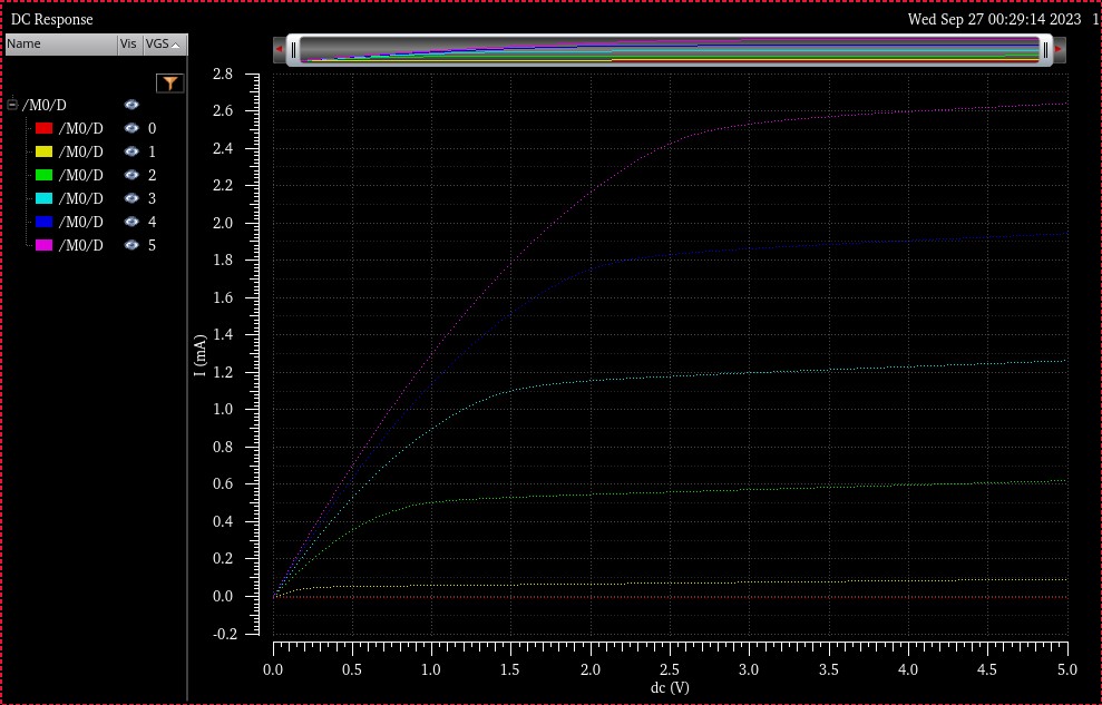
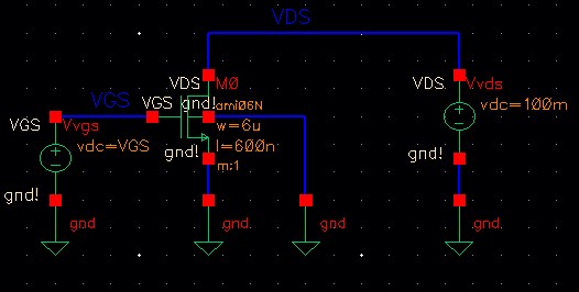
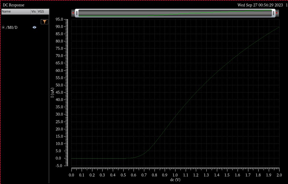
A schematic for simulating ID v. VGS of an NMOS device for VDS = 100 mV
where VGS varies from 0 to 2 V in 1 mV steps. Again use a 6u/600n
width-to-length ratio.
Backup lab by emailing the zip file to my self.
3)
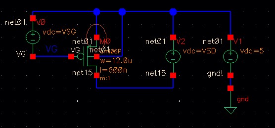
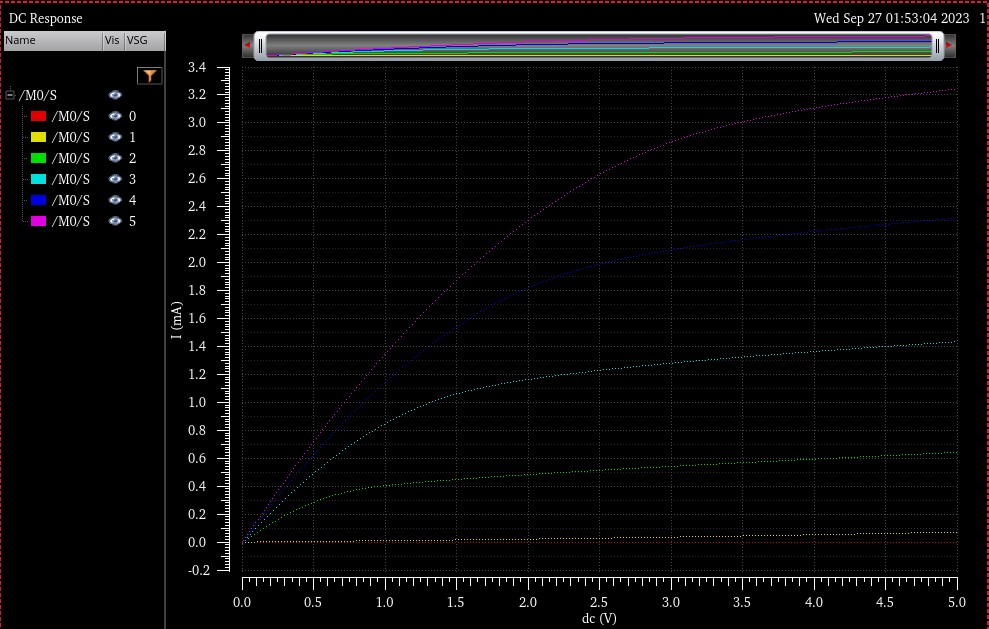
A schematic for simulating ID v. VSD (note VSD not VDS) of a PMOS
device for VSG (not VGS) varying from 0 to 5 V in 1 V steps while VSD
varies from 0 to 5 V in 1 mV steps. Use a 12u/600n width-to-length ratio.
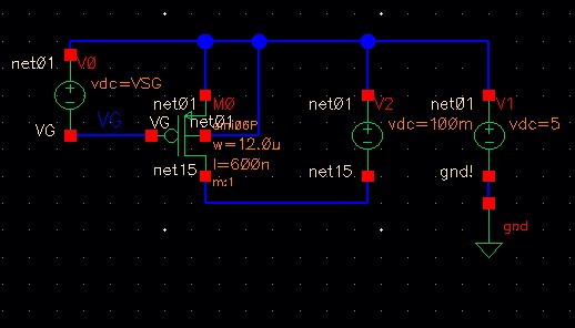
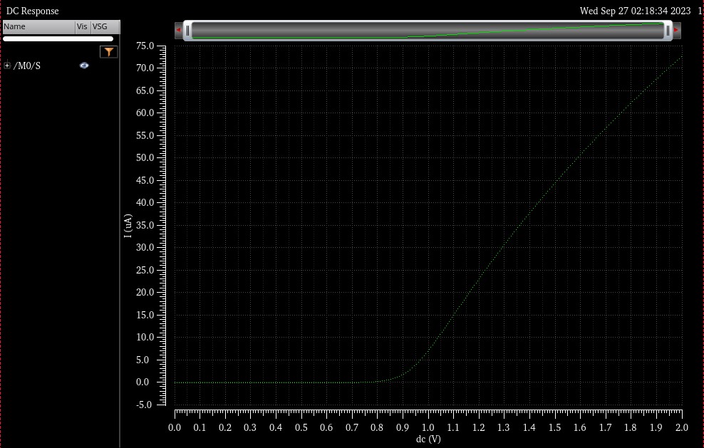
4) A schematic for simulating ID v. VSG of a PMOS device for VSD = 100 mV where VSG varies from 0 to 2 V in 1 mV steps. Again, use a 12u/600n width-to-length ratio.
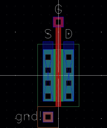
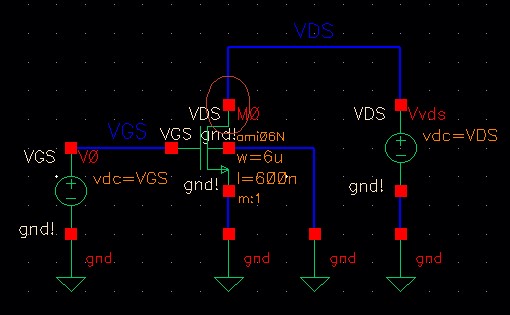
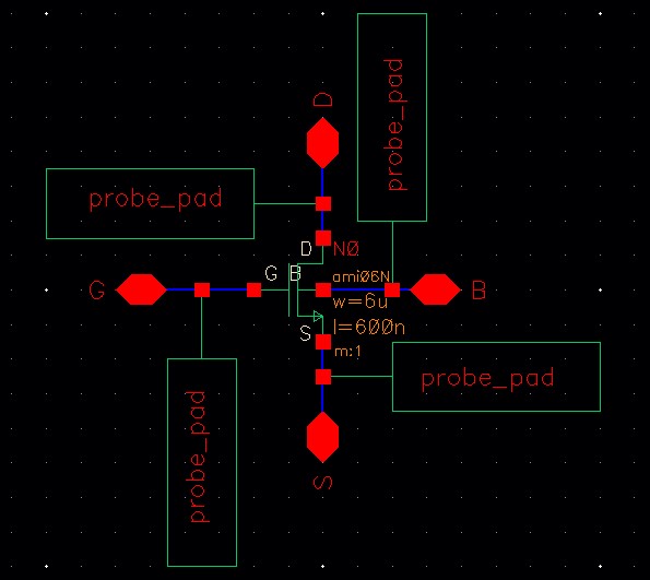
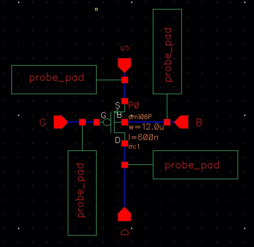
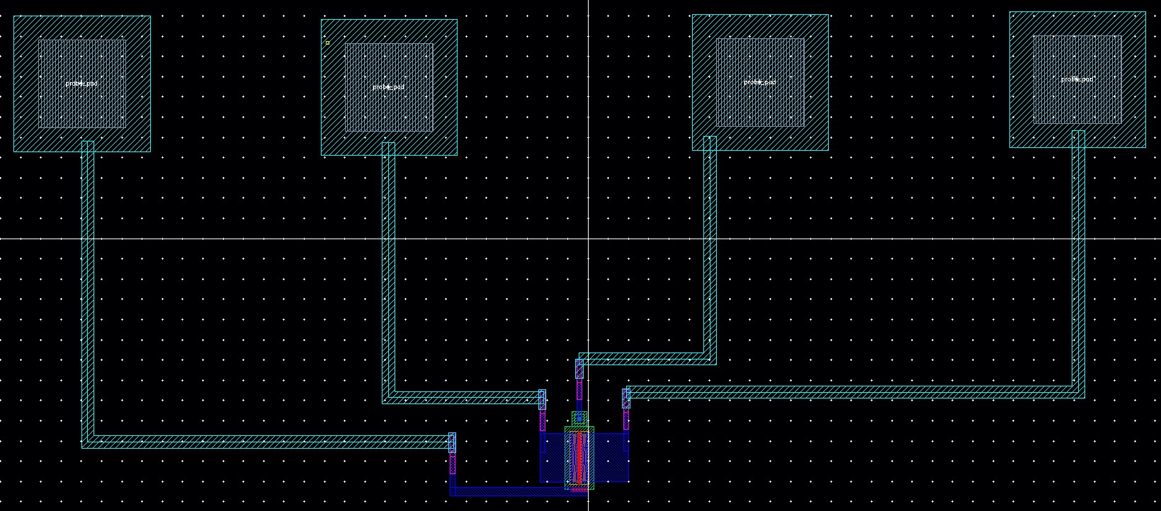
The next part of the lab required me to create a layout and schematic of a NMOS device with all 4 MOSFET terminals to probe pads.
This is the schematic of my NMOS device
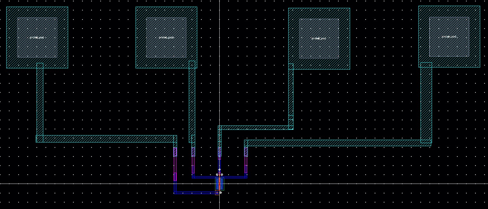
This is the layout of my NMOS device
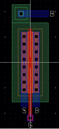
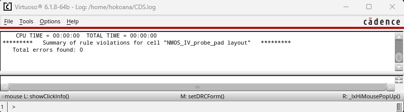
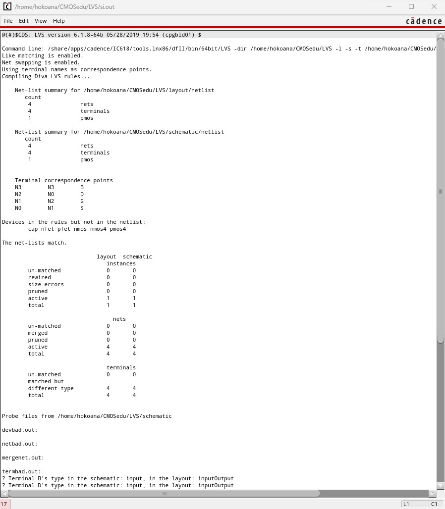
Checking if my layout is DRC and LVS clean

Next I created a schematic and layout for my PMOS device with all 4 MOSFET terminals to probe pads.
This is the schematic of my PMOS device
This is the layout of my PMOS device
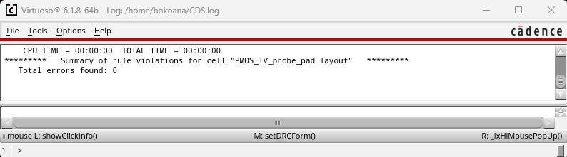
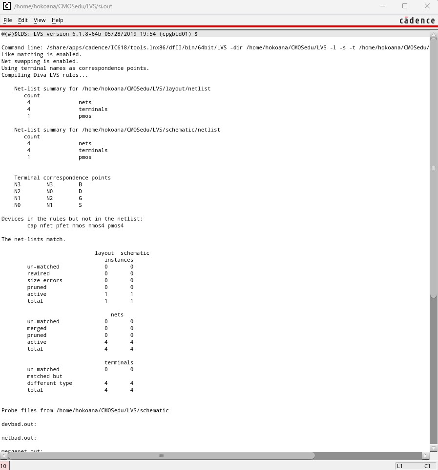
Checking if my layout is DRC and LVS clean

Backing up my work
This completes lab 4.