Lab 3 - ECE 421L
Authored
by Kanoa Hokoana, hokoana@unlv.nevada.edu
September 13, 2023
Lab 3: Designing layout of a 10-bit DAC using 10k n-well resistors
For the prelab I finished up tutorial 1.
The
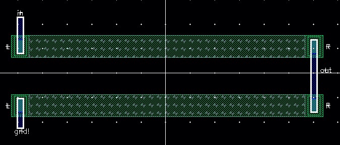
first thing I did is create a layout for a 10k n-well resistor. To get
the dimensions of the n-well resistor I used the equation R = Rs *
(l/w).
R = 10k ohms
Rs = 800 ohms/sq
w = 4.5 um (minimum is 3.6 um)
10k = 800*(l/4.5)
l = 56.25 um
Next I extracted the layout to see the resistance was correct.
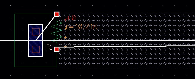
I then created a voltage divider using the 10k n-well resistors.
After this I did a DRC and a LVS check.

This completed tutorial 1 and the prelab.
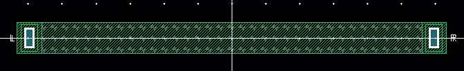
For the main part of this lab I had to create a layout of our DAC using the 10k n-well resistors made in the prelab.
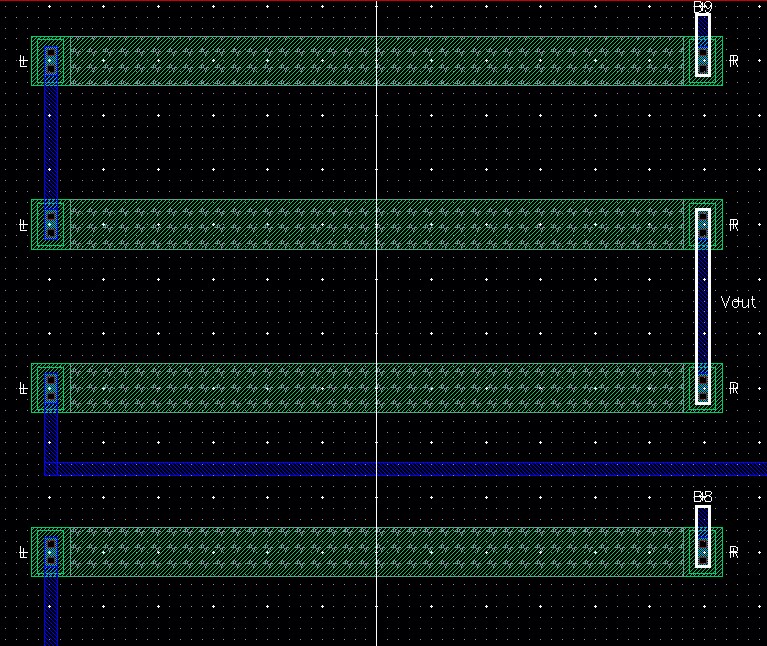
I used this schematic to design my layout of a single bit.
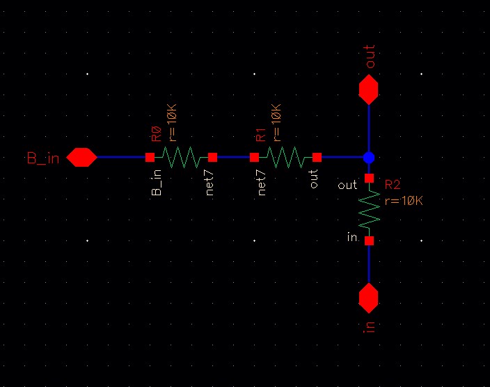
This is the layout of a single bit.
I then used this schematic of my DAC made in lab2 to design the layout of the 10-bit DAC.
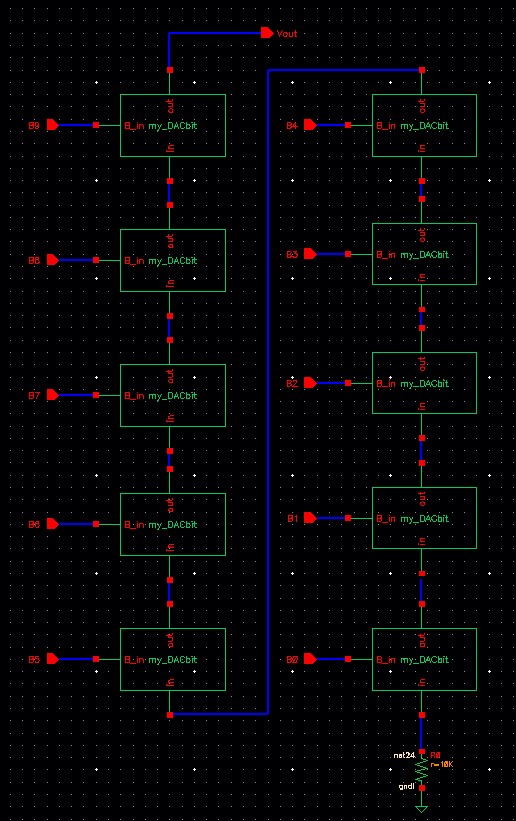
This is the layout I designed.
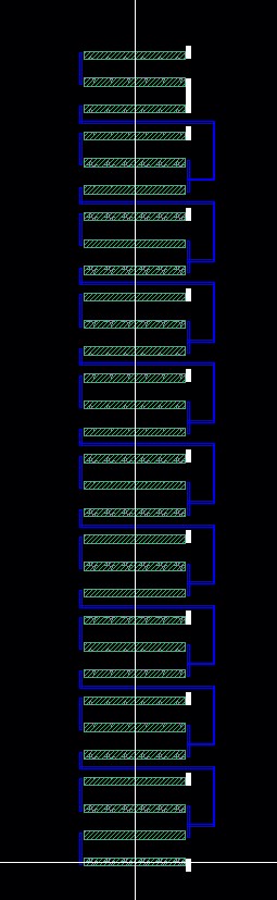
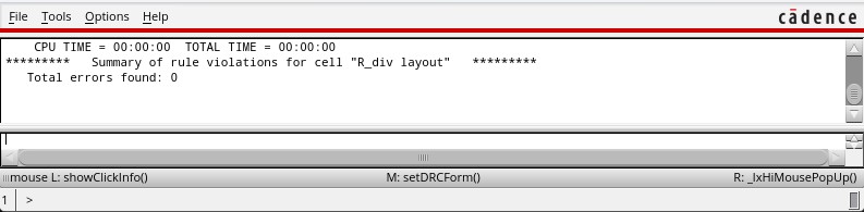
After this I had to do a DRC check.
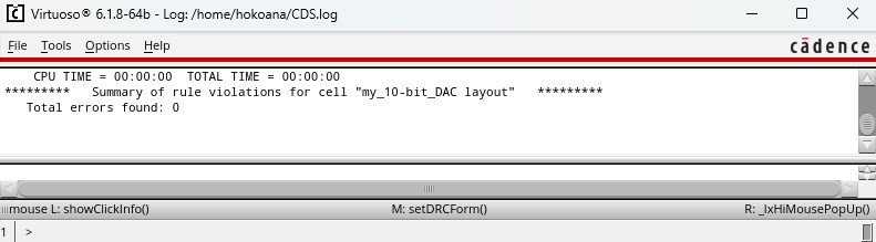
After checking the DRC I then extracted the layout and ran a LVS check.

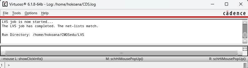
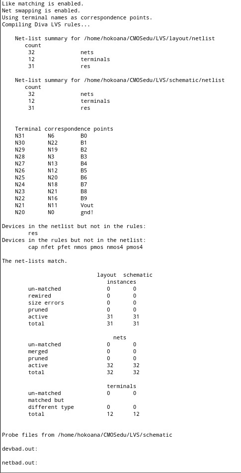
My design passed the LVS check which completed my 10-bit DAC layout and lab3.
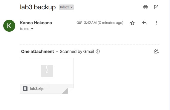
lab3.zip (Final Design Directory)
Backup lab by emailing the zip file to my self.
Return to EE 421L Labs