Lab 2 - ECE 421L
LSB(least significant bit)
The
least significant bit determines the amount of change in voltage is
needed to change the output. This is important because it determines
the accuracy that we are able to measure Vin. To determine
LSB = Vdd/(2^n)
LSB = 5V/(2^10)
LSB = 4.88mV
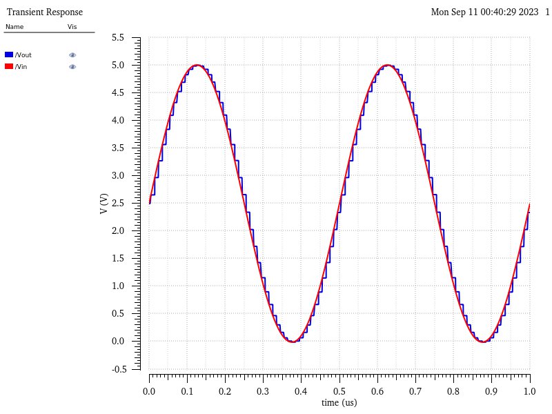
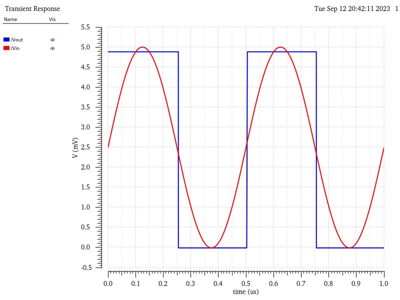
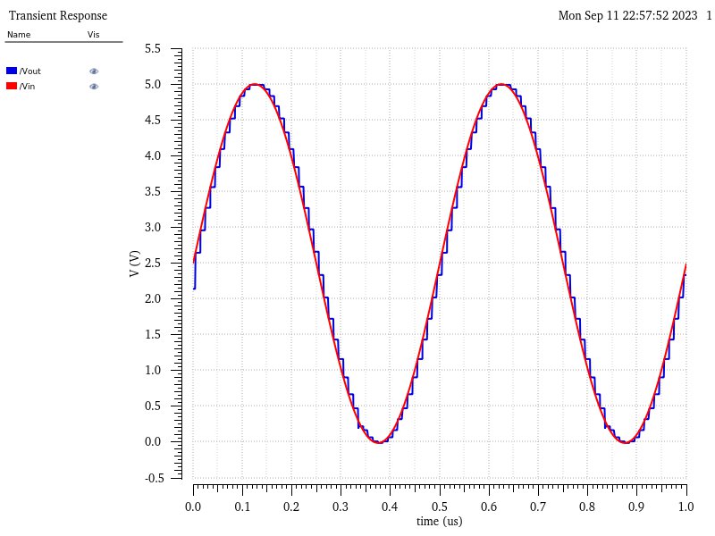
To illustrate this I set the input voltage to 5mV as seen Vout shows 4.88mV and once Vin crosses the threshold of about half of 4.88mV Vout shows the next multiple of 4.88mV which is 9.76mV.
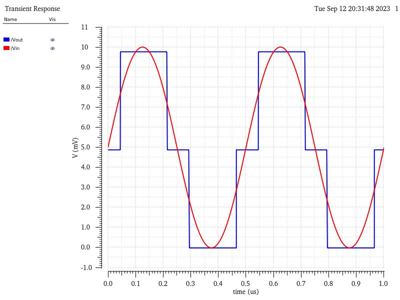
The same can be seen when Vin is changed to 2.5mV when below 2.5mV Vout measures 0V because that is the closest multiple of 4.88mV. Meaning it can only measure and output the binary code that represents a multiple of 4.88mV
To determine the total output resistance we can better understand by looking at the design of an DAC.
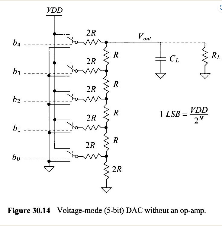
From this we are able to see that the resistors are in parallel and series. By reiterating this instance we will find that the final output resistance is 10k.
2R||2R = R
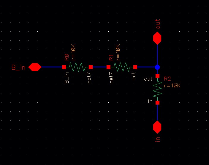
To first start designing my 10-bit DAC I made a schematic of single bit within a DAC that functions like a voltage divider.
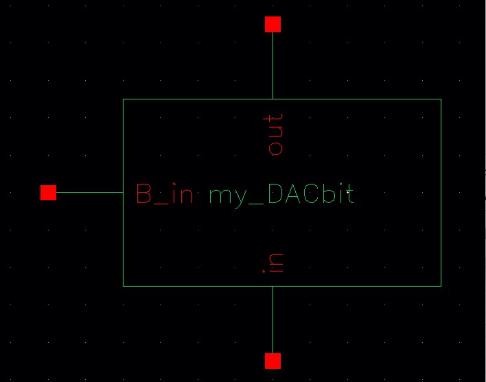
I then created a symbol so that I could more easily incorporate this into the bigger schematic.
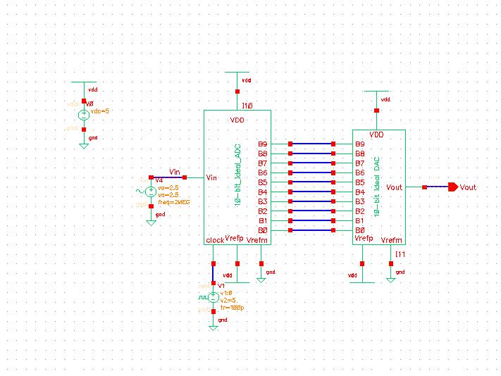
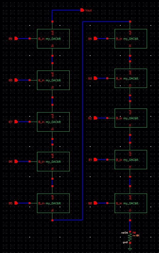
From here I created a new schematic and used the created symbol to get a 10-bit DAC. I then added the pins B[9:0] to the input pins of each bit and added a 10k resistor and gnd to the bottom of the DAC to achieve the example design of a 5-bit DAC shown in the prelab.
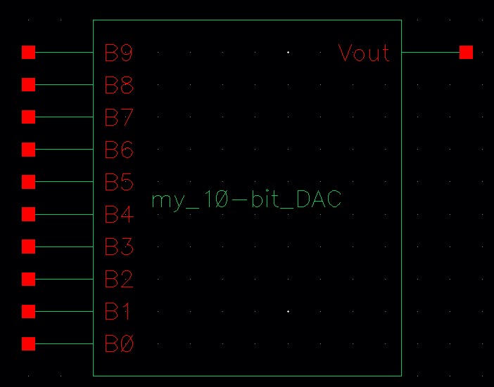
From here I created another symbol that would be easier to incorporate into the bigger schematic.
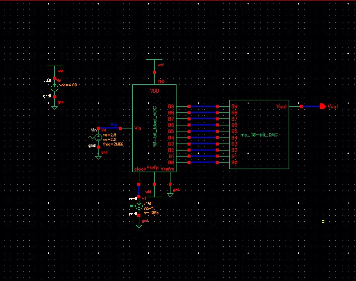
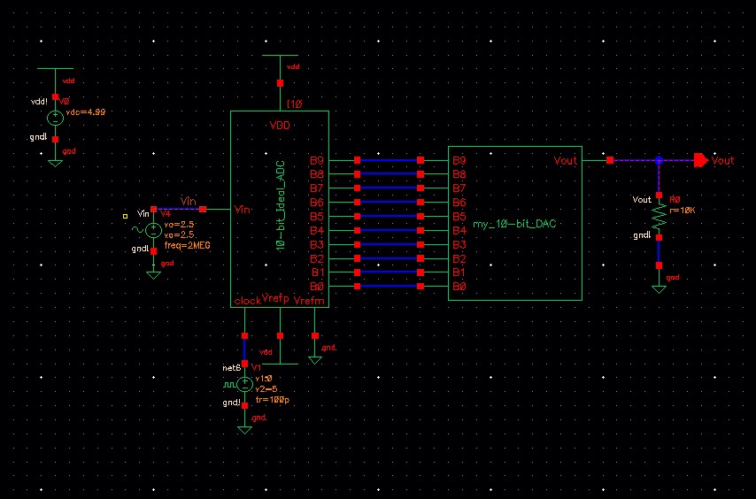
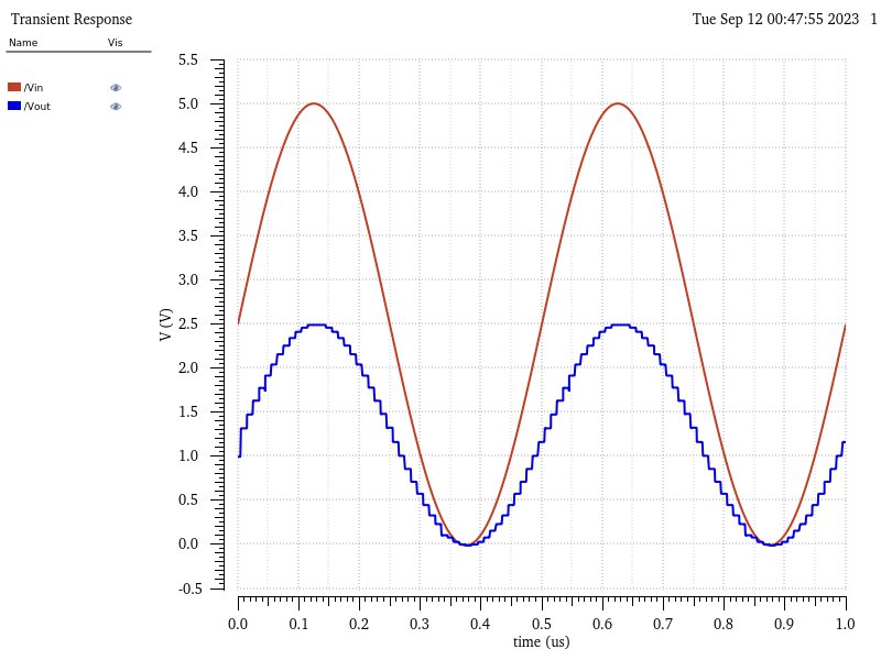
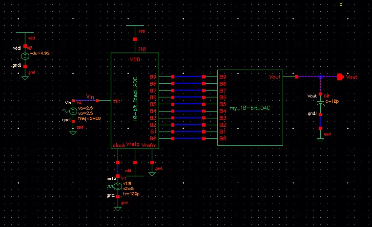
With this symbol created I was able to connect my DAC that I designed to the ideal ADC for simulation. The simulation results closely match the ideal simulated DAC. To achieve this I needed to force the simulation to converge as well as change Vdd to 4.99V.
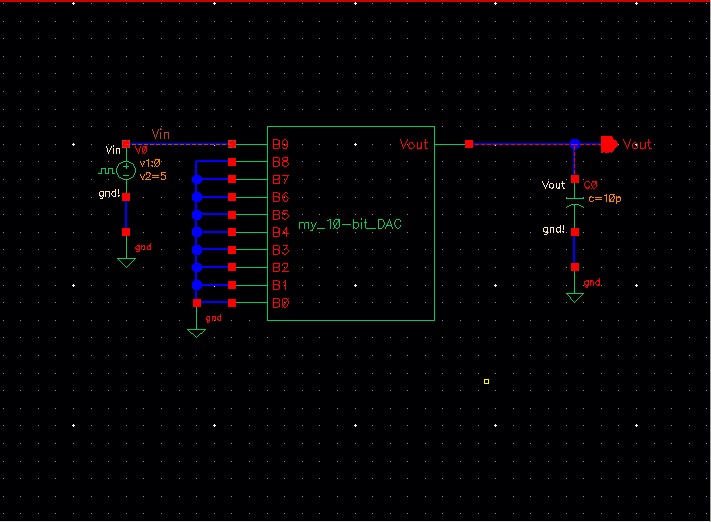
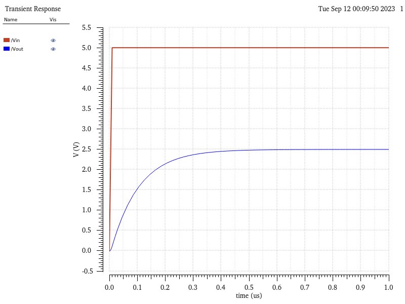
Next I wanted to find the delay the DAC has driving a 10 pF load. To do this I grounded all bits except for B9 and created a pulse source that went from 0V to 5V. To calculate the delay we use the equation 0.7RC.
0.7(10k)(10p) = 70ns
To verify that my design was working correctly I ran simulations with my DAC driving a load. First was a 10kohm resistor this caused the output to be halved as it became a voltage divider.
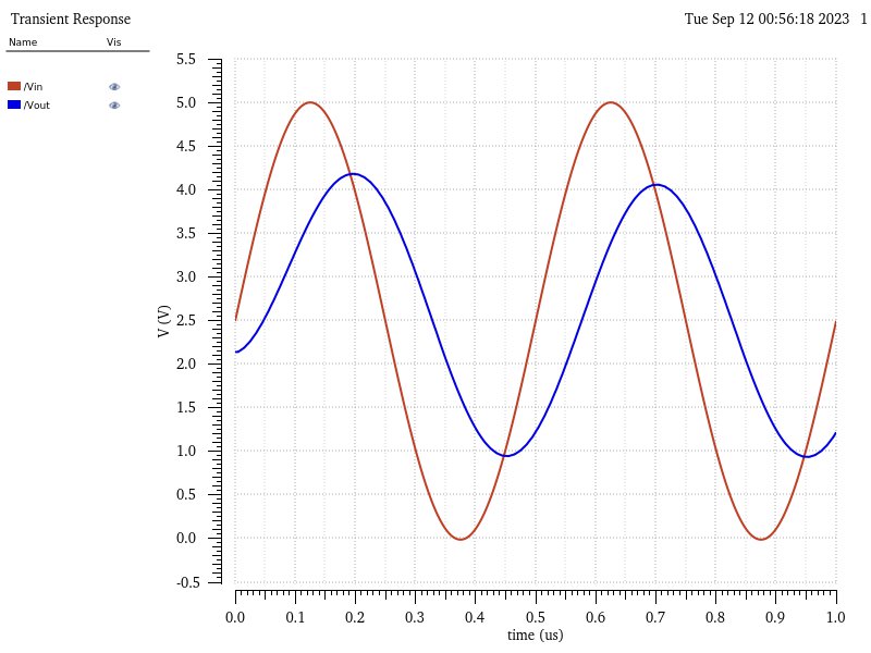
I then simulated my DAC driving a 10pF capacitor. This showed a delay in Vout and also smoothed and decreased the output.
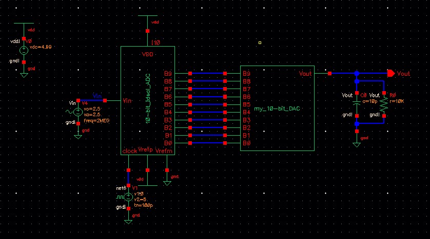
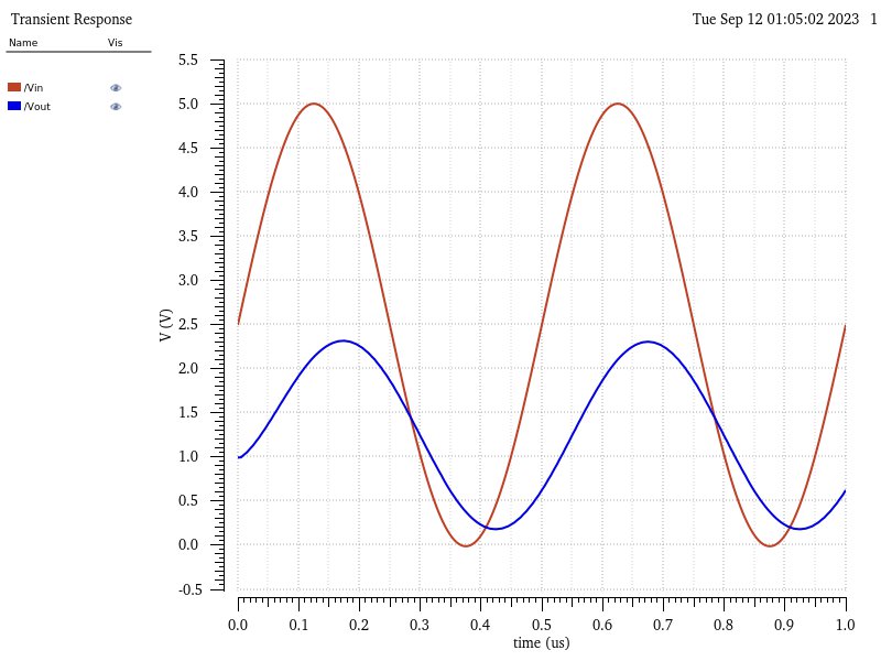
The last load was both the resistor and capacitor in parallel. This further decreased the output and also smoothed and delayed Vout.
In a real circuit the switches seen in Figure 30.14 are implented with MOSFETs. If the resistance of those switches isn't small compared to R the output resistance would be much higher and would lower Vout. This is due to the switches being in series with the DAC resulting in a higher resistance.
As always at the end of this lab I backed up my work by compiling everything into a .zip file and emailing it to myself.