Lab 8 - ECE 421L
~~~~~~~~~~~~~~~~~~~~~~~~~~~~~~~~~~~~~~
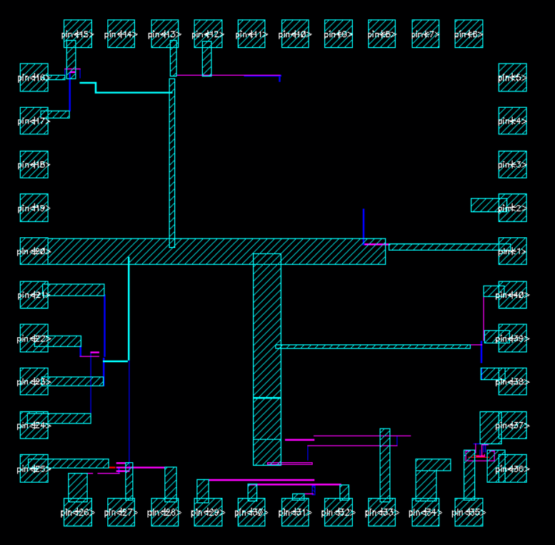
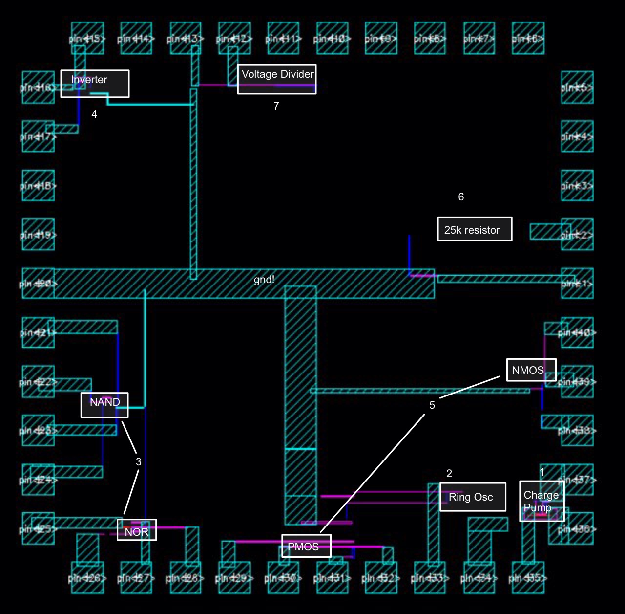
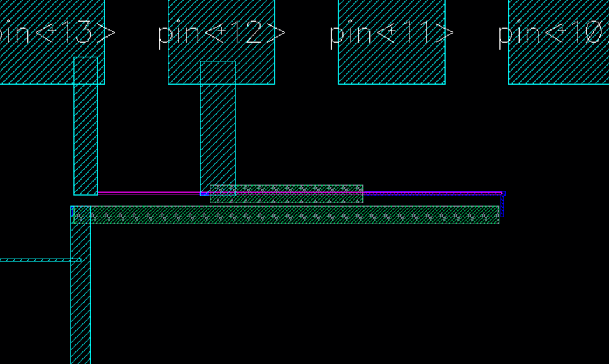
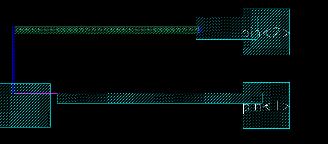
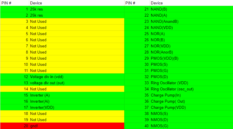
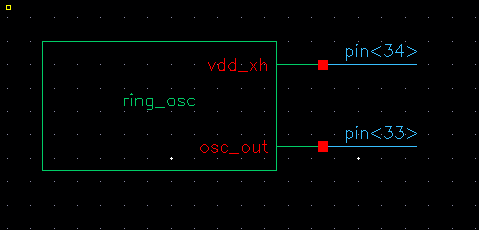
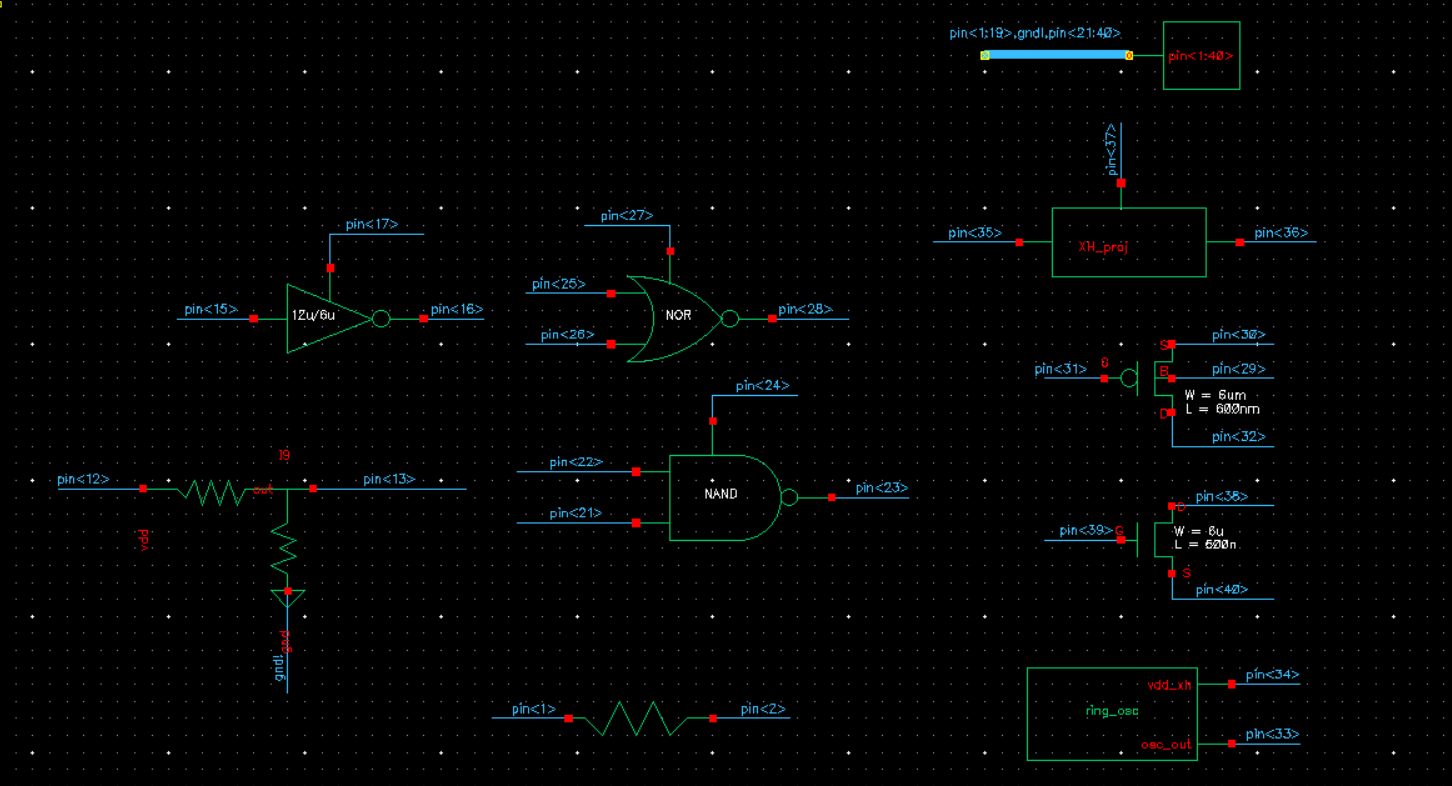
Full Pin Callouts
Testing:
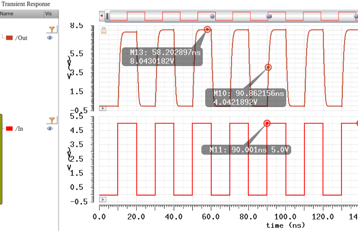
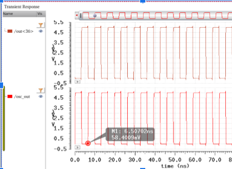
Pin 34 for vdd and pin 33 for oscillation output.
Testing:
Simply supply a voltage supply to pin 34, and watch the oscillations from pin 33
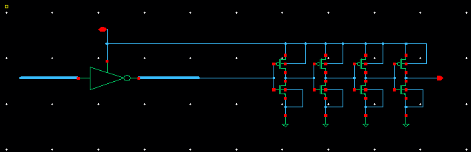
Simulation:
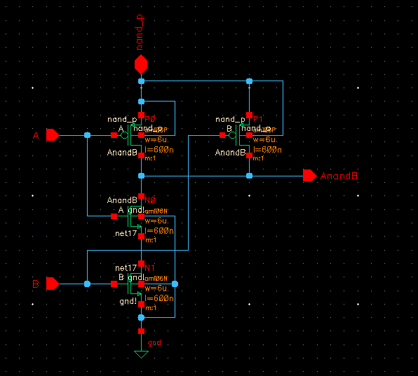
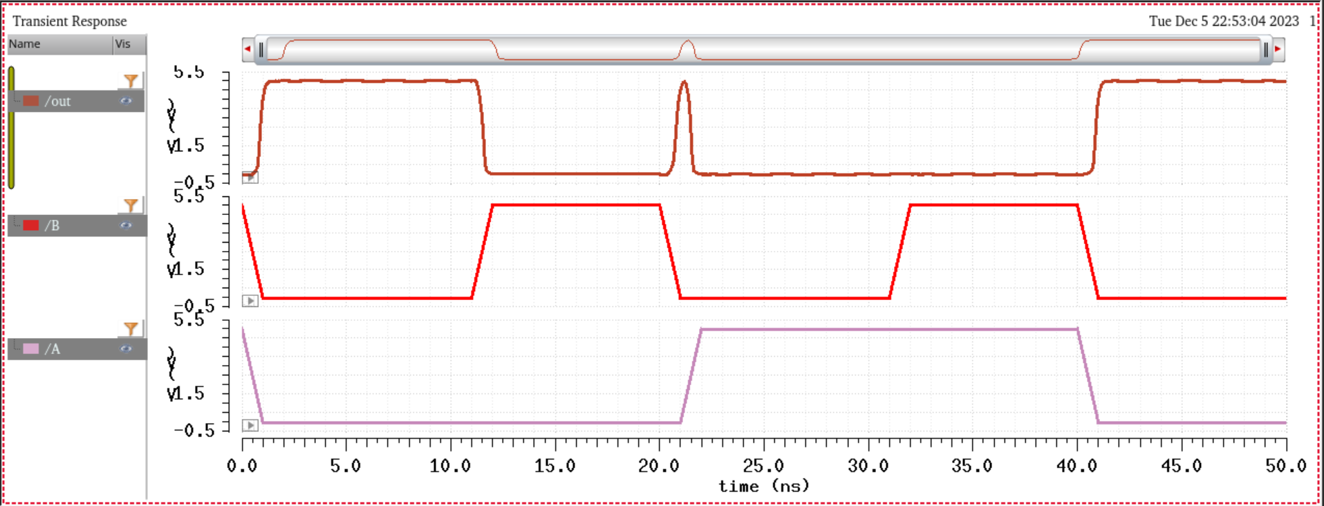
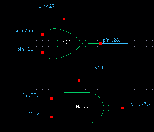
3. NAND and NOR gates
Schematics:
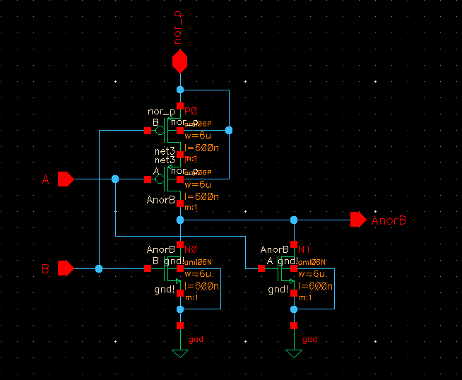 | 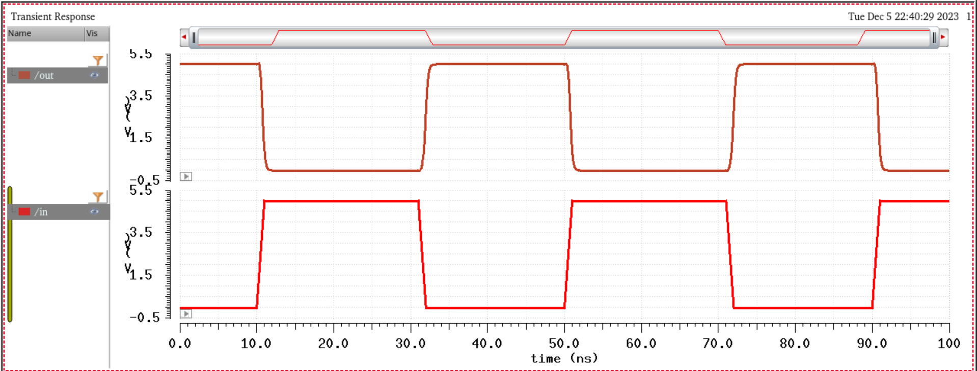 Note that VDD was connected to one of the input pins of the NAND gate so A is always 1 (not shown in this sim). In is the B pin. |
 |  |
Testing:
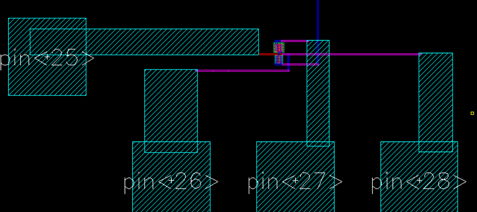
To test NOR, simply provide high or low inputs to either 25 or 26, and constant supply to pin 27, and record the output, 28.
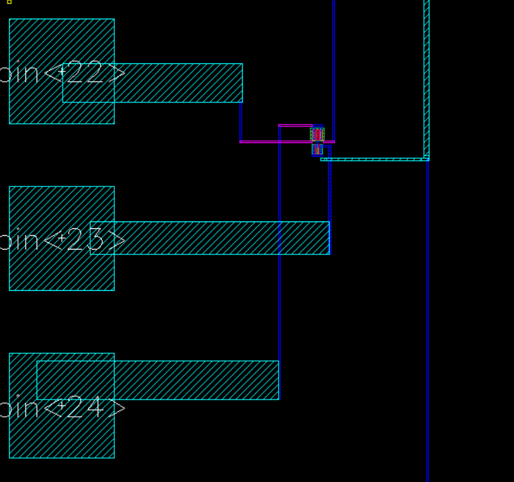
To test NAND, provide high or low inputs to 22 or 21, a constant supply to pin 24, and record output 23.
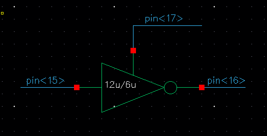
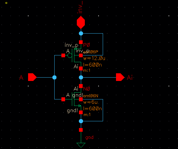
4. Inverter with PMOS/NMOS 12u/0.6u
Schematic:
Testing:
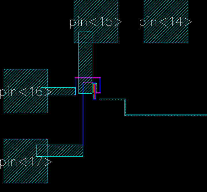
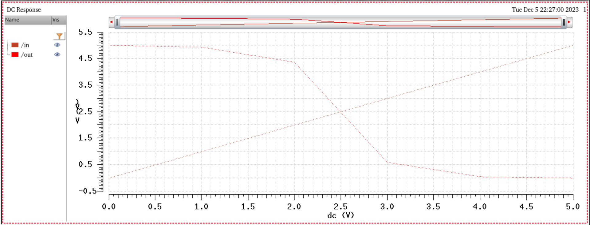
To test, simply apply an input to pin 15, watch the inverted output at pin 16 and provide a constant supply to pin 17
Simulation:
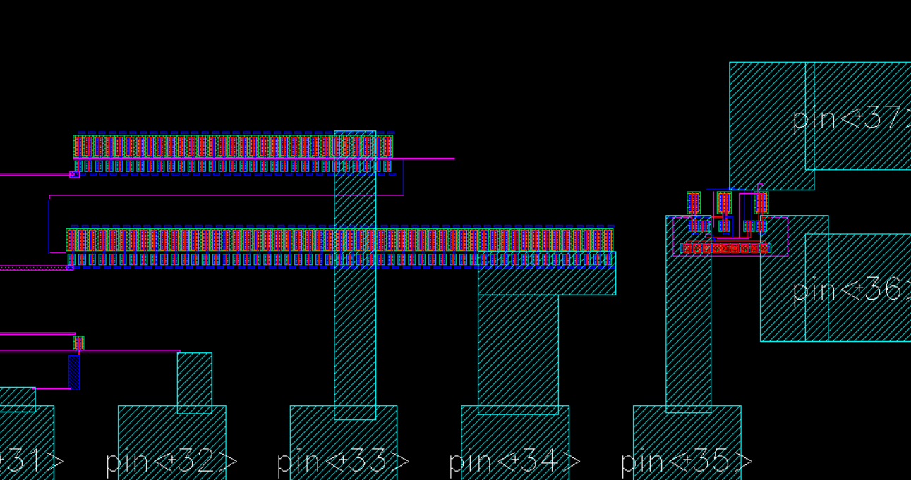
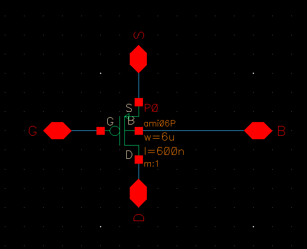
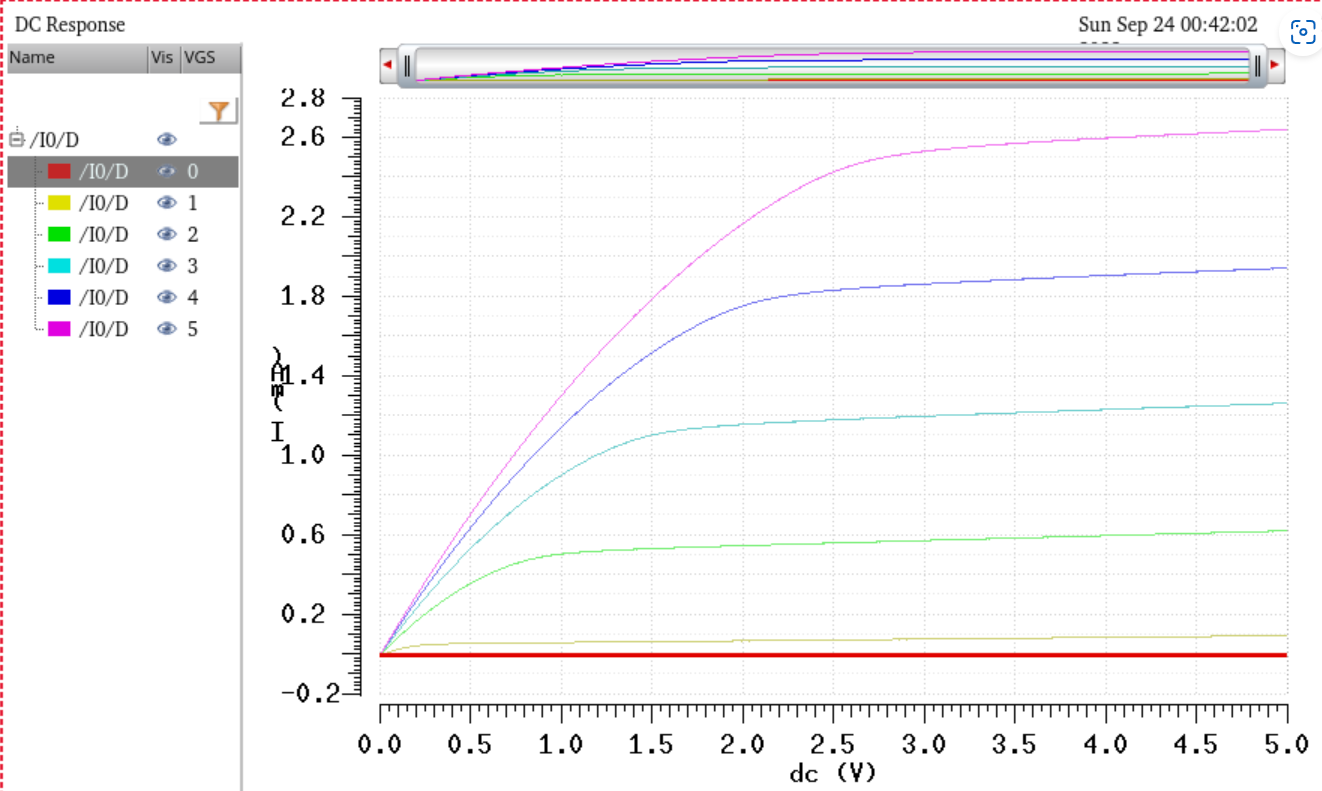
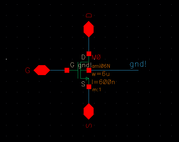
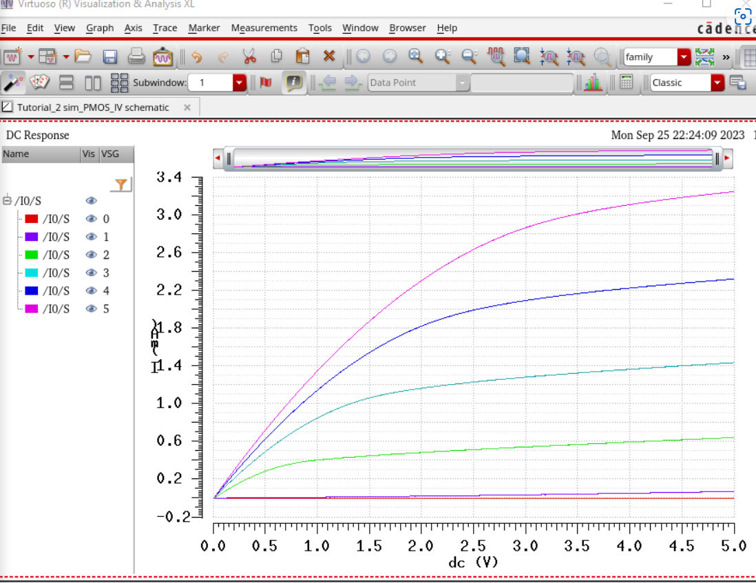
5. PMOS/NMOS transistors
Schematics:
Old simulations for IV curves of exact same NMOS/PMOS and corresponding symbol provided.
 |  |
 |  |
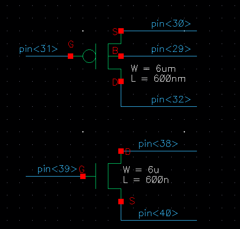
To test,
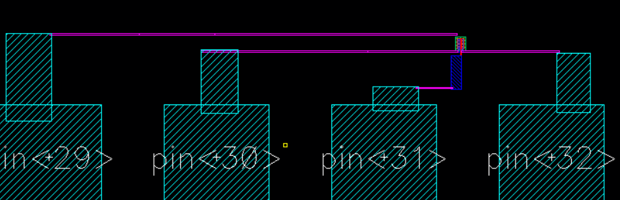
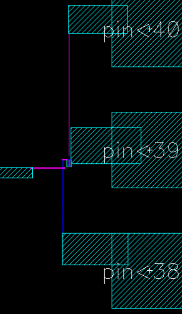
Simply provide any input or measure any output to 29,30,31, and 32 for PMOS
Provide any input or measure any behavior/output to 38,39,40 for NMOS
To observe appropriate outputs, one must remember transistor operating regions.
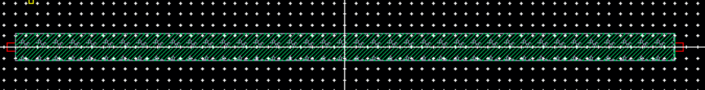
6. 25k resistor using N well
N-well layout 300u * 12u
Pin 1 is left, Pin 2 is right
To test: Simply apply a voltage to either pin 1 or 2, and measure the voltage drop, or current, or resistance across) the other pin not that wasn't previously usd
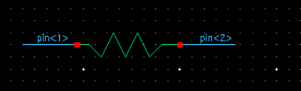
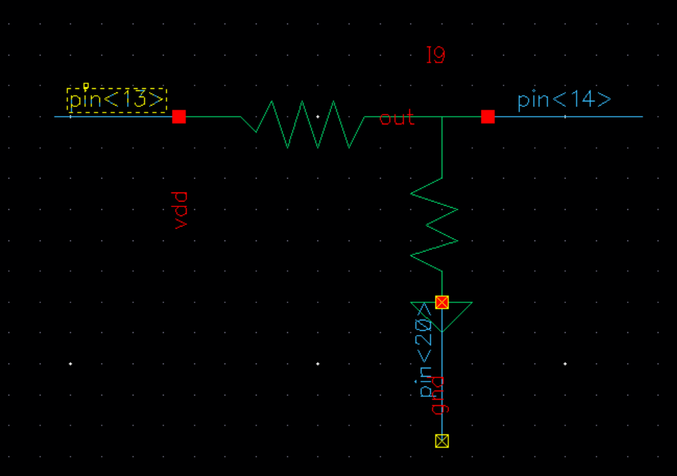
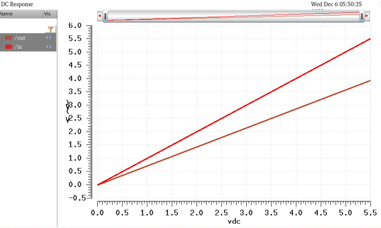
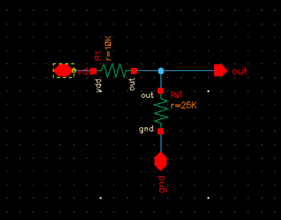
7. Voltage divider using 25k and 10k resistors.
the voltage divider drops the voltage by a ratio of 0.71
Pin 13 is the input voltage. Pin 14 is the output voltage. Pin 20 is the grounded output of the second resistor.
Testing: Simply provide an input voltage to 13 and observe output from pin 14.
Simmed with DC Sweep
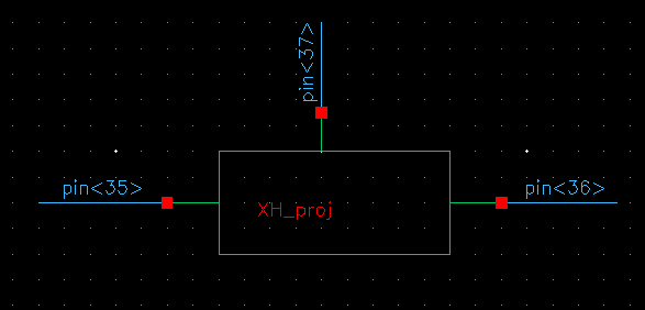
Top Level Cell Chip Schematic + Cell View:
Schematic
Layout