
Lab 7 - ECE 421L
Then we label the wire connecting the final and first inverter.
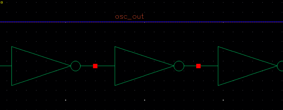
Now we can simulate. If we do not set an initial condition to the circuit. Then the simualtion would flatline at 2.5V
So we an inital condition of 0V is set to the osc_out wire.
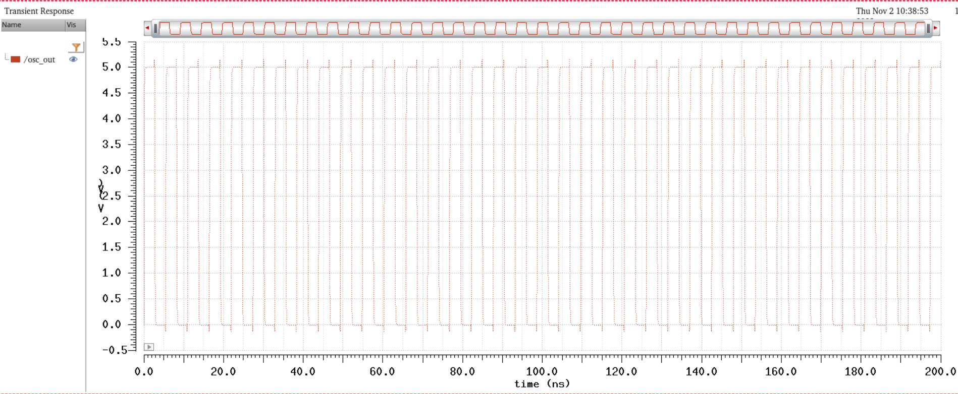
And after simulating with that inital condition, then these are the results.
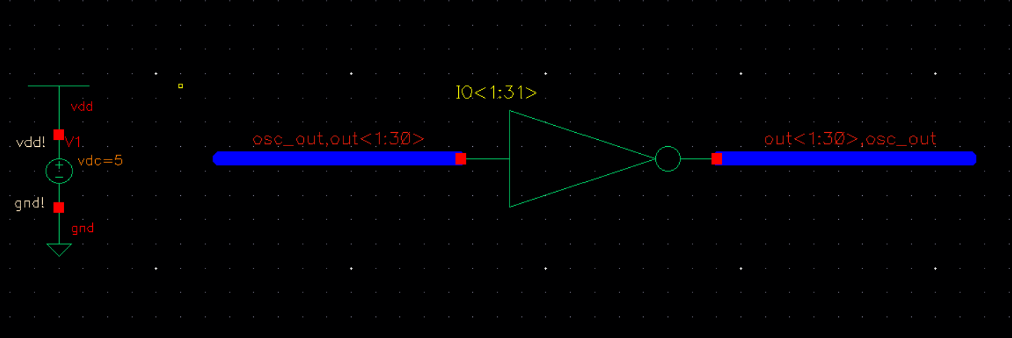
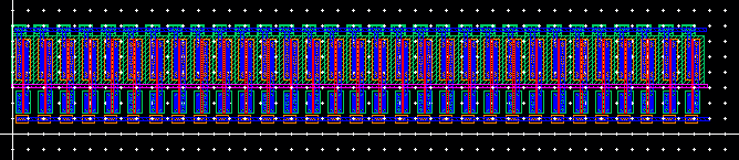
The schematic used is fine however it might be messy to look at, a cleaner version can be made. Using wide wire (which makes an array), then we can reduce our schematic to using a single inverter.
This new schematic is the exact same as the one above.
I<31> represents the final inverter and its output is osc_out (out<31>), the input out<30> is the output of I<30>, which is the previous inverter
The others are self explanatory with I0<1> being for inverter 1 and it's input/outputs being osc_out and out<1> respectively. And continues on with each subsequent inverter.
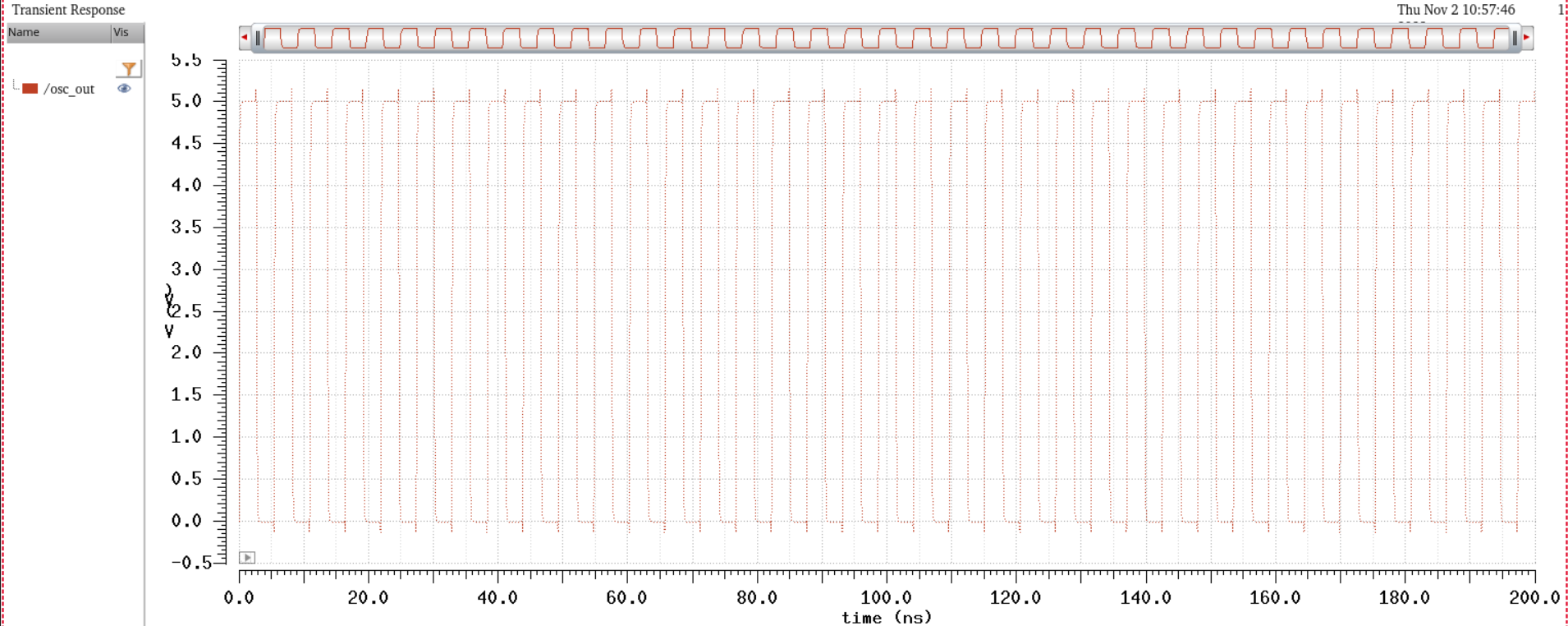
Now we sim this new schematic. As expected the simulations are the exact same between the larger schematic and the cleaner array schematic.
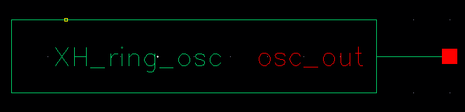
Below is my ring oscillator symbol.
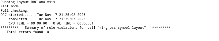
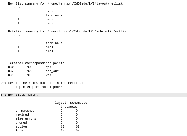
Finally here is DRC check, and LVS check, both passing.
Labwork
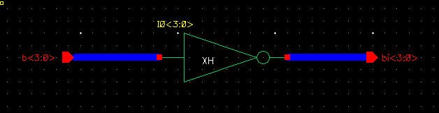
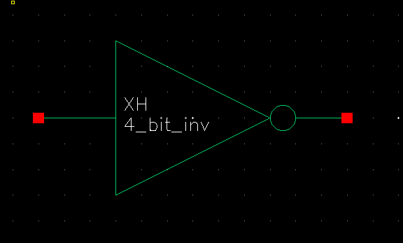
We first start off with building the 4 bit inverter and it's corresponding symbol.
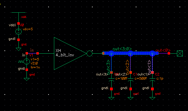
Then we use the 4 bit inv to drive 3 different capacitance loads: 100fF, 500fF, and 1pF, and also no load.
And these are the results:
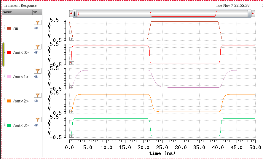
Clearly it can be seen that smaller capacitances reduce the delay and rise/fall times.
The bigger capacitor, out<1>, has the largest delay, and also the largest rise/fall time.
The smallest capacitor, out<3>, has almost the same delay and rise/fall times as if there was no capacitor.
Next we are to simulate a 2 to 1 MUX/DEMUX.
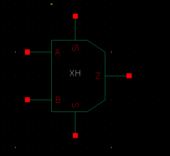
First we design the schematic, as well as it's corresponding symbol.
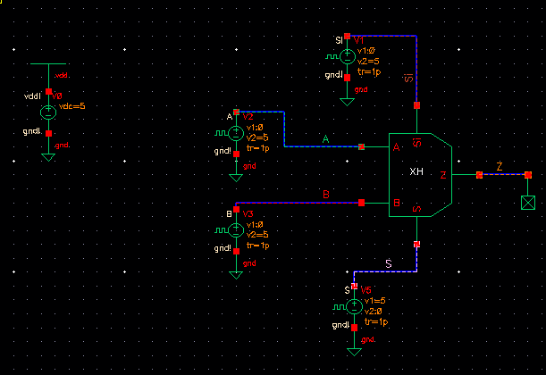
MUX sim schematic:
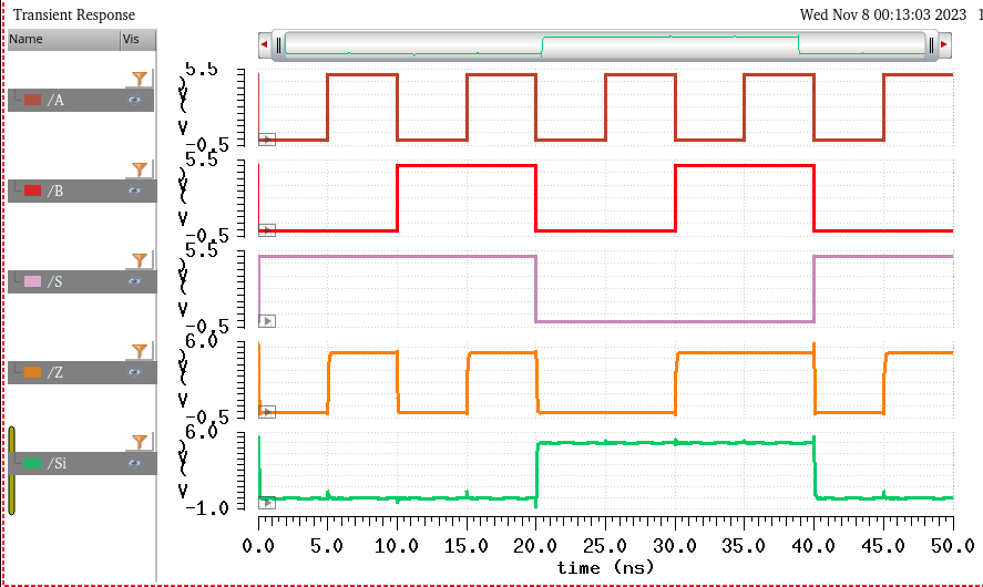
Mux sim results:
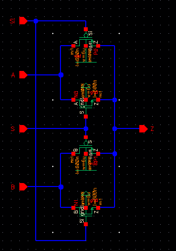
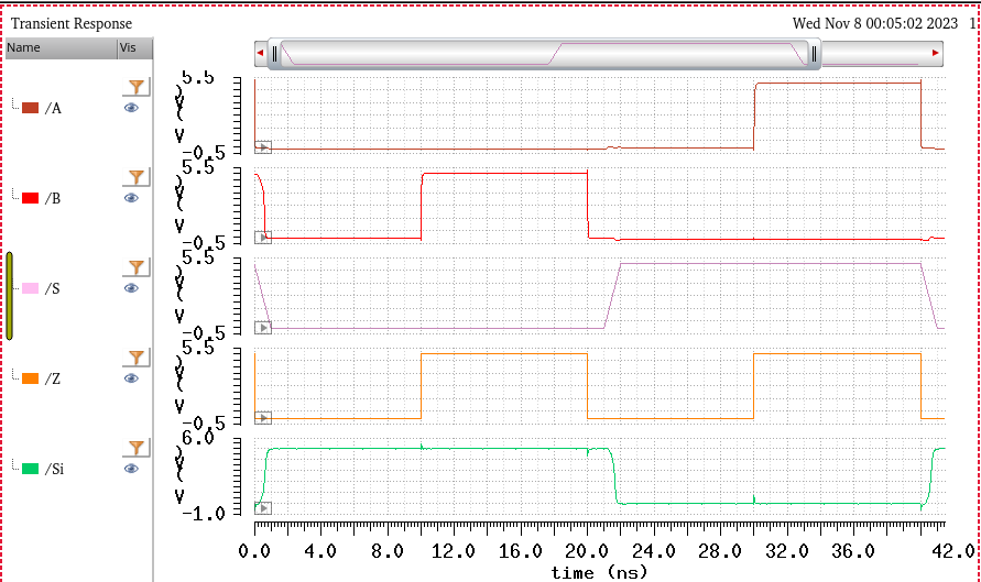
DEMUX sim schematic:
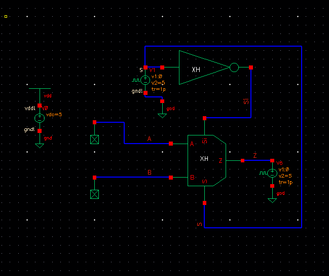
DEMUX sim results:
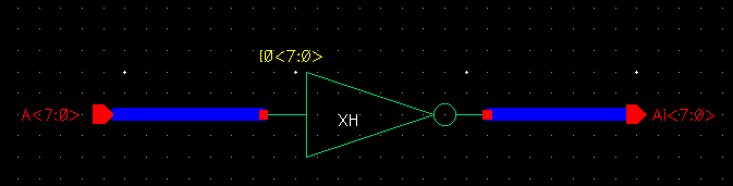
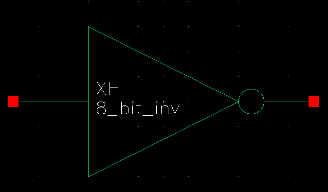
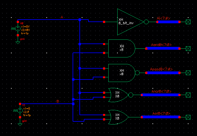
Next we will make the 8 bit inverter and its corresponding symbol.
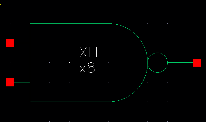
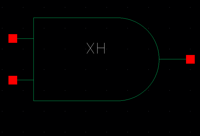
8 bit NAND, symbol and schematic, using NAND from previous lab.
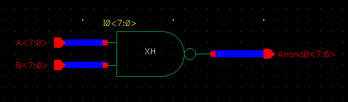
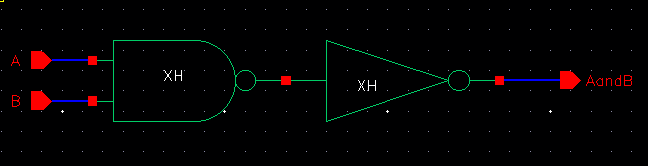
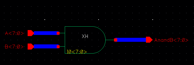
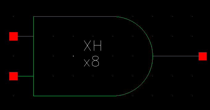
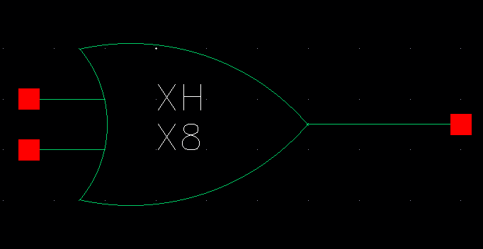
8 bit AND, simply adding an inverter to the NAND.
1 bit first:
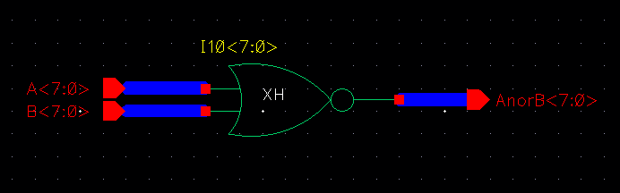
8 bit NOR:
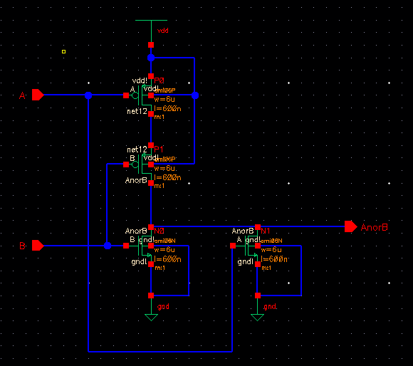
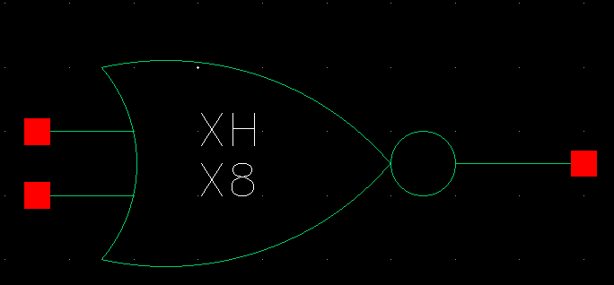
The 1 bit NOR first.
Schematic:
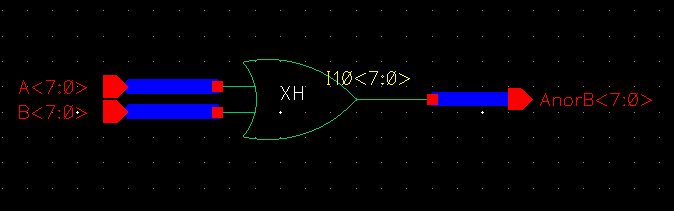
Then 8 bit schematic using NOR symbol, and the corresponding 8 bit NOR
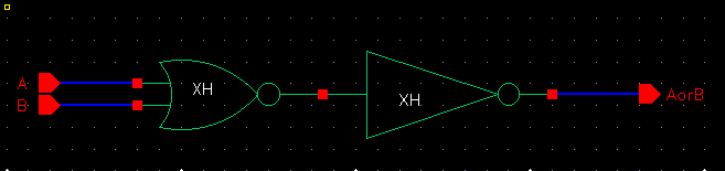
8 bit OR:
Similar to AND gate, an inverter is simply added to the NOR gate to create the OR gate
1 bit symbol: 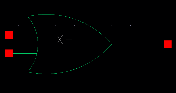
And the 8 bit schematic/symbol:
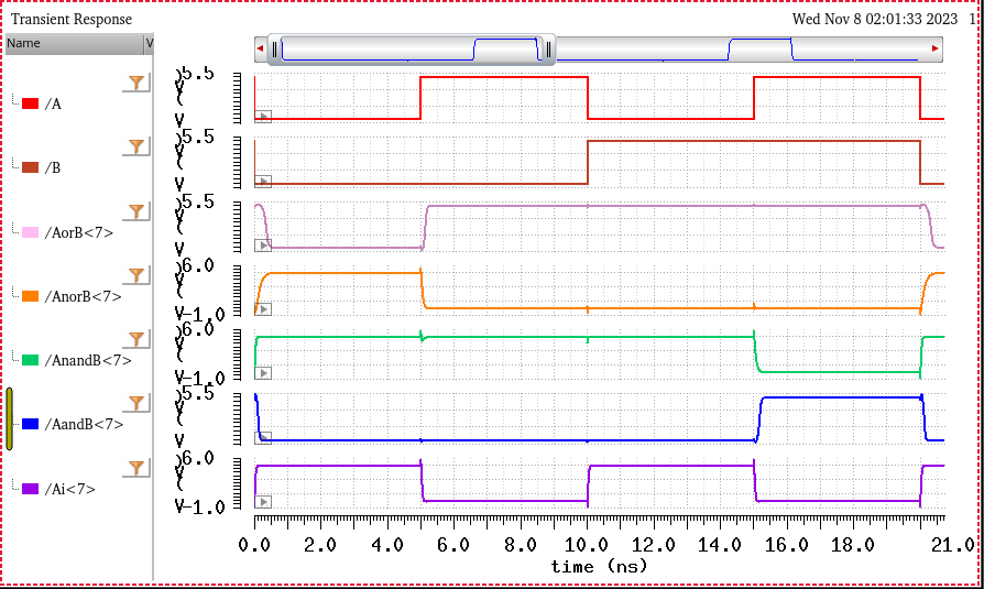
Finally here are the simulations of all 5 gates:
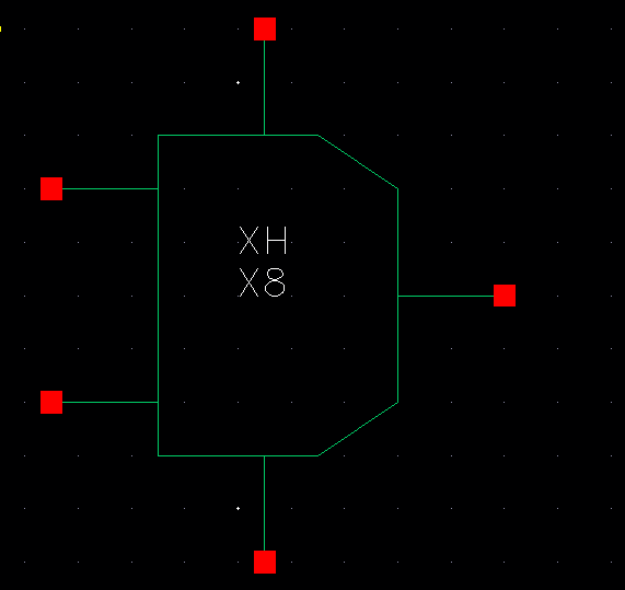
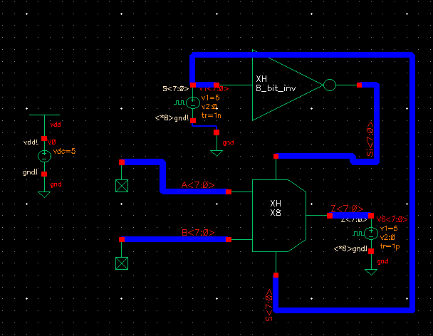
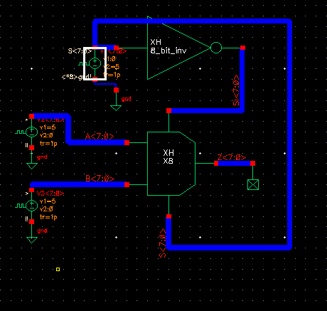
Next we design the 8 bit 2-to-1 DEMUX/MUX.
We simply modify the DEMUX/MUX already built.
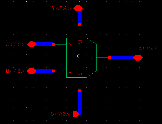
And its corresponding symbol:
DEMUX schematic and sims:
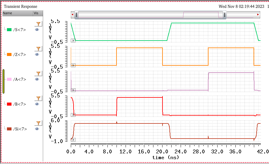
Again, the sims behave as expected, similar to the 1 bit MUX.
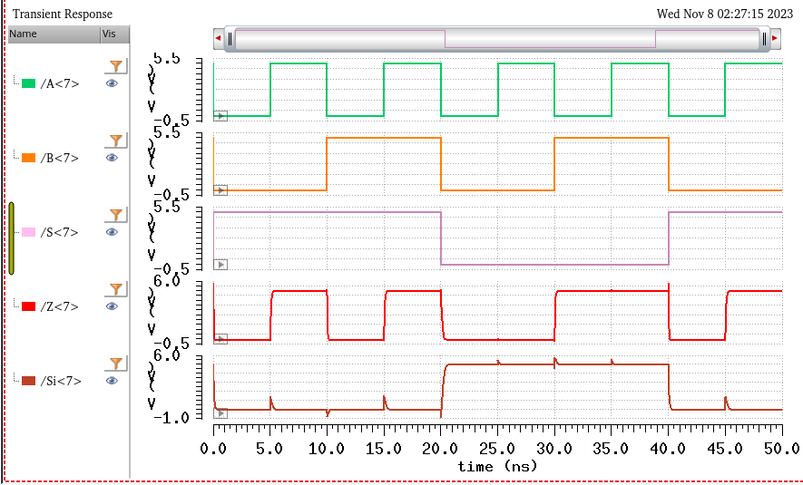
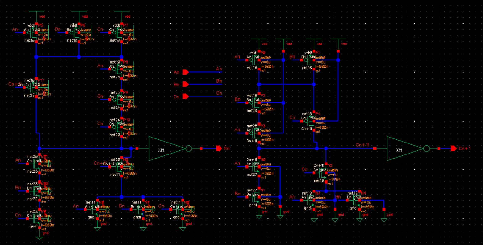
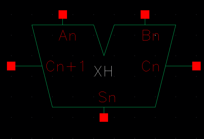
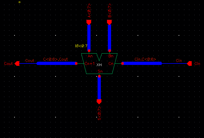
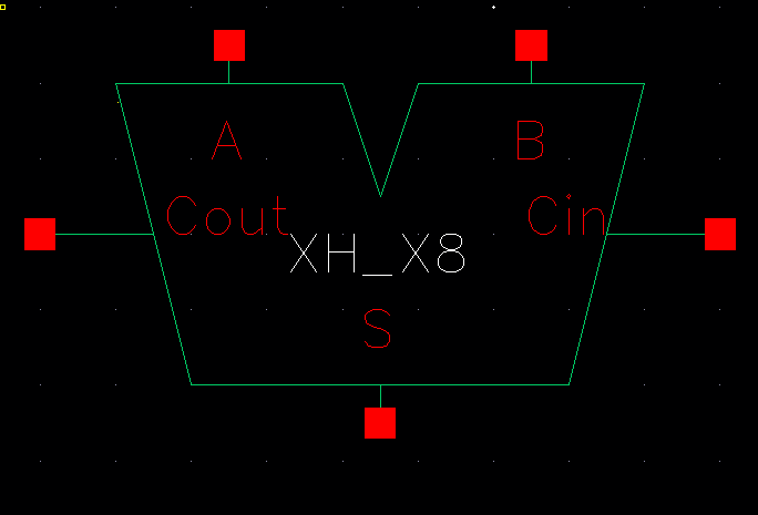
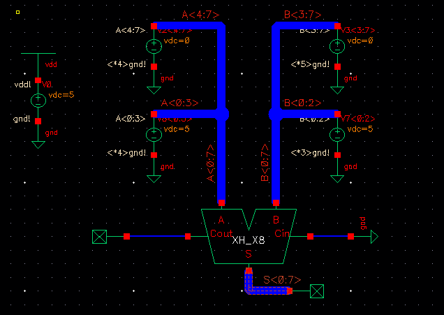
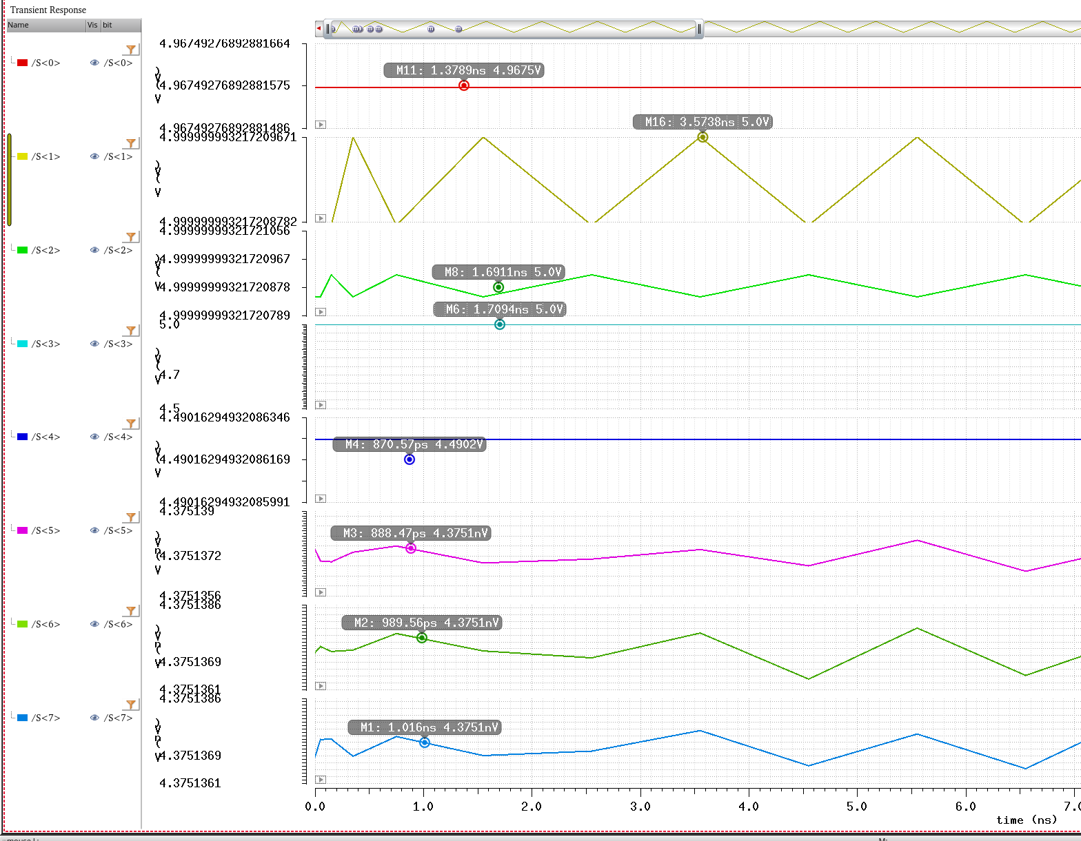
8 bit Adder:
First we design a singular adder with design following fig 12.20, using 6u/0.6u NMOS/PMOS devices.
Return to Xavier's Labs
Return to EE421 Labs