Lab 6 - ECE 421L
10/25/23
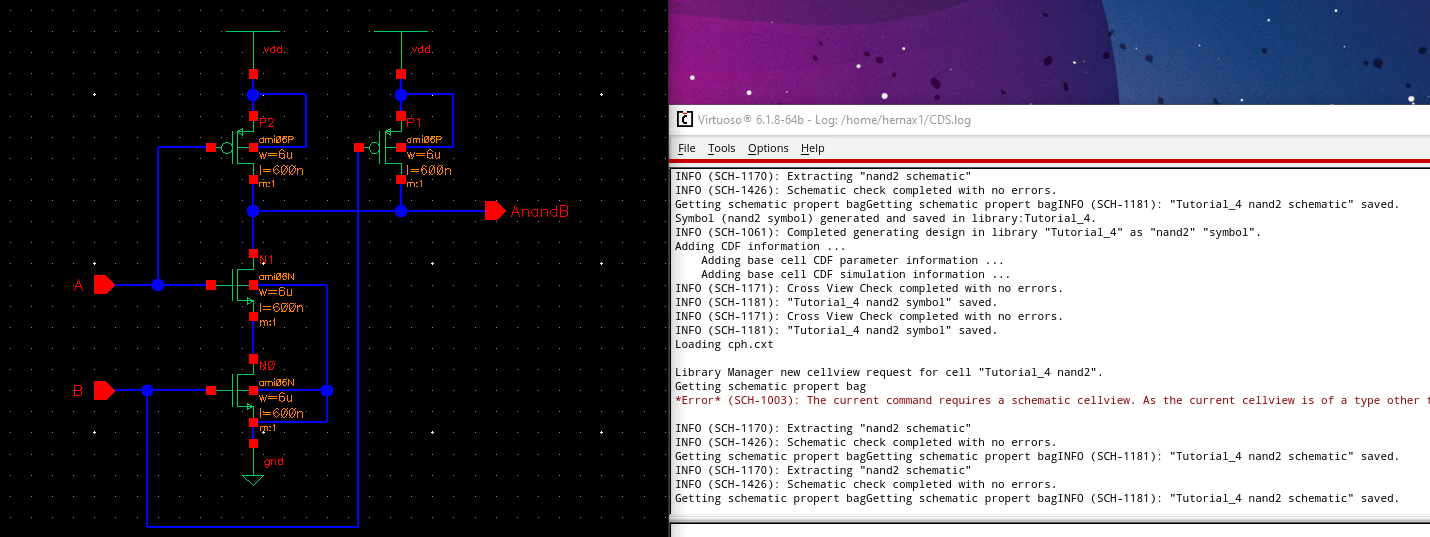
To begin we create the NAND schematic.
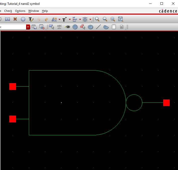
Then we create the NAND symbol
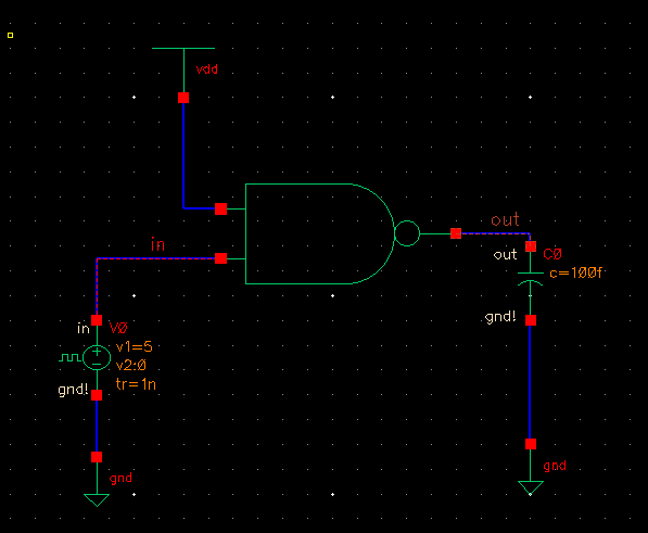
Now we can simulate using our NAND symbol, we sim this circuit
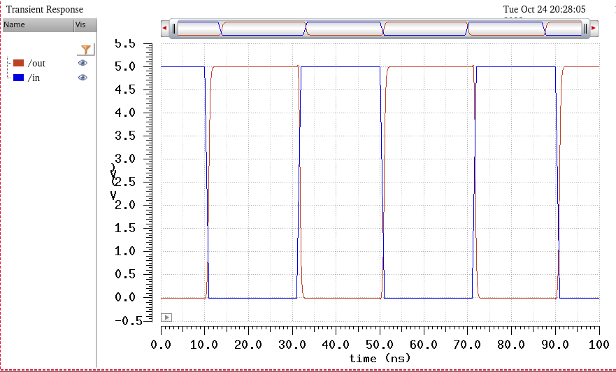
And then we get these results
And extracted:
NAND gate
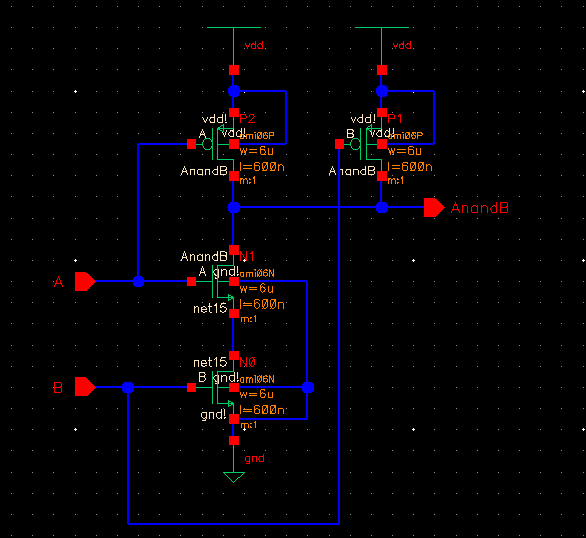
NAND gate schematic and the corresponding symbol: 6u/0.6u
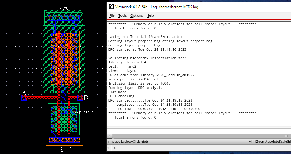
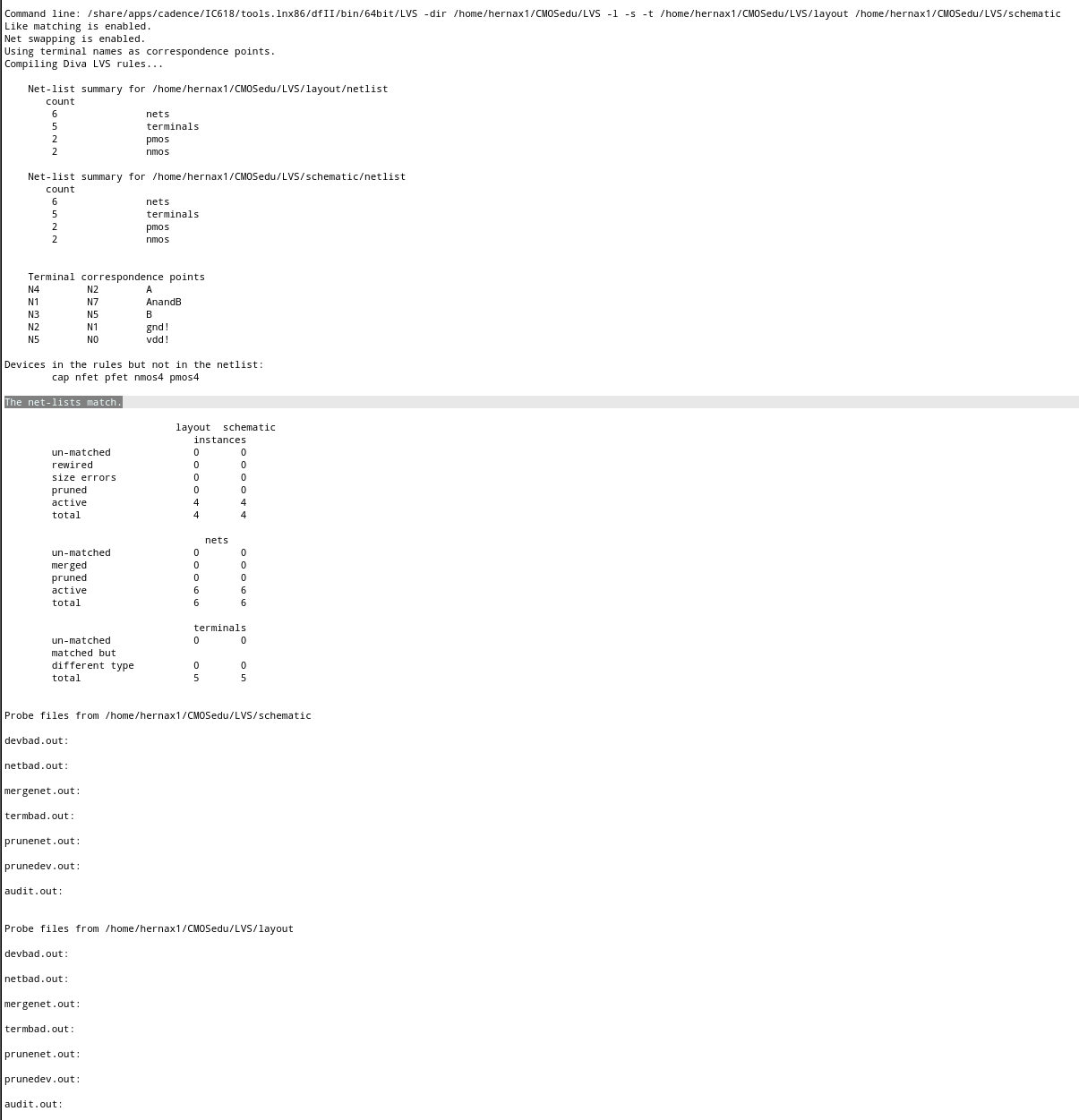
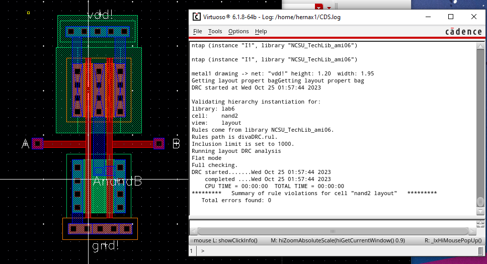
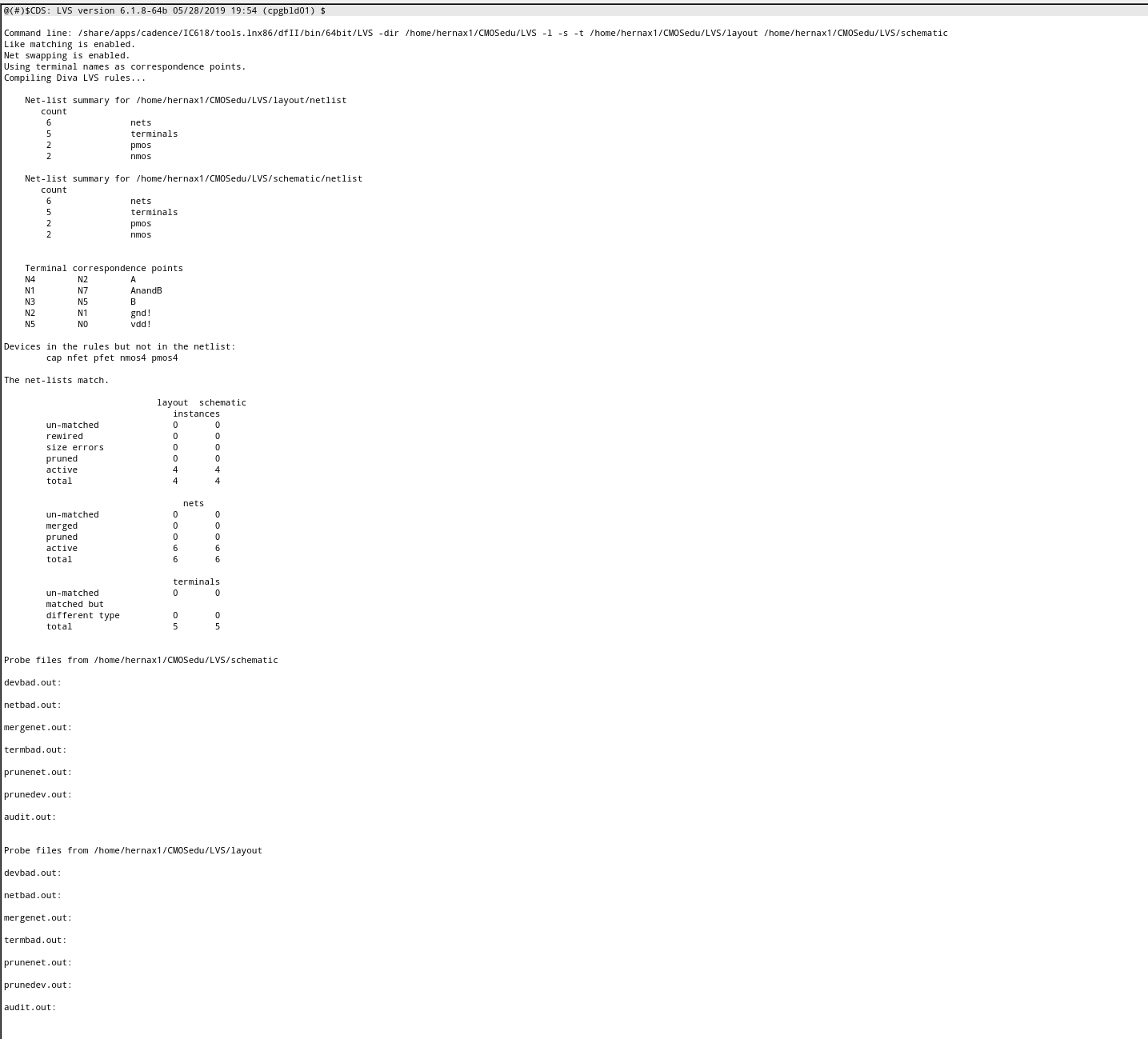
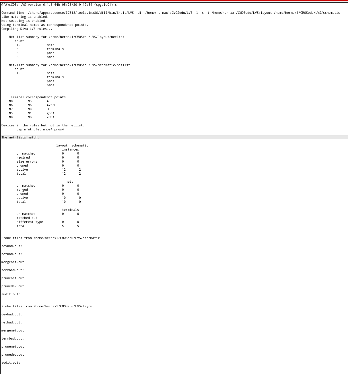
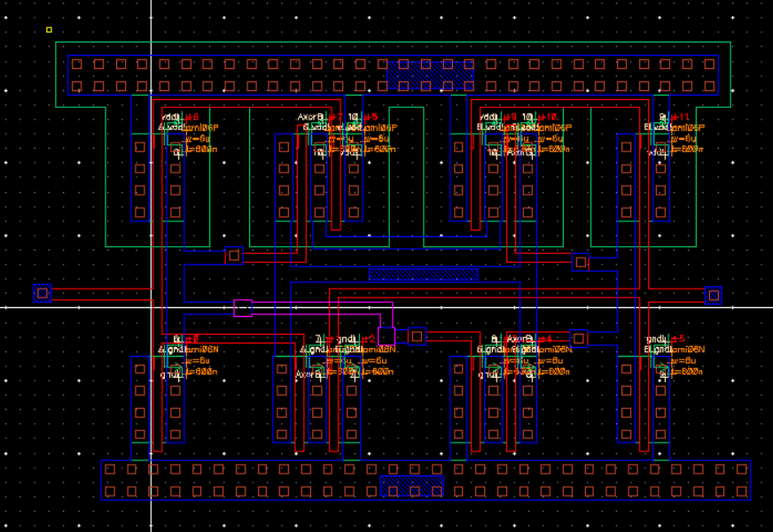
NAND Layout w/ DRC check and passing through LVS check.
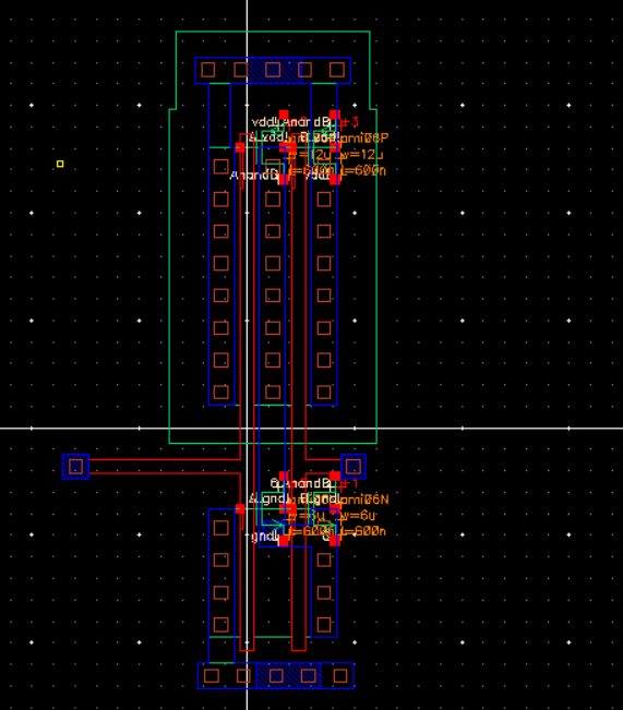
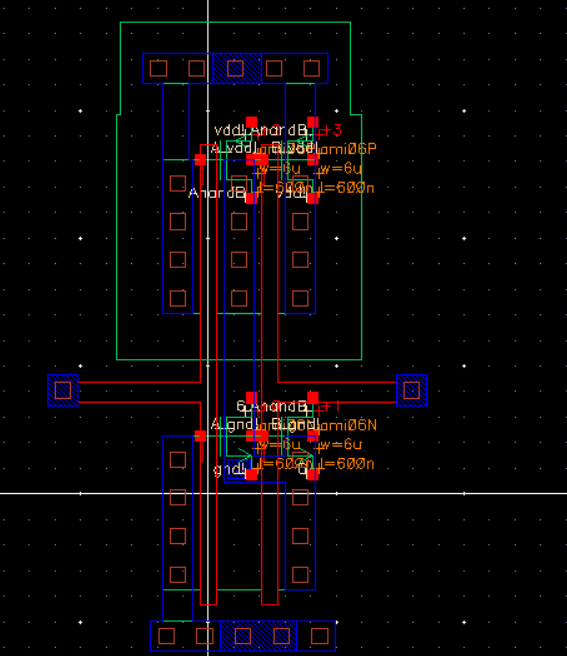
And finally the extracted NAND
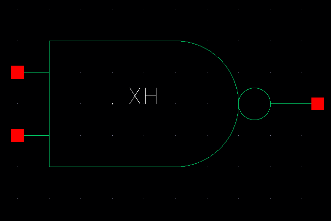
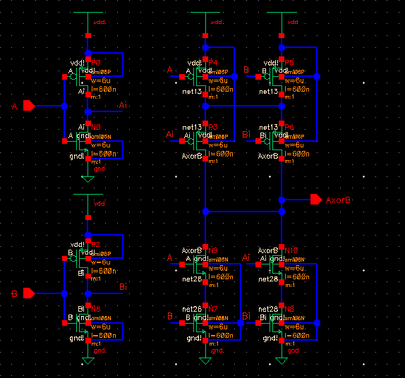
XOR gate
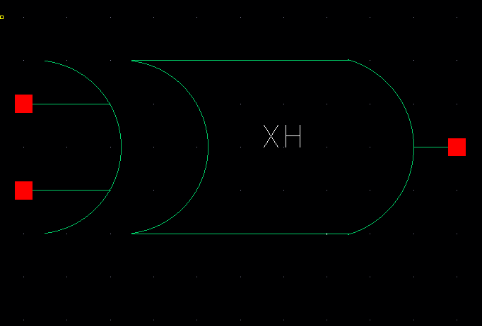
First we build the XOR schematic, and its corresponding symbol
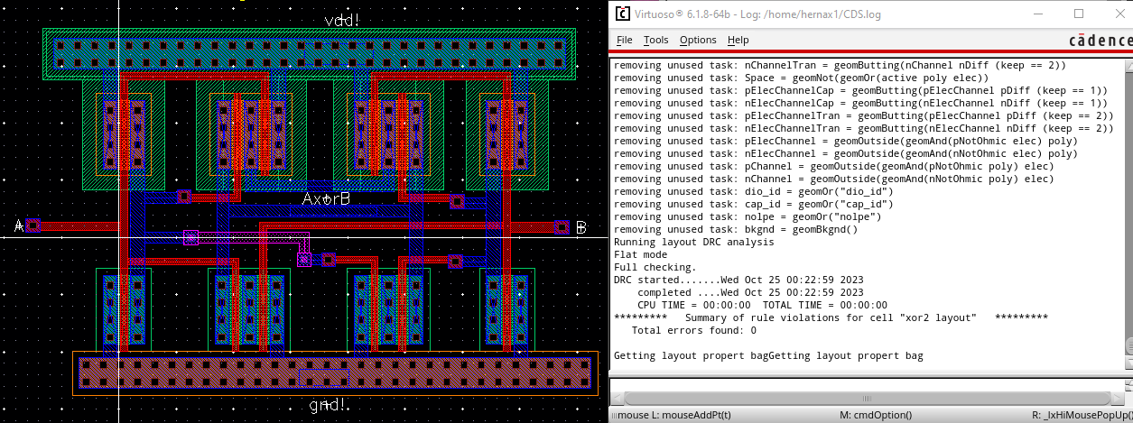
Extracted:
XOR/NAND Simulations
Using these gates, we can then observe the simulations for the inputs of: 00,01,10,11
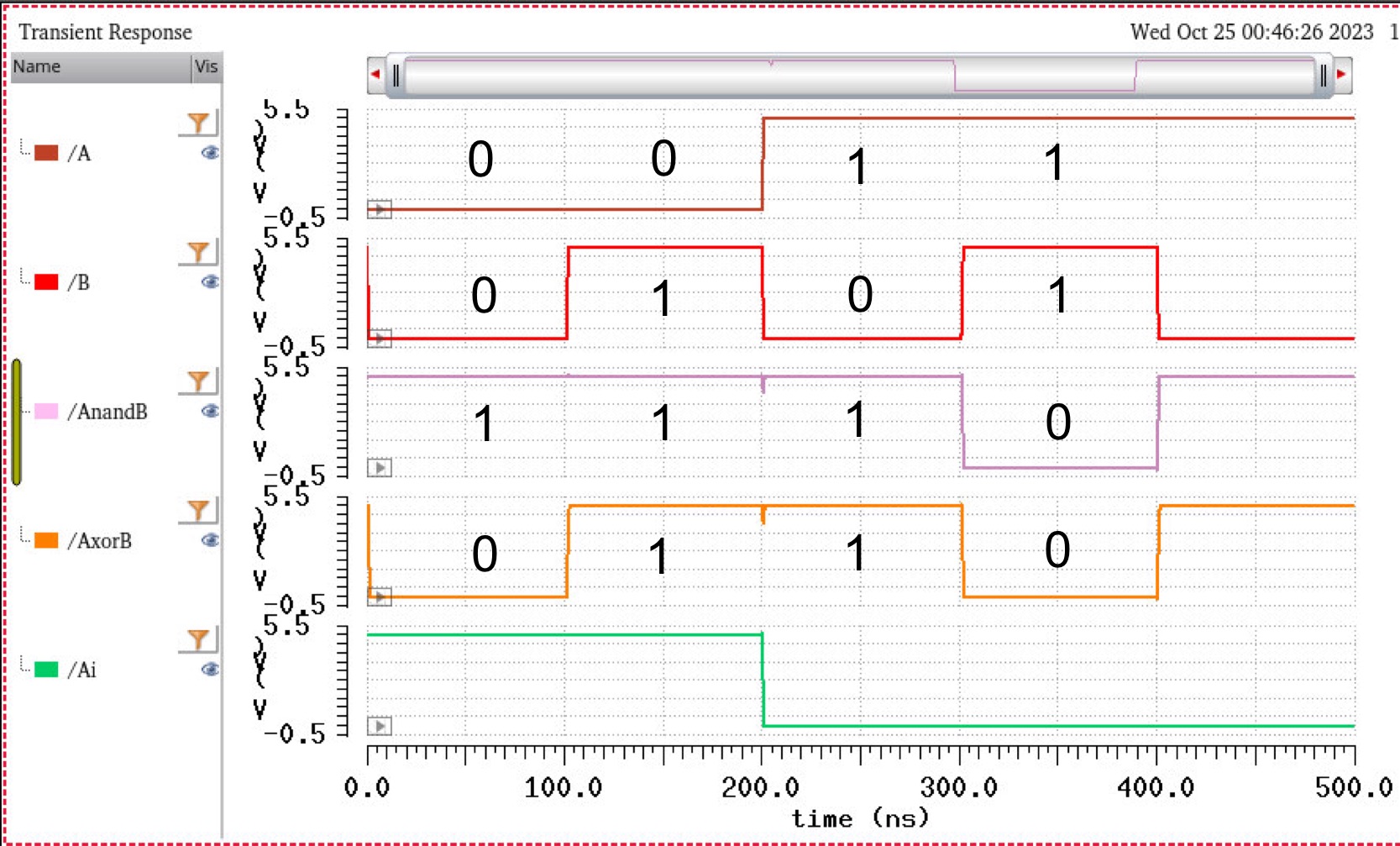
Which gives us the following tables
| A | B | AnandB | AxorB |
| 0 | 0 | 1 | 0 |
| 0 | 1 | 1 | 1 |
| 1 | 0 | 1 | 1 |
| 1 | 1 | 0 | 0 |
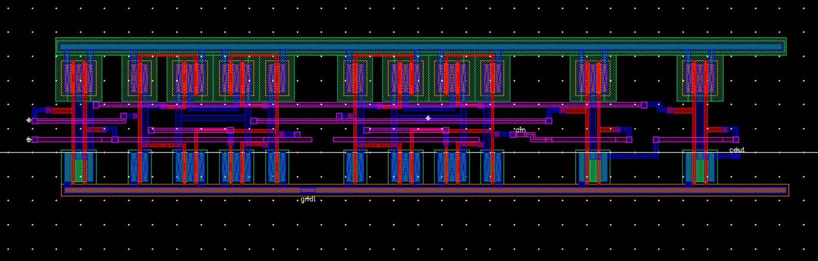
Full-adder
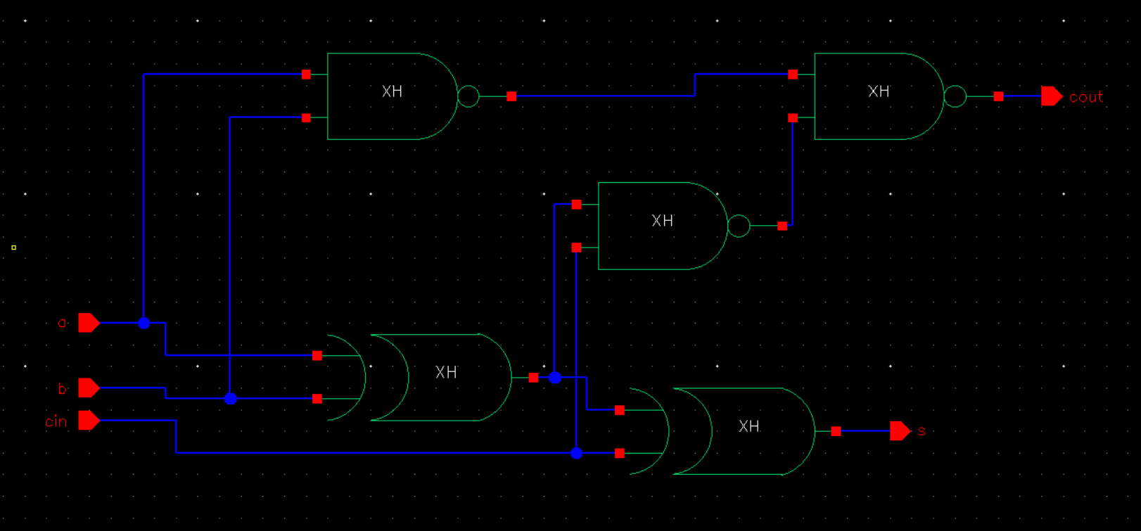
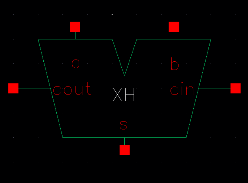
First we create the full-adder schematic and symbol
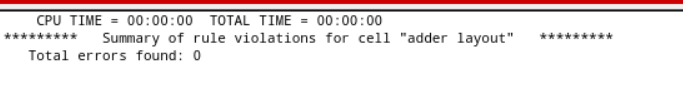
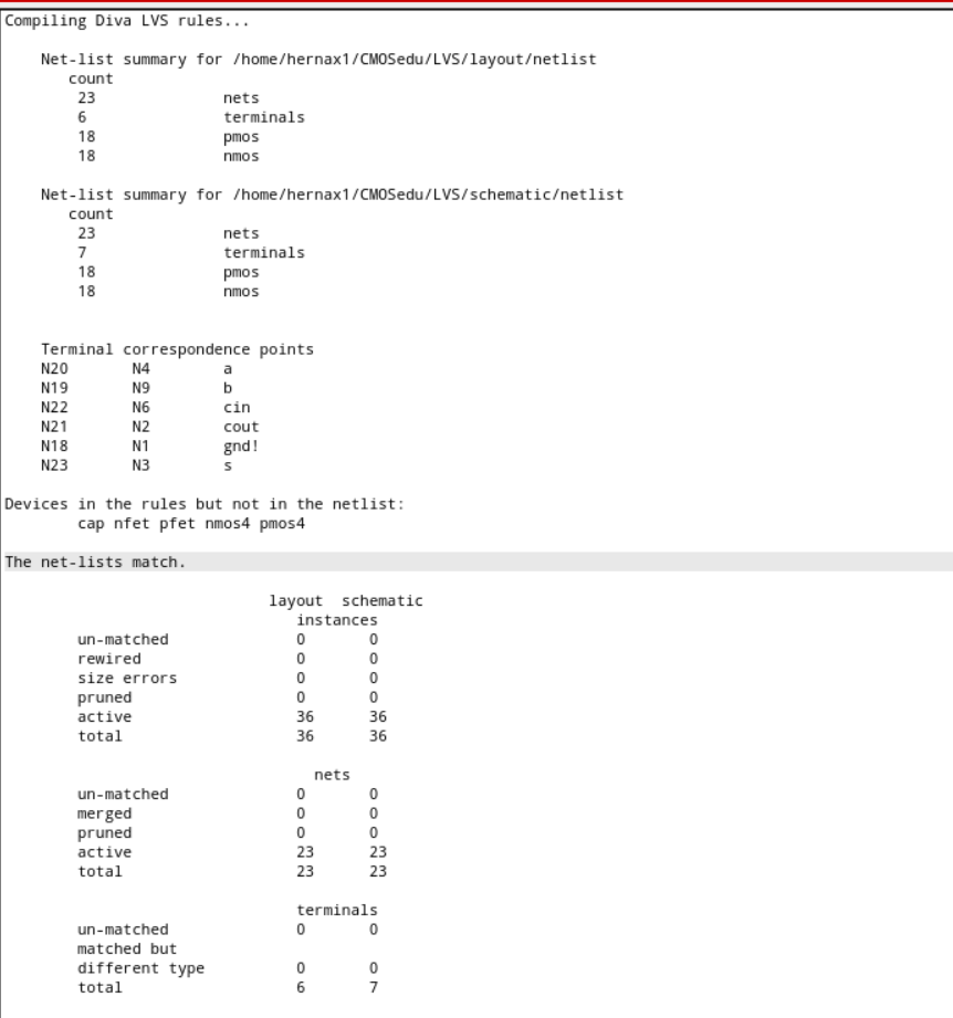
Next we create the full-adder layout, then DRC and LVS check.
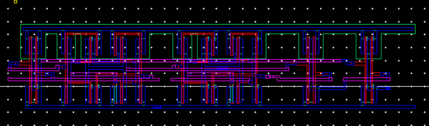
Extracted full-adder:
Finally, we simulate our full-adder for all possible inputs
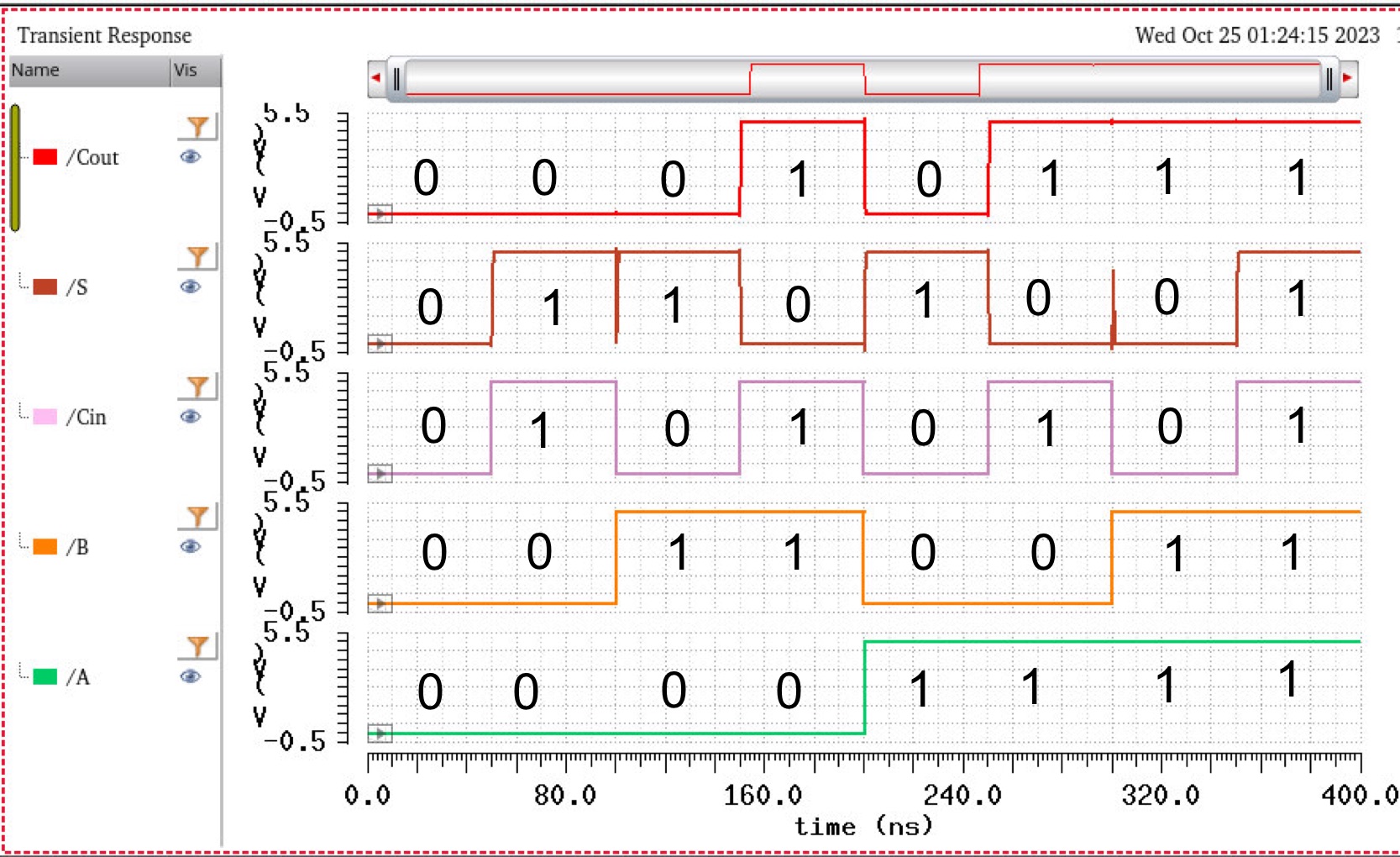
Which can then be converted to this table below.
| A | B | Cin | S | Cout |
| 0 | 0 | 0 | 0 | 0 |
| 0 | 0 | 1 | 1 | 0 |
| 0 | 1 | 0 | 1 | 0 |
| 0 | 1 | 1 | 0 | 1 |
| 1 | 0 | 0 | 1 | 0 |
| 1 | 0 | 1 | 0 | 1 |
| 1 | 1 | 0 | 0 | 1 |
| 1 | 1 | 1 | 1 | 1 |
Finally, as always, work getting backed up
Return to Xavier's Labs
Return to EE421 Labs