Lab 4 - ECE 421L

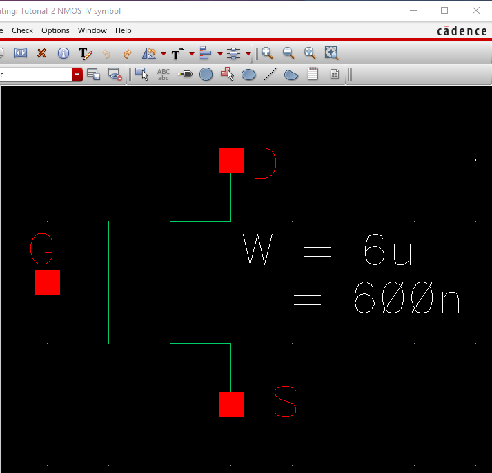
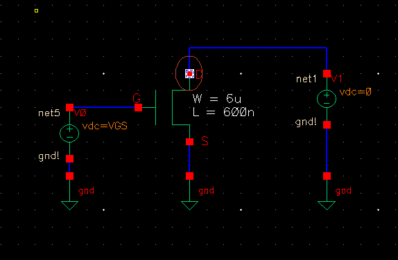
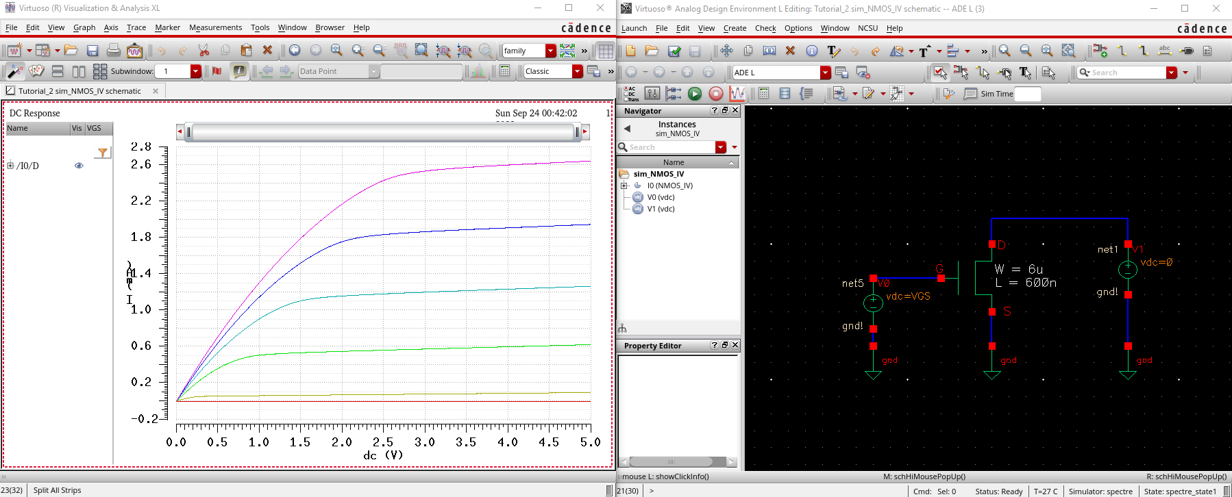
We then move on to create another cell called sim_NMOS_IV_3 and we instantiate the symbol that we created above. We also add wiring and 2 DC voltage sources, leading to our circuit below.
Left voltage source: V0=VGS , this will vary in our simulations (ex: V0=VGS, V0 = 2VGS, V0 = 3VGS, and so on...)
Right voltage source:V1=0
We move on with creating our layout of our nmos schematic. The tutorial takes us through a few steps of designing a layout that ends up failing LVS check when we test our extracted layout vs the schematic we made earlier. The reasoning for the LVS fail is due to the layout actually having 4 terminals (G, D, S and... B) but we only called out 3 of the terminals. We usually assume the p-substate is tied to gnd!. However, virtouso doesn't make this assumption and we must call out the terminal directly in the layout in order to satisfy the errors.
So we edit our layout to include the 4 connections WITH the p-sub directly called out to gnd!, and the resulting layout is seen below.
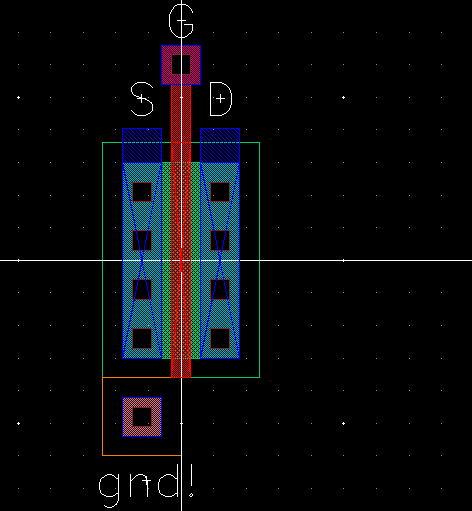
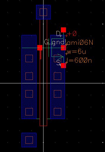
We then extract our layout and get this below. As we can see, we have all the terminals directly called out.
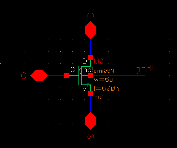
If we try to run LVS again, we will once again have errors, notice that our layout has 4 terminals, whilst the original schematic we created at the beginning only has 3 terminals (B is not included). So we must go back to our schematic and redesign it to match what our new 4 terminal nmos layout is.
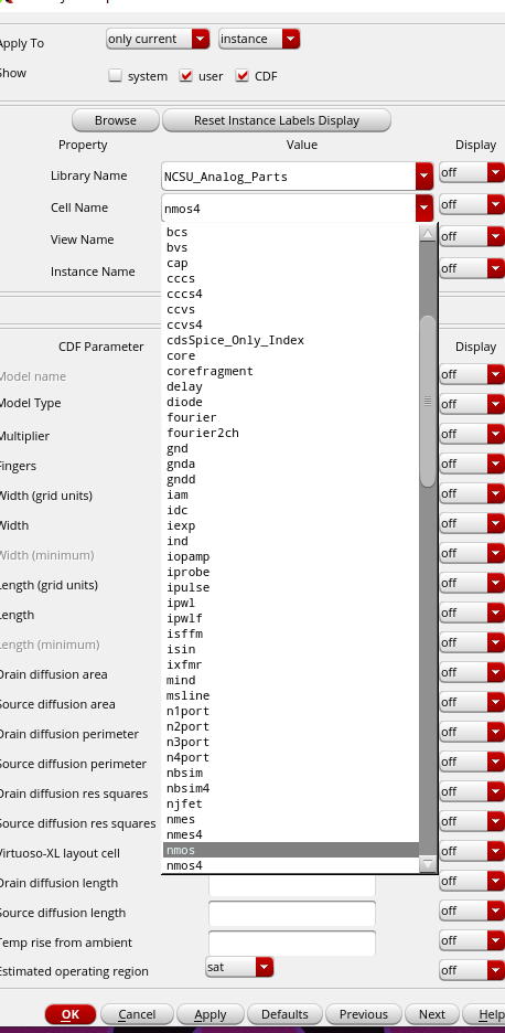
We first change our NMOS symbol from nmos -> nmos4,
Then we add a gnd! wire with a label, our new schematic is seen below.
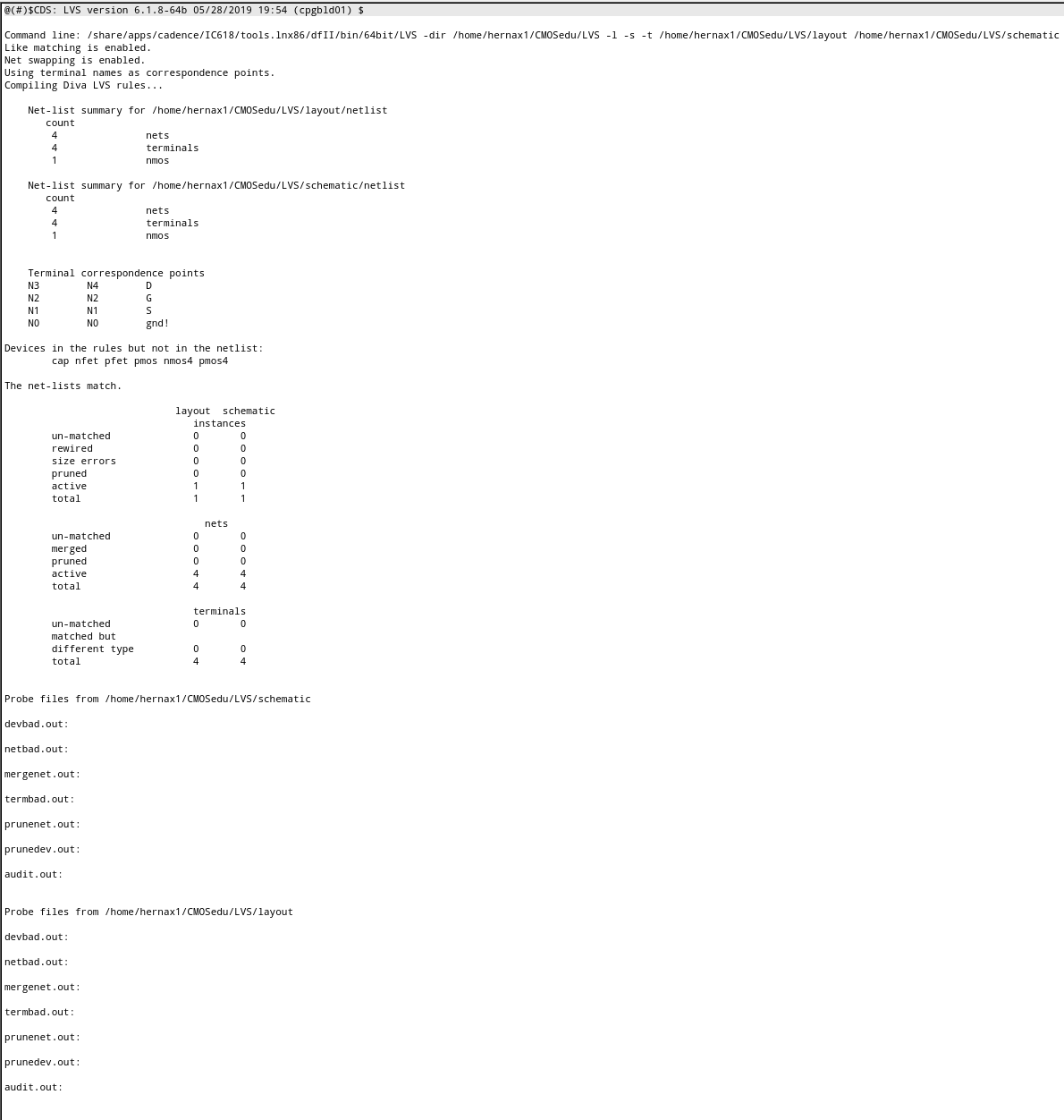
We can now finally LVS check the newly created schematic above, with the extracted layout that we created. The results are below with netlists matching.
We want to test that our extracted layout actually works, so we once again return to our simulation.
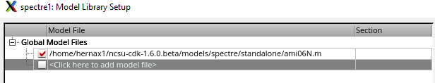
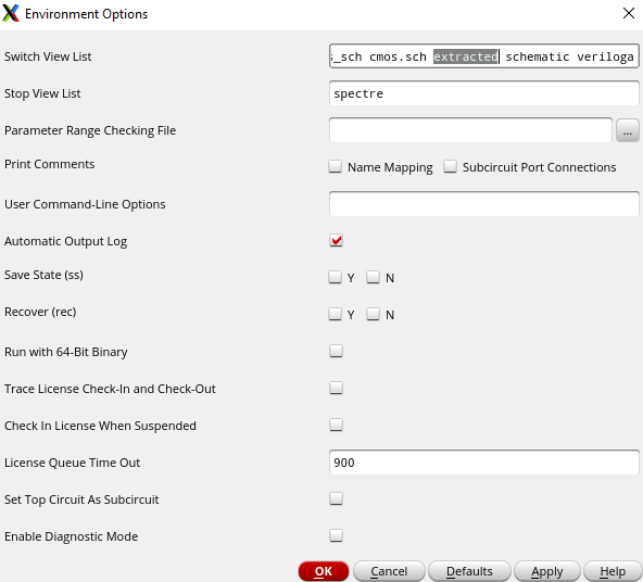
We go to Setup -> Environment and add extracted before schematic so that we use the extracted layout to run our sim.
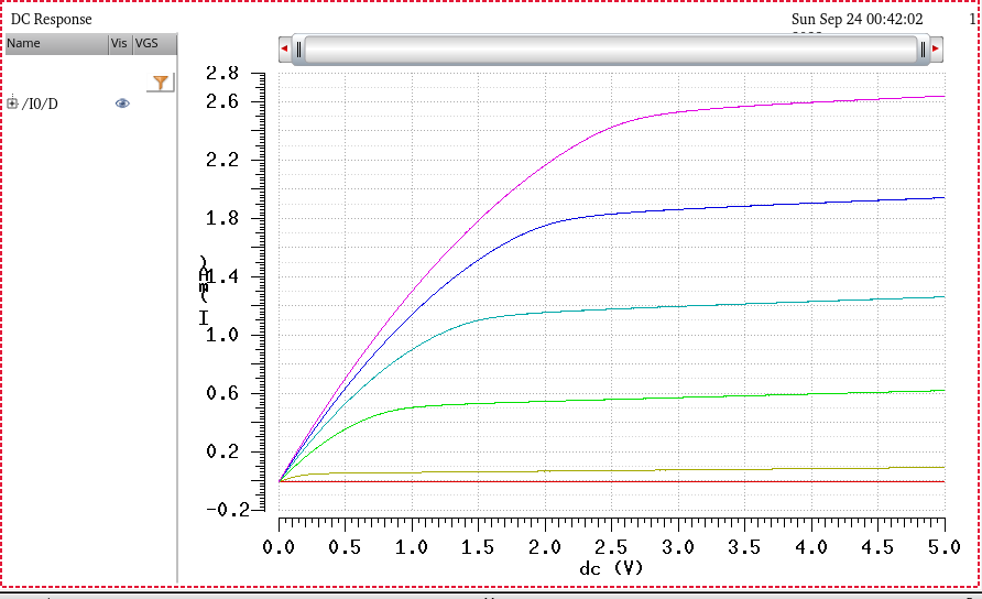
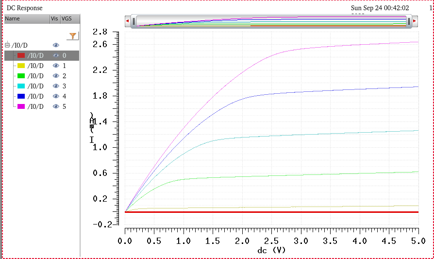
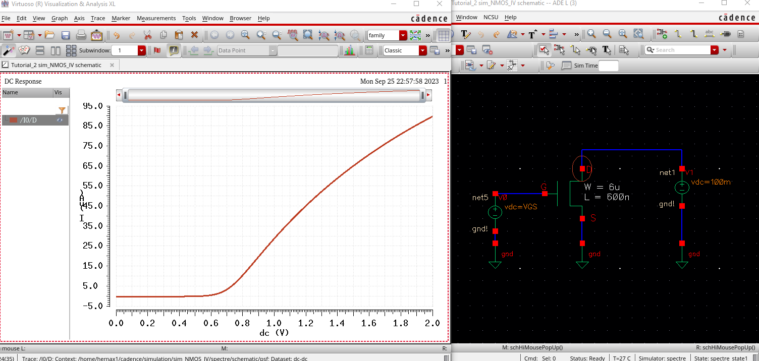
We then do the exact same process as how we simmed before and we get these results below. Which are the same as the previous simulation.
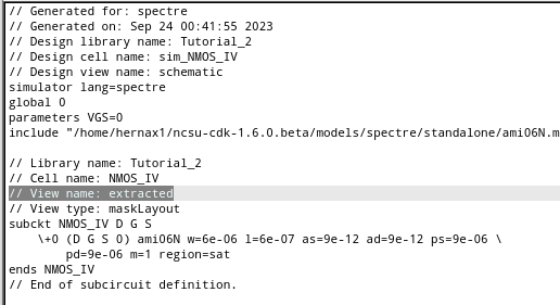
And once again, to prove that extracted view was used to simulate, the netlist seen below.
Now for the next part, we repeat the same process but we will sim and layout a PMOS.
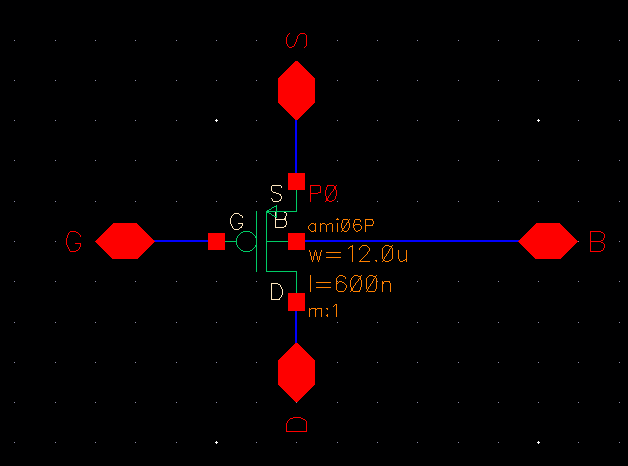
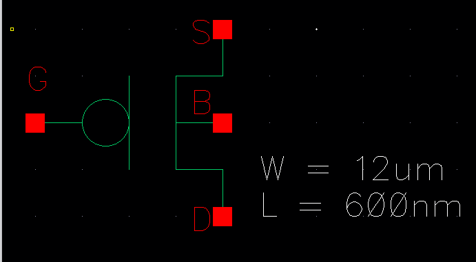
First, we create the PMOS schematic below with W = 12um and L = 600nm.
Then we create our symbol for the schematic.
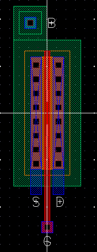
Next we make our layout for the PMOS.
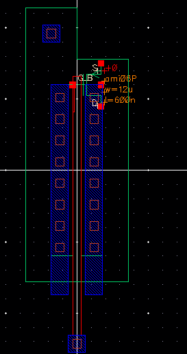
Then we extract our layout.
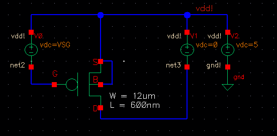
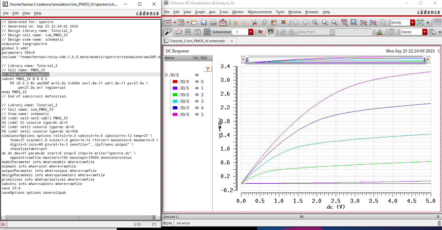
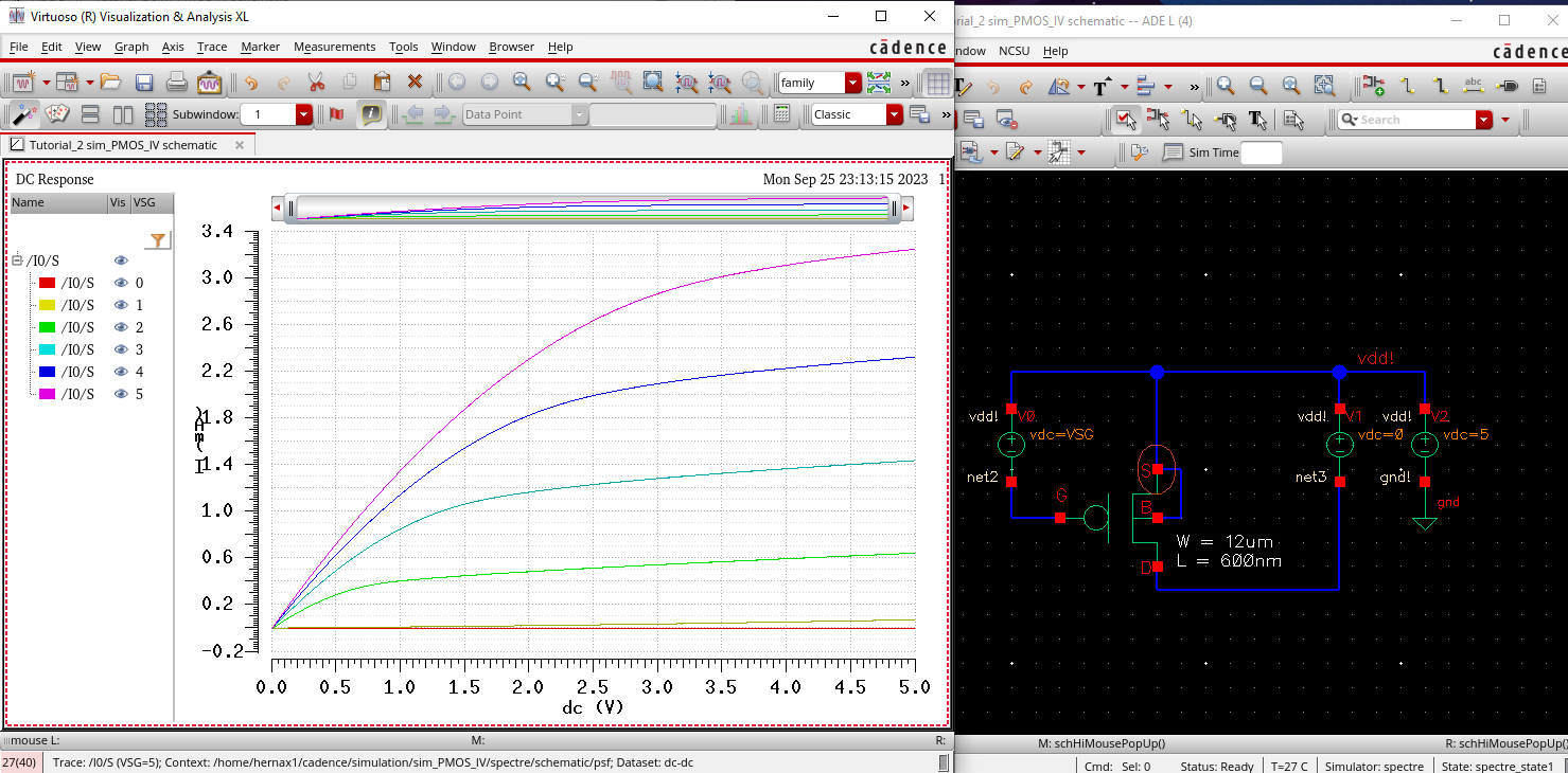
We move on to simulations of our PMOS. We create the schematic below in a new cell sim_PMOS_IV.
Finally, we can simulate the design, using similar setup process like the NMOS. Below are the results using the schematic in the simulation.
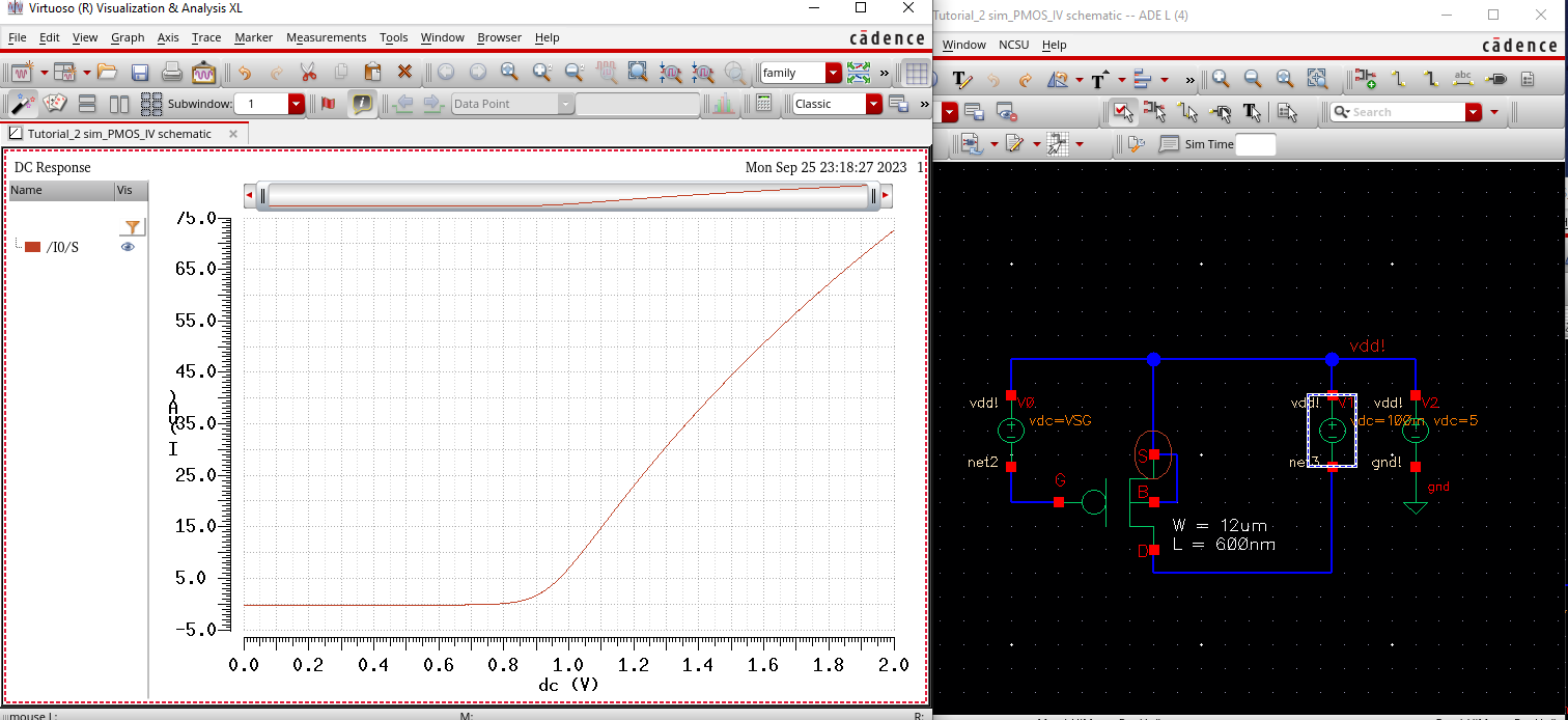
Next are the results when simming with our extracted layout.
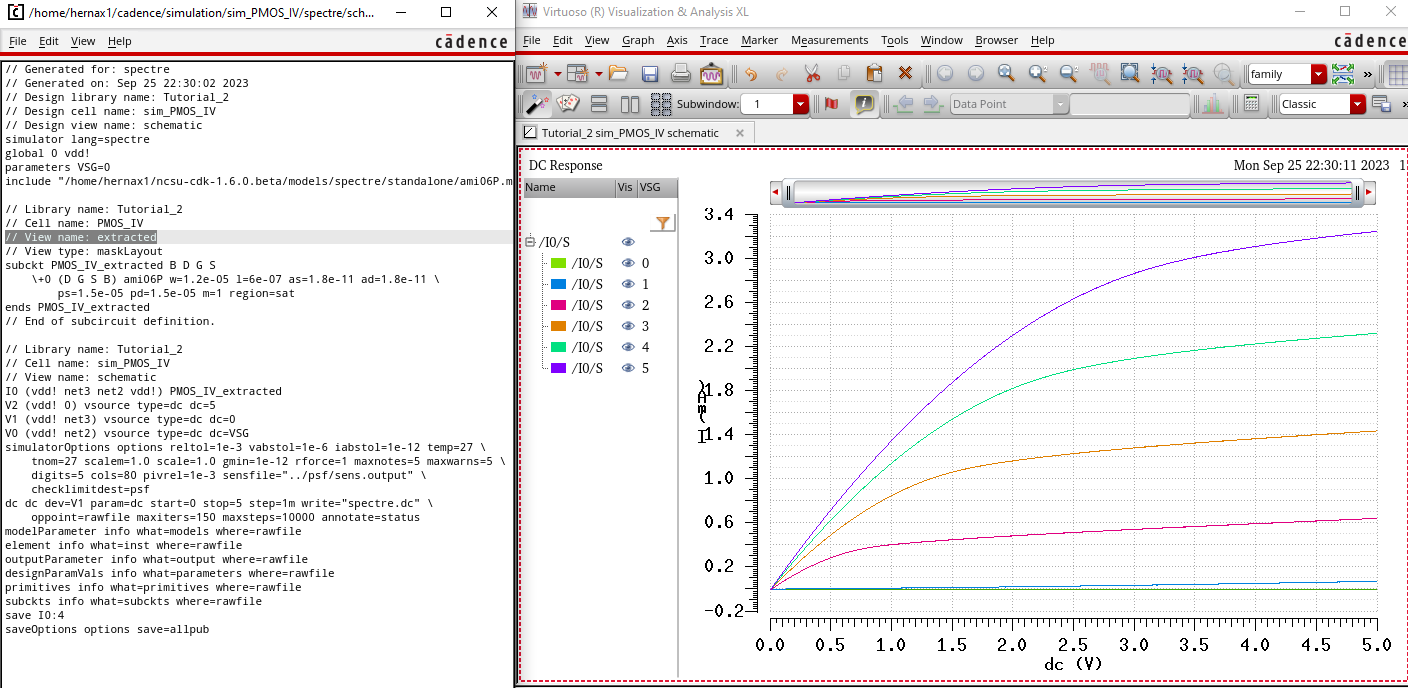
As you can see, both the schematic and extracted simulations provodie the exact same sim results, showing the layout of our PMOS was done correctly.
Thus concluding tutorial 2 and prelab work.
Labwork
We are tasked with generating the 4 schematics and simulations for the 4 different IV curves.
Where VDS varies from 0 to 5V in 1mV steps
VGS varies from 0 to 5V in 1V steps
Width = 6um and Length = 600nm.
Where VDS = 100mV constant.
VGS varies from 0 to 2V in 1mV steps.
Width = 6um and Length = 600nm
Where VSG varies from 0 to 5V in 1V steps
VSD varies from 0 to 5V in 1mV steps.
Width = 12um, Length = 600nm.
Where VSG varies from 0 to 2V in 1mV steps
VSD = 100mV constant.
Width = 12um, Length = 600nm.
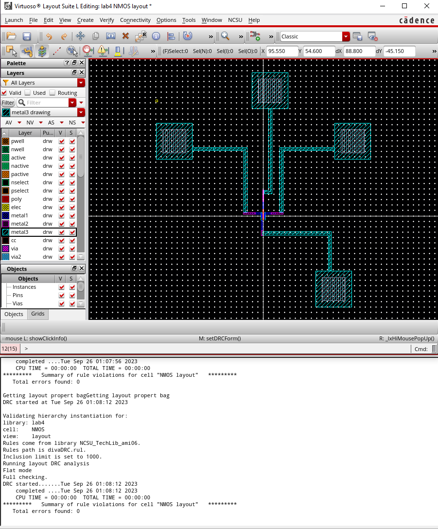
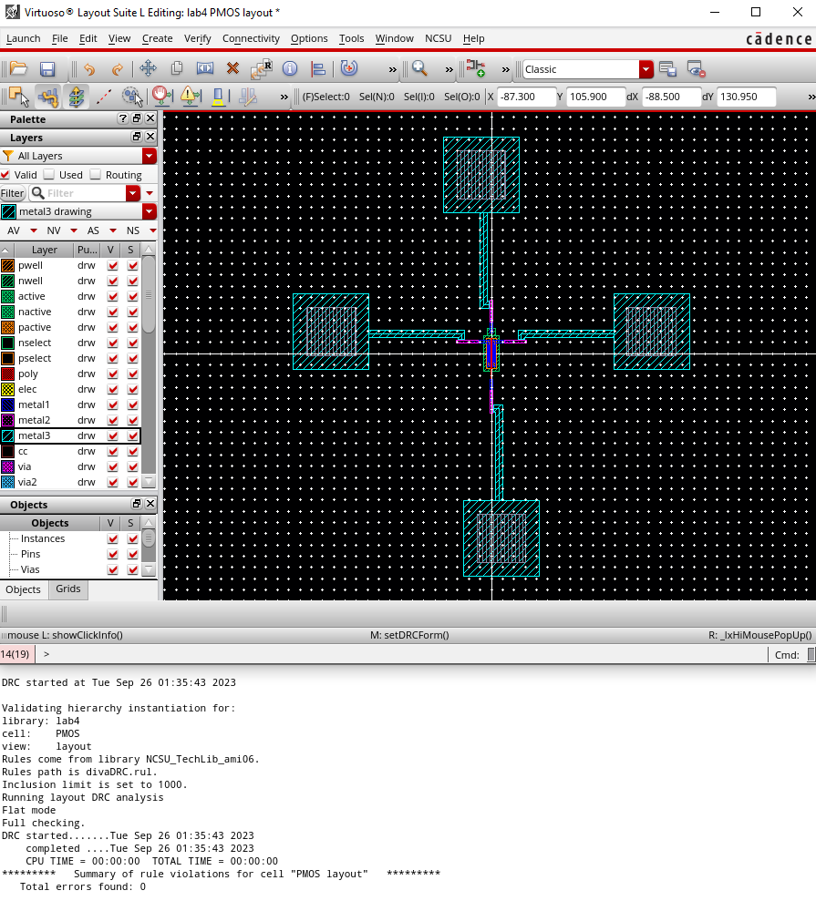
Below is the layout of NMOS with 4 probe bads, followed by the DRC check with 0 errors.
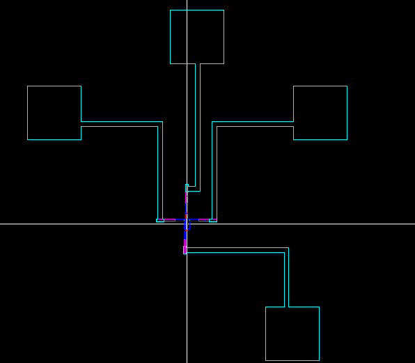
After we confirm DRC check passes, we extract the layout.
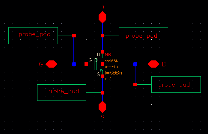
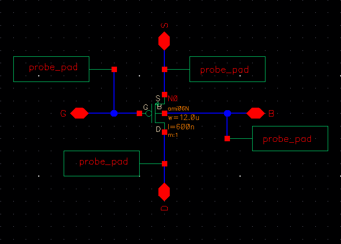
We design a NMOS schematic with probe bads in order to check LVS
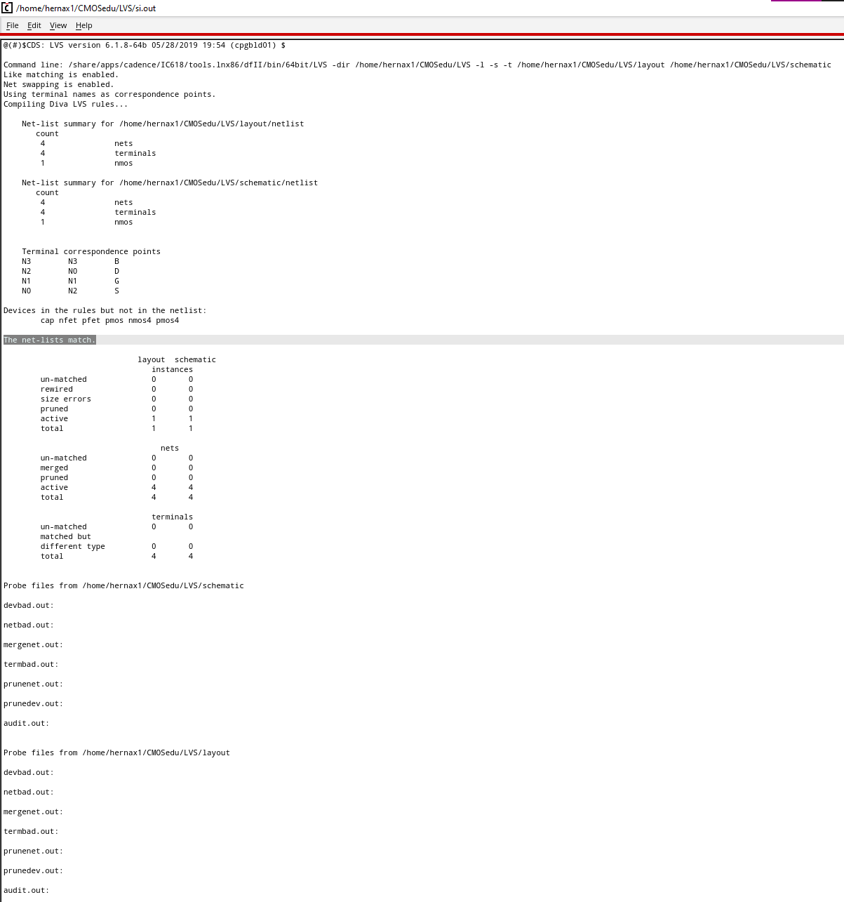
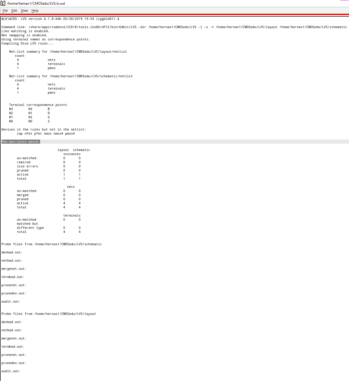
Then we run LVS with our extracted layout and our newly created schematic, and we get the results below, netlists match,
Below is the layout of the PMOS with the 4 probes. DRC check is included as well, 0 errors.
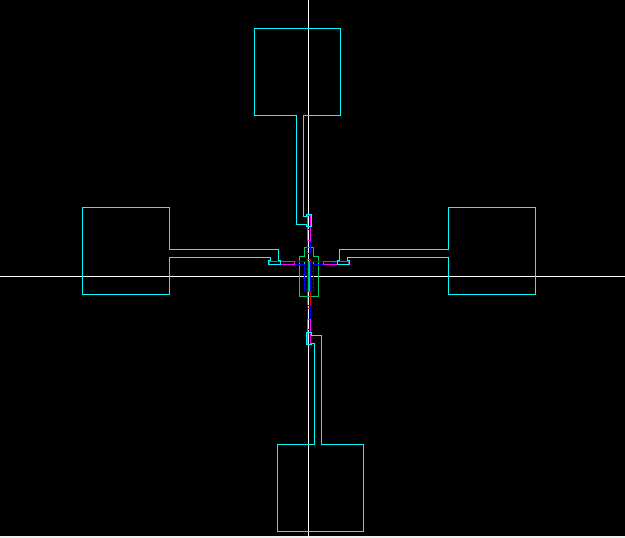
Once DRC check passes, we extract the layout and get this extracted view.
Now, we make a schematic of our PMOS including probes so that we can run LVS, the schematic of the PMOS is below.
Finally, we LVS with our newly created PMOS schematic and our extracted layout. Seen below, the netlists match.
Return to Xavier's Labs
Return to EE421 Labs