Lab 2 - ECE 421L
Authored
by Xavier Hernandez,
9/5/23
Pre-lab Work
- How is the input voltage, Vin, related to B[9:0] and Vout?
Vin
is related to Vout and B[9:0] by converting the AC analog input (Vin)
into a staircase binary output(Vout) that has output steps based on the
number of bits (B[9:0]).
We have 10 bits for this simulation, which is used to calculate the LSB. Vout will end up being a less accurate representation of Vin due to the low number of bits.
To begin our prelab setup, we download the lab2.zip file and add it into the CMOSedu directory, then unzip it.
Then we add this statement into cds.lib DEFINE lab2 $HOME/CMOSedu/lab2.


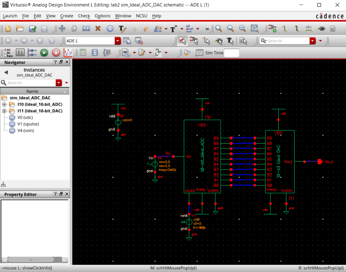
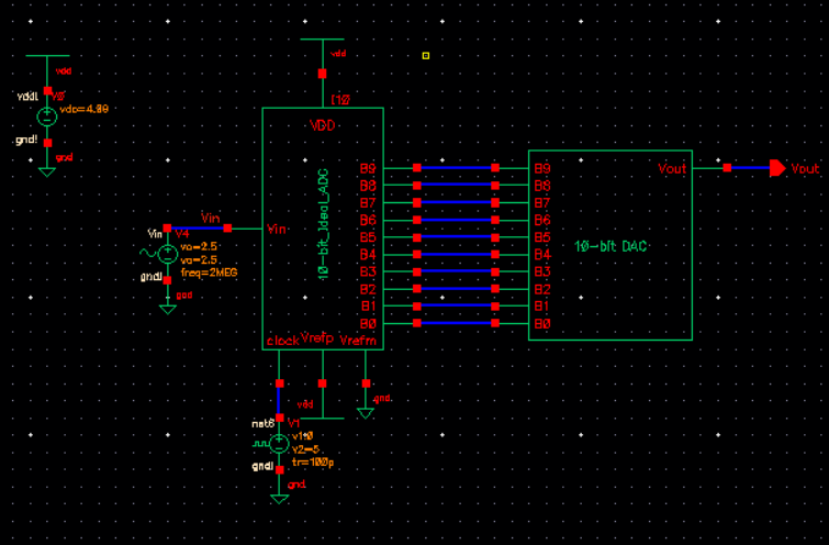
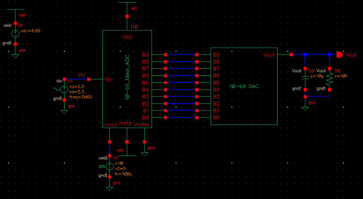
After that setup, we launch Cadence, then we locate and open the correct file in the library manager: lab2 -> sim_Ideal_ADC_DAC -> schematic.
Which then brings up the following schematic, second image below.
After that, we can simulate, we launch ADE L, and load the spectre simulation using: Session -> Load State -> Cellview.
Which brings up the following simulation results.
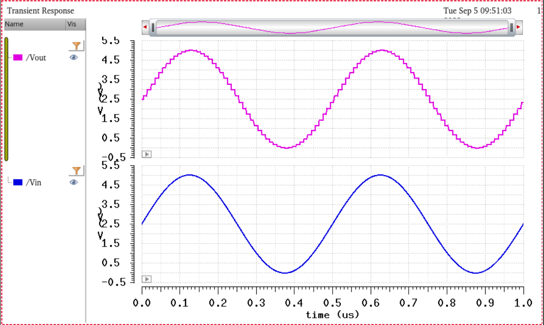
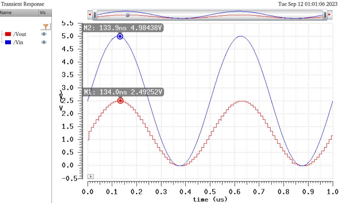
As seen above, Vout has a non-smooth staircase waveform that would be greatly improved if the number of bits was increased.
- Different Simulation Results
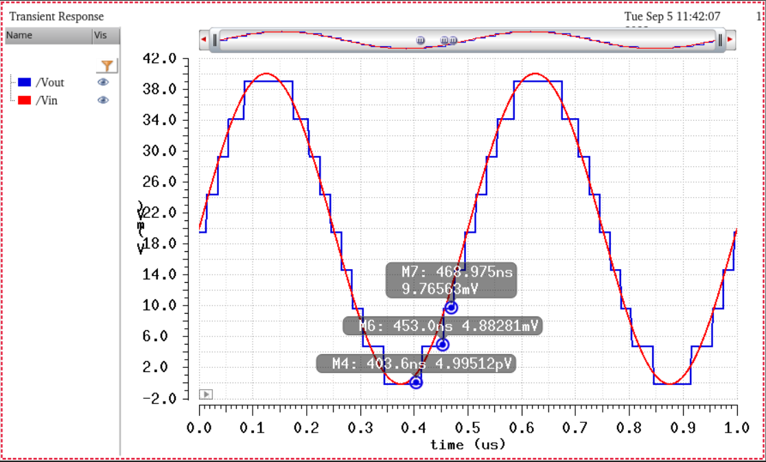
So seen below, where Vin input has an amplitude of 20mV, and an offset of 20mV so that we can see the steps of Vout.
This smaller voltage allows us to see the output steps more clearly.
Marker 4(Vout) is 0V as expected, since Vin is between 0 and 2.44mV.
Marker 6(Vout) is 4.88mV, where Vin is between 2.44mV and 7.32mV.
Marker 7(Vout) is 9.76mV, where Vin is between 7.32mV and 12.2mV.
- Determine the Least Significant Bit.
Essentially, the output step possible (Least Significant Bit) is determined by this equation.
Where Vdd = 5V and n = 10, leading to LSB = 4.88mV. So each output step is 4.88mV.
After which, we can halve it (2.44mV) to determine the ranges of Vin that will round the output to a higher or lower step.

For example:
if Vin = 0 to just under 2.44mV, then Vout = 0V;
if Vin = 2.44mV to just under 7.32mV, then Vout = 4.88mV;
if Vin = 7.32mV to just under 12.2mV, then Vout = 9.76mv.
And so on until we reach our peak Vin.
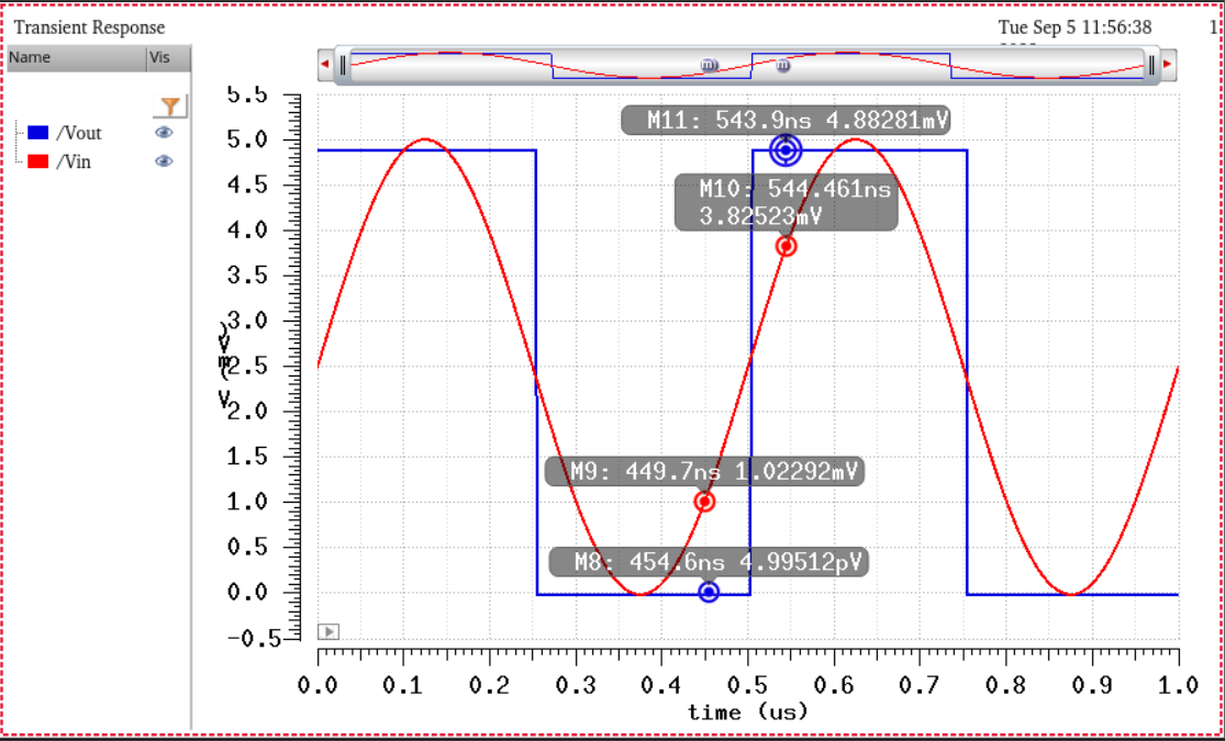
Seen below we can clearly see the LSB,
where Marker 9 (Vin = 1.02mV) and Marker 8 (Vout = 0V) are related, Vin is in the range of 0-2.44mV so Vout = 0V.
and
Marker 10 (Vin = 3.82mV) and Marker 11 (Vout = 4.88mV) are related, Vin
is in the range of 2.44mV to 7.32mV so Vout = 4.88mV.
Lab work
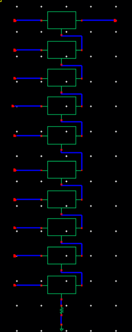
- Design of 10-bit DAC using an n-well resistor of 10k
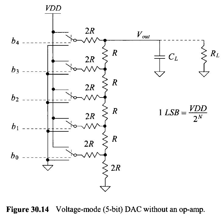
To
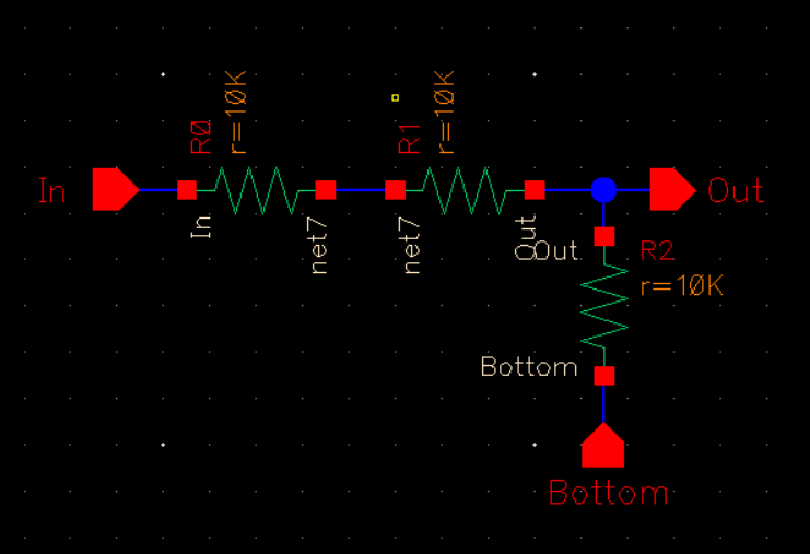
begin, we create a voltage divider that copies Fig 30.14, where 2R is on
the left of the divider and is 20k ohms and on the right of the divider, R with 10k
ohms.
Then attach the "in, out and bottom" pins,
Then we can create the symbol below that will represent one bit. We will be needing 10 of these to create the DAC
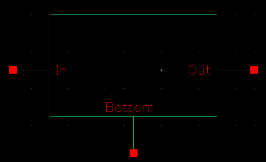
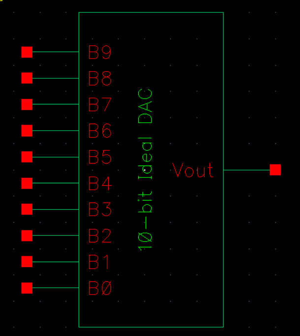
- Creating Symbol View of the DAC
Then
we create the symbol with the same footprint as the given Ideal DAC
symbol; to do this, we copy the the cell over from the
"Ideal_10_bit_DAC" and edit the symbol's schematic. We could have made our own symbol but the lab specified to have our DAC be the same dimensions.
First, the symbol's schematic is edited; below using 10 of the "1-bit" respresenations and a 10k ohm resistor at the very bottom, we can create the 10-bit DAC which has the same layout as Fig 30.14.
Then,
below is the edited symbol completed with the correct dimensions and
the updated pins from the schematic edit. Vdd and Vref+/Vref- are
removed as they will not be used for this design.
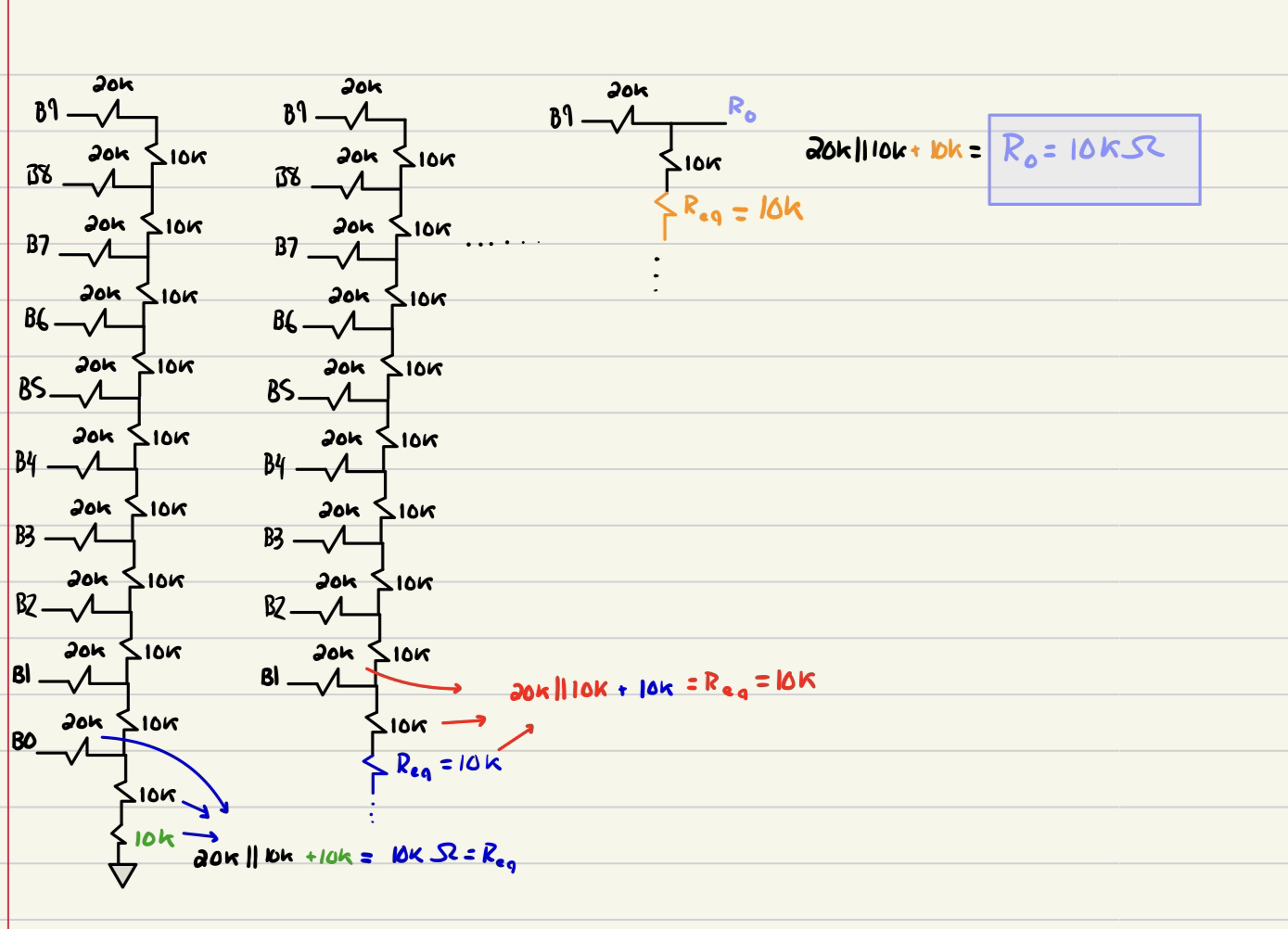
- Output Resistance of the DAC
To
calculate the output resistance, we begin at the very bottom of our
schematic. Where 10k = R and 20k = 2R (via lab instructions).
First we find the equivalent parallel resistance of the two 20k ohm resistors, the new resistance we get is 10k(which
is R). That new equivalent resistance is now in series with the next
10k resistor, so now we once again have two 20k ohm resistors in
parallel. This calculation repeats up until we reach the top of our DAC
where we once again do the same thing and get an output resistance of
10k ohms, (R=10k ohms).
Using
the approximation of "td = 0.7RC", where we have an RC circuit, with a
capacitor of 10pF, we can approximate the time delay:
td = 0.7 * (10k) * (10p) = 70ns
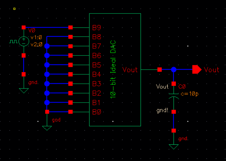
Further
more, we can verify this time delay with the simulation below, where we
ground all bits except B9, and add the capacitor load. Schematic
circuit on first image, sim result on the second. Where we go from 0
-> VDD (VDD = 5V, from the Ideal ADC to DAC schematic).
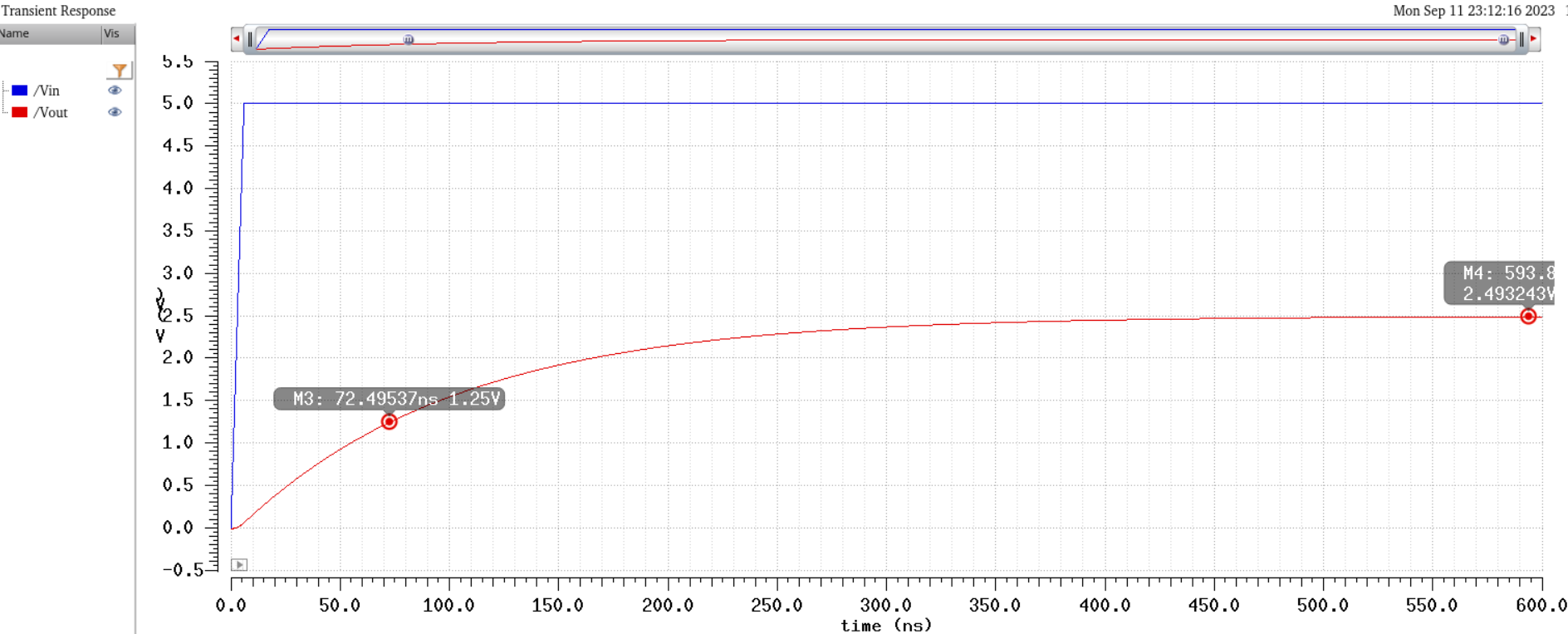
Seen
below is the time delay for when the voltage across the capacitor
reaches 1.25V, which is half of it's max value, in this case 2.5V is
the max voltage possible across the capacitor. The time delay measurment is 72ns when recorded via sims,
close to the 70ns approximation calculated above. The marker on the
right shows the capacitor approaching it's max value of 2.5V.
- Simulations to Verify Design
First Simulation: No Load
As expected, the simulation output behaves the same as the Ideal_DAC that was simmed in the prelab.
Using VDD = 4.99V saved my simulation.
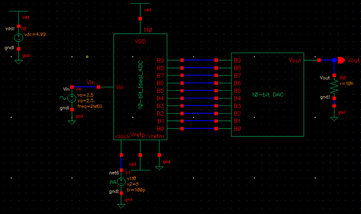
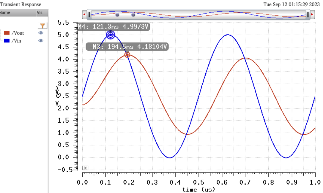
Second simulation: Resistive Load
Connecting
a 10k ohm load. As we know from previous calculations, the output
resistance is R for this 10-bit DAC (R = 10k ohms for this lab). Now
since we are introducing this second 10k ohm resistor load, we have now
created a voltage divider where output will always be 1/2 the input,
clearly seen below, where the output is roughly 2.5V.
10k ohm load connected on the right.
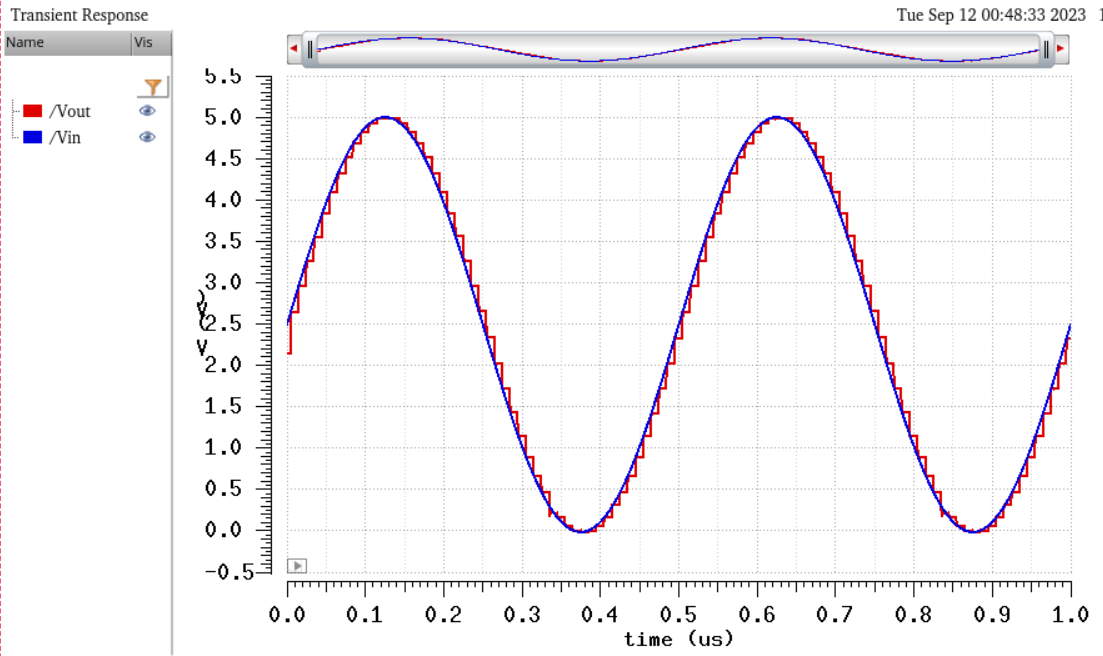
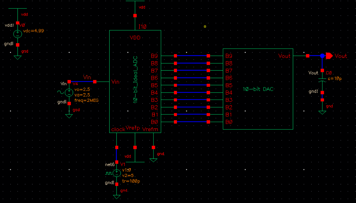
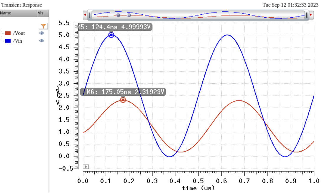
Third Simulation: Capacitive Load
Using
the previously used value of 10pF. We can see the output wave is
drastically smoothed. Additionally we now notice that the output has a
time delay and a new DC offset. As we knew previously, the 10pF
capacitor had a 72ns time delay, when connected in an RC circuit.
Since the capacitive load is acting the same in this circuit,
with output resistance of R = 10k ohms, then we can likewise see
below that Vout experienes the same behavior and has a similar lag time
of 73ns behind Vin. Additionally the DC offset appears to be between
roughly 4.1V to 1.1V with a DC offset of 2.6V.
Capacitive load on the right.
Fourth Simulation: R/C Load
Now
the combination of the resistor and capacitor in parallel has caused
our output to be smooth and act as a voltage divider, along with having a time
delay.
Below we see that the time delay for Vout is about 50ns, and
Vout is slightly under 1/2 voltage of Vin, 2.3V. DC offset appears to
have been drastically minimized.
10k ohm resistor and 10pF capacitor in parallel load.
In
a real circuit the switches seen above (the outputs of the ADC) are
implemented with transistors (MOSFETS). Discuss what happens if the
resistance of the switches isn't small compared to R.
If
the
resistance of the switches isn't small, then we have to take
those resistance values into the consideration of our output
resistance(we previously calculated it as R through simple
calcs), this effects our output voltage since output resistance will no
longer be R. That means, the user would have to reasses the R value to
calculate a new resistance required in order to keep the DAC
working as intended.
Lab stuff getting saved and backed up.

Return to Xavier's Labs
Return to EE421 Labs