Lab Project - EE 421L
Authored
by Larri Gomez
gomezl6@unlv.nevada.edu
Project Description
We are to design a non-inverting buffer circuit that has an input capacitance less than 100 fF and
has an input logic where logic 0 would be 1V or less and logic 1 would
be 3V or more. The design should also work with a VDD between 4.5V and
5.5V. The design also will drive a varying capacitance from 0 to 1pF
and provide outputs from either 7V or more for logic 1 and near ground
for logic 0. The slowest transition time that is allowed is 4ns.
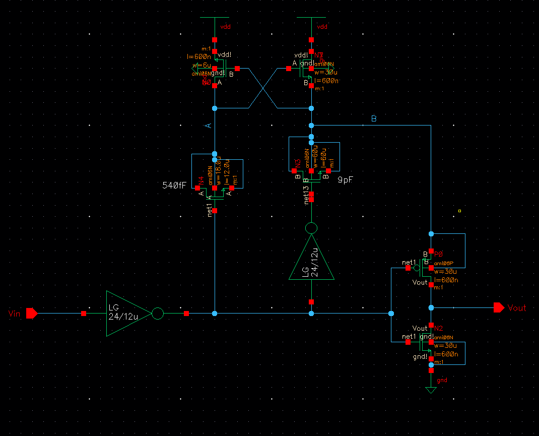
Project Desgin Overview
This
project will mainly make use of figure 18.39 from the textbook which is
a charge-pump clock driver. How this works is when a logic 0 is
inputted, then the first inverter will cause the input to go to 1 which
means node A will be high and node B will be low after going through
the second inverter. M2 would be on while M1 would be off meaning that
node A will be at 2VDD while node B will be at VDD. The PMOS and NMOS
receive the output from the first inverter which was logic 1 which
would make the PMOS power off and the NMOS power on. Since the NMOS is
connected to ground, the output of the driver will be roughly around
ground. Now if the input logic was now 1, the process would be the
opposite of how it was with logic 0. Node A will now be low with it
being at VDD and Node B going to high after going through the second
inverter making it 2VDD. In this case, the output of the first inverter
will be 0 meaning the the PMOS will be powered on and the NMOS will be
powered off. The output for logic 1 would then be from node B which is
2VDD. The main reason that a charge pump is being used for the
non-inverting buffer is to be able to drive the large outputs which for
our design, requires 7V or more.
Components Used with Specifications
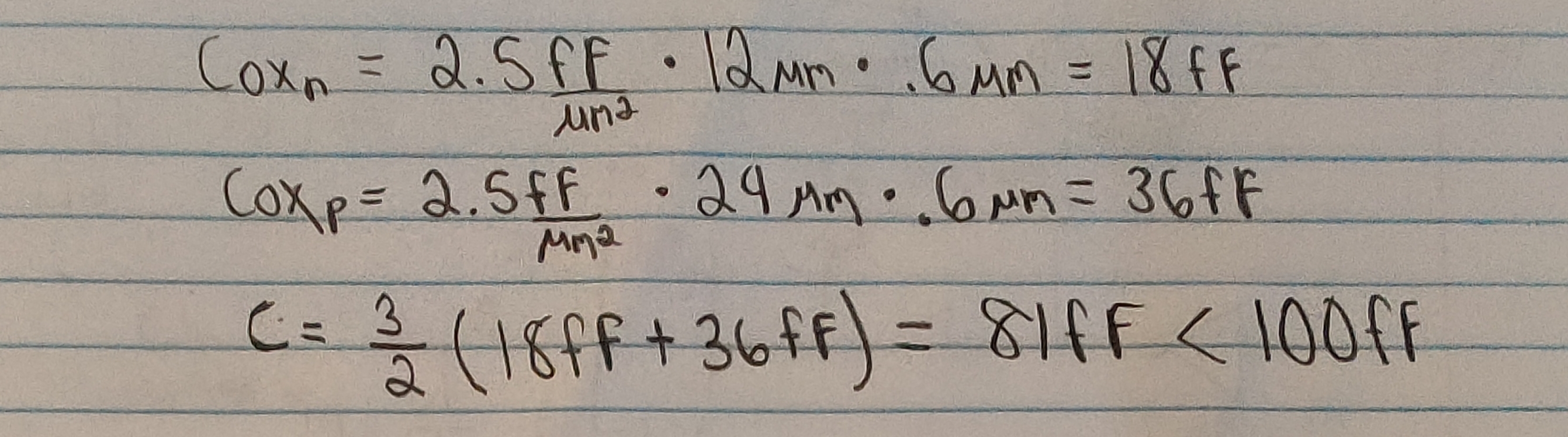
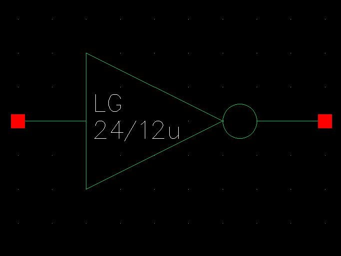
For the inverters,
I decided to use a 24u/12u inverter since the total input capacitance it provides is less than 100fF which can be
seen in the equation below.
For
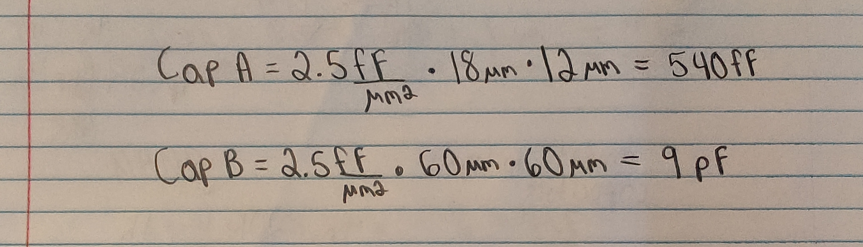
the capacitors,
I will be using shorted out NMOS devices as it will be easier to
layout. For the capacitor at node A, since it is only being used to
power M2 on, is does not have to be that big which is why I decided to
go with 540 fF which I got with my NMOS sized at 18u/12u. The capacitor
at node B has to be larger as it is responsible for supplying the
charge to the load which is why I decided to go with 9pF which I got
with the NMOS sized at 60u/60u. The calculations can be seen
below.
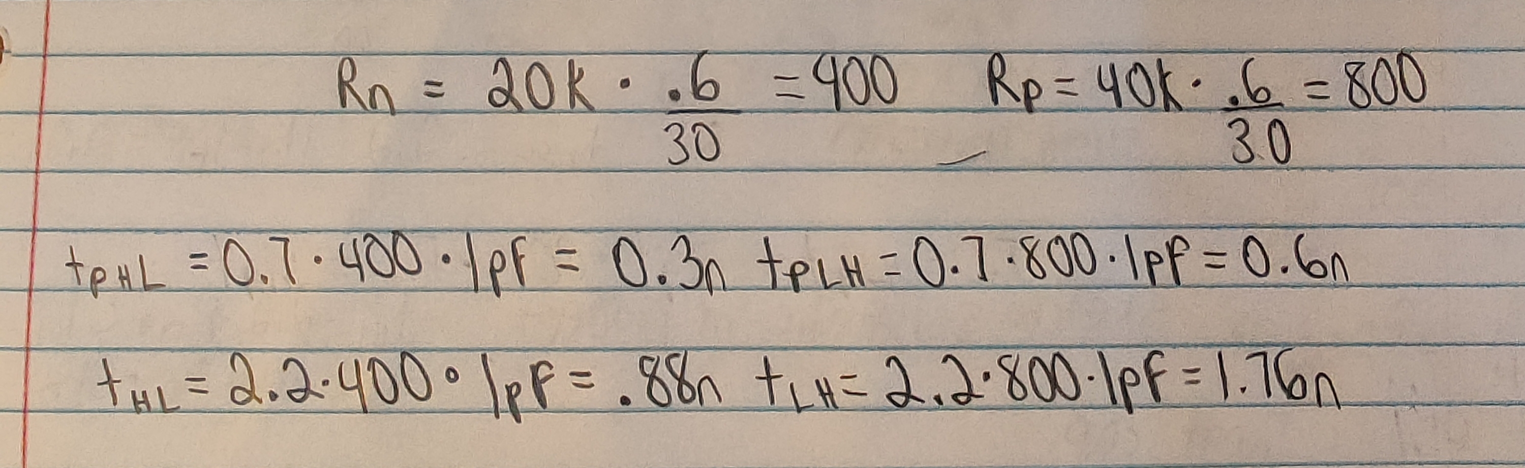
For
the top MOSFETs, I decided to go with 6u/0.6u for M1 as it is not as
important and also uses less layout area and power. For M2 and the
other MOSFETs, I decided to go with 30u/0.6u since larger sizes didn't
seem to change the results as much and would make the layout process a
bit easier.
Calculating the propagation delays and the rise
and fall times. The calculations gives values which are smaller than
the maximum 4ns transition time that is allowed which can be seen below.
Part l : Designing the schematics with simulations
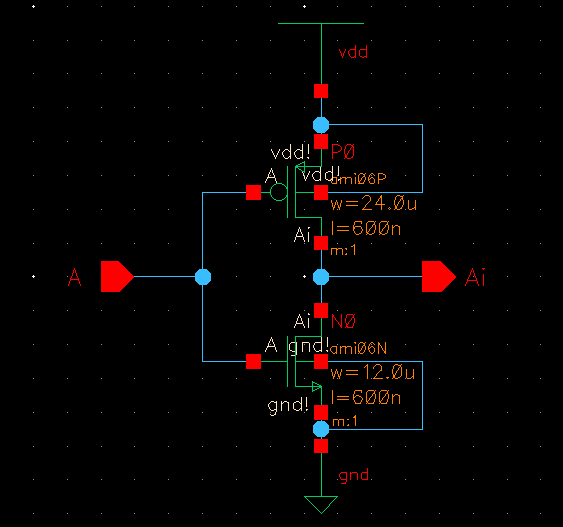
I first start off by making the schematic and symbol for the 24u/12u inverter that I will be using.
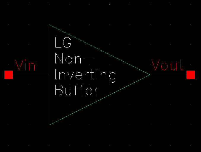
Schematic of the non inverting buffer
Symbol for the buffer
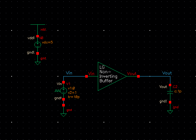
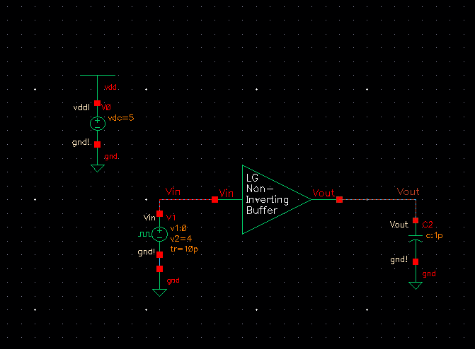
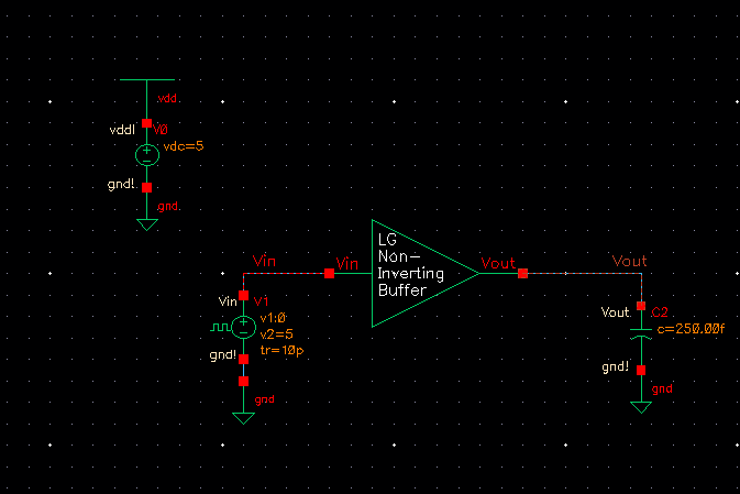
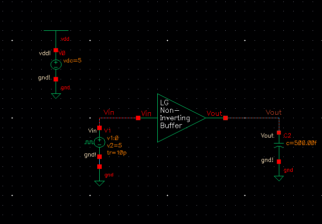
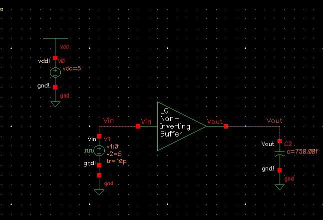
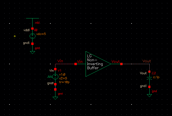
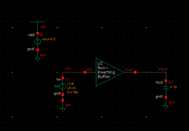
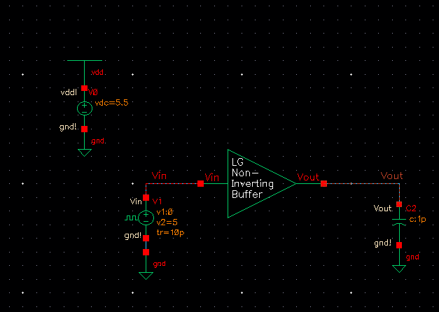
Setting up the schematic that I will use for simulations
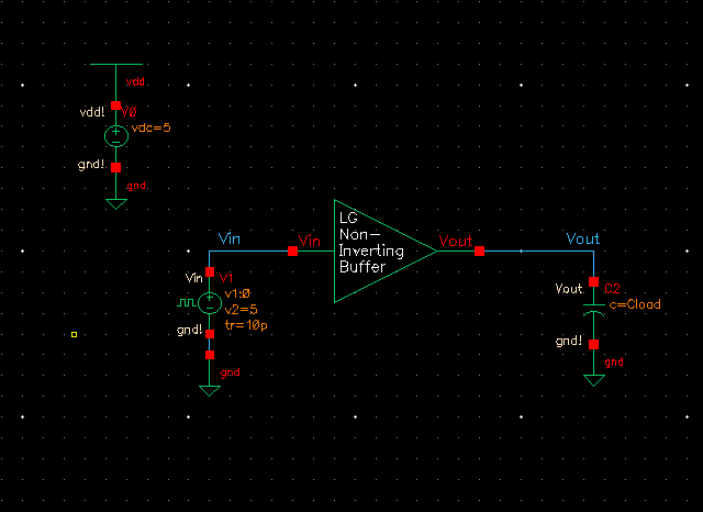
First, I will test the input logic where logic 0 is 1V or less and logic 1 is 3V or more.
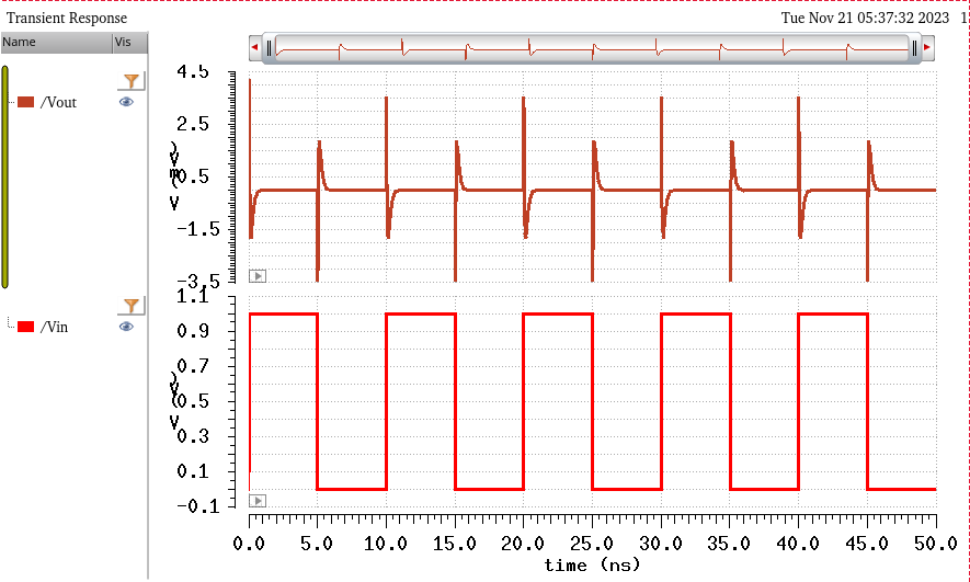
Vin = 1V
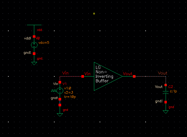
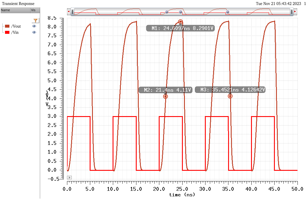
Vin = 3V
Vin = 4V
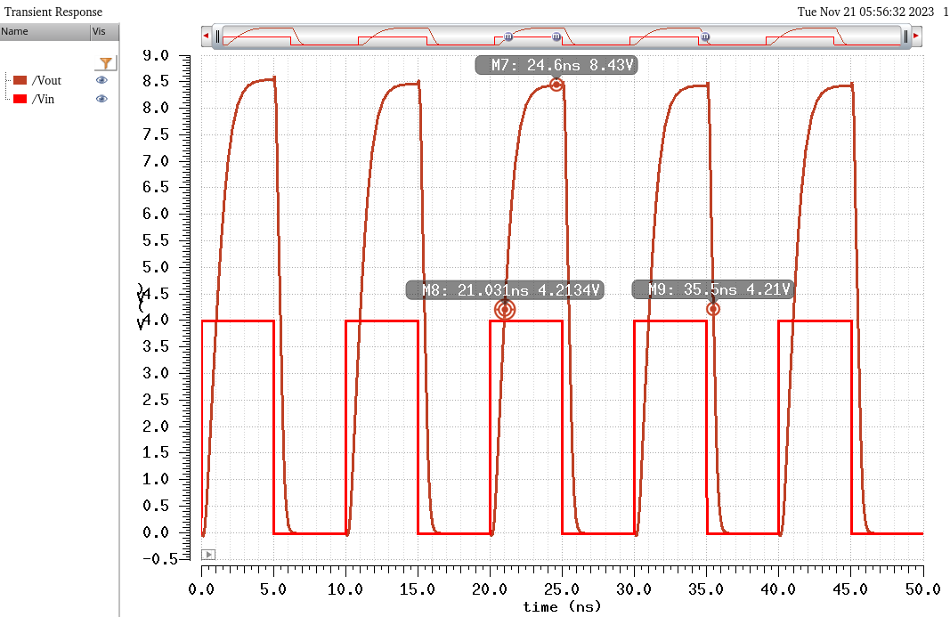
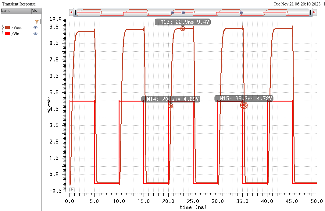
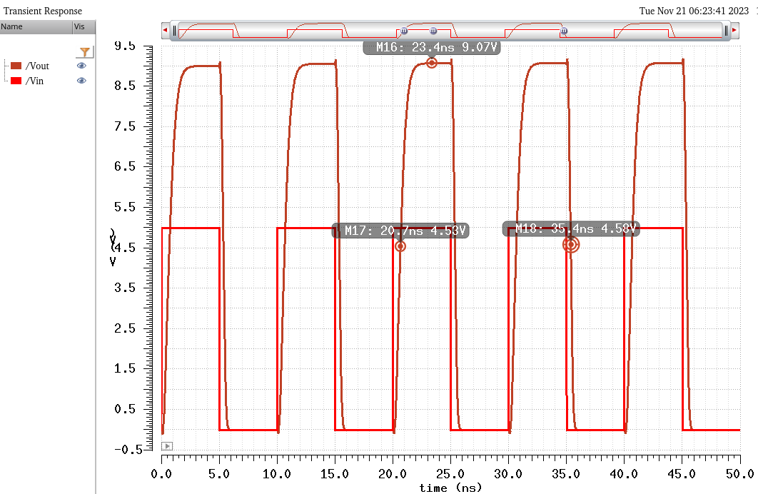
Now I will simulate using different loads varying from 0 to 1pF.
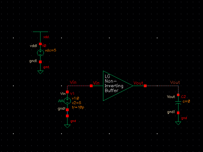
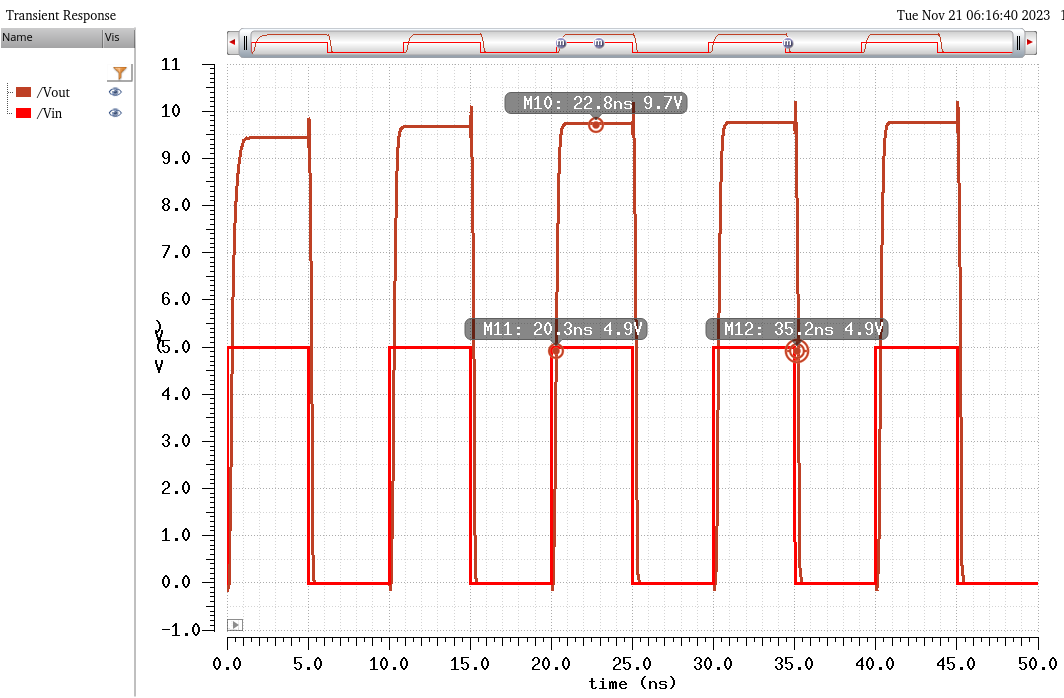
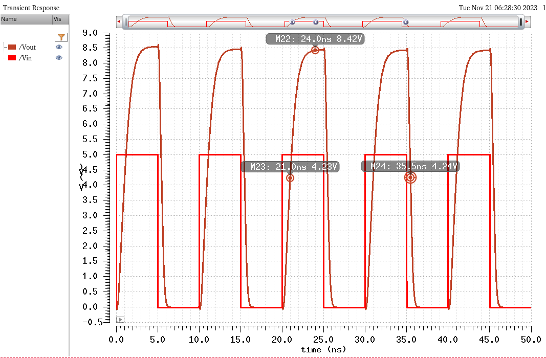
Load = 0p
Load = 0.25p
Load = 0.5p
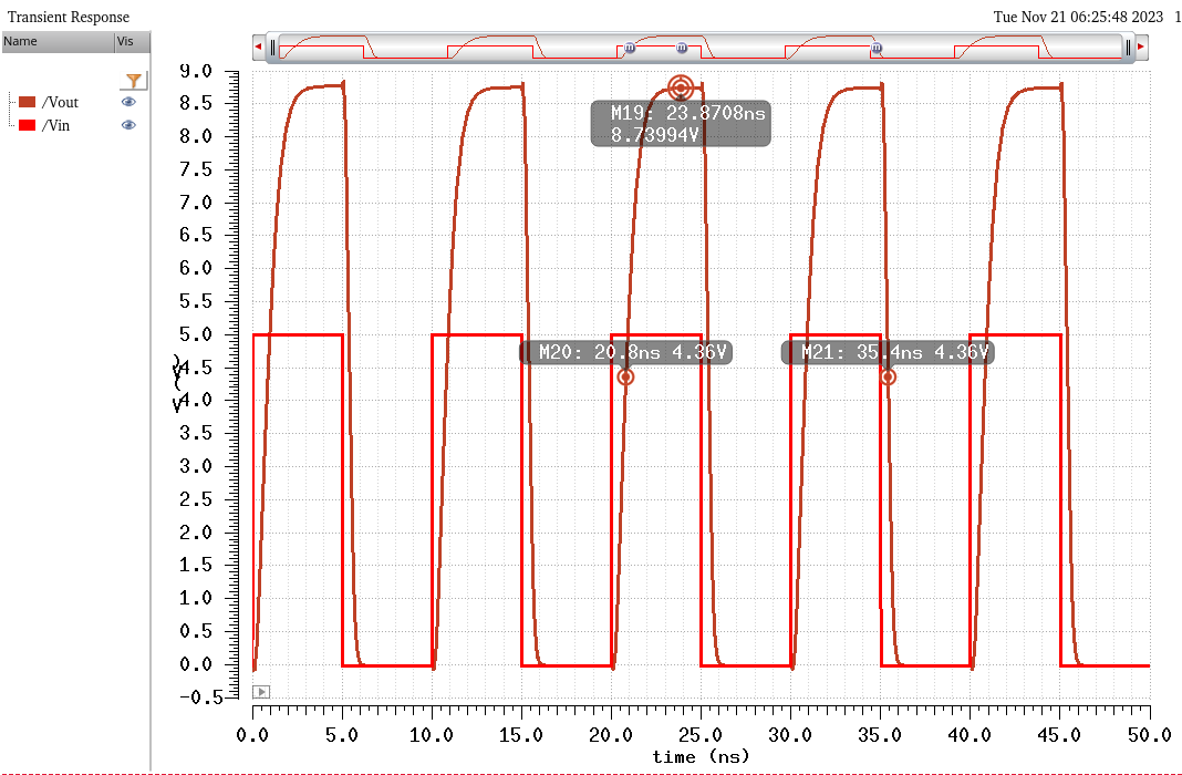
Load = 0.75p
Load = 1p
Now,
I will simulate with varying VDDs from 4.5 to 5.5. Since most of the
previous sims were done with VDD at 5V, I will only focus on 4.5 and
5.5.
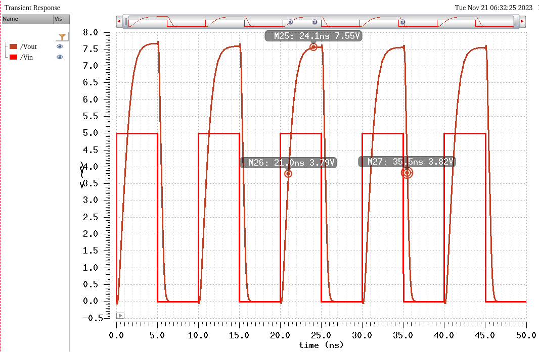
VDD = 4.5V
VDD = 5.5V
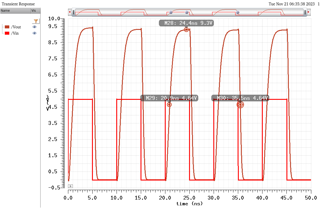
After
doing all of these simulations, we can see that they all fell into what
was required with output voltages greater than 7V for logic 1 which is
an input of 3V or greater and close to ground for logic 0 which is an
input of 1V or less. The desgin also still works when using varying
loads from 0 to 1pF and also when doing 4.5V to 5.5V for VDD. The
delays and transition times all fell relatively close to my hand
calculations which would make sense since the equations used for the
hand calculations give approximate values.
Part ll : Layout of the schematic
Layout
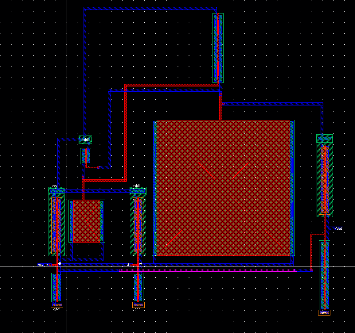
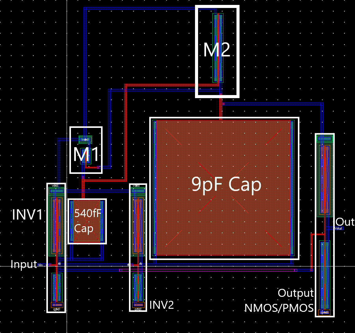
Layout with labels
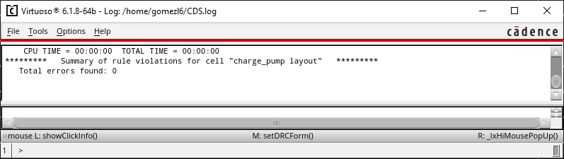
DRC Clean
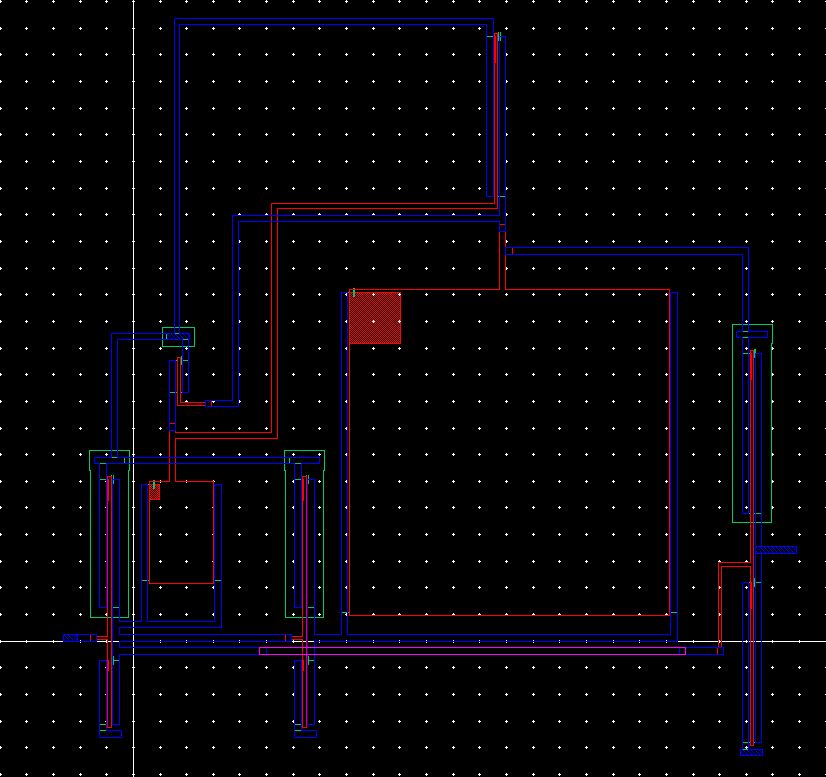
Extracted Layout
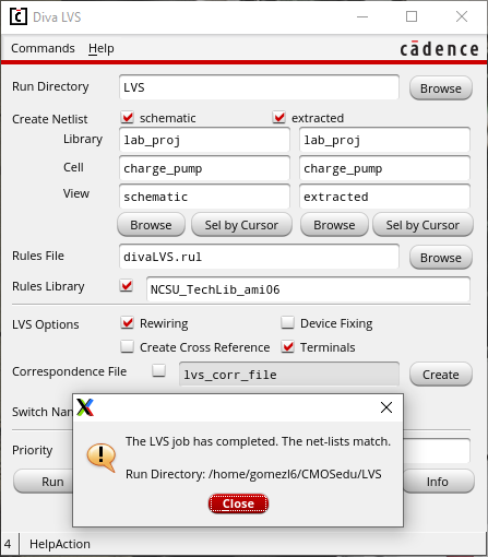
LVS Clean
This is the zip file of my project
proj_lg_f23.zip
Return to my Labs
Return to EE421L Labs