Lab 8 - ECE 421L
Authored
by: Jalen Solis (solisj8@unlv.nevada.edu), Martin Mercado (mercam13@unlv.nevada.edu), Larri Gomez (gomezl6@unlv.nevada.edu)
December 6, 2023
The purpose of this lab is to create a chip using circuits made in previous labs. The
first part of the lab requires all students to complete tutorial 6,
this tutorial teaches students how to layout a pad, padframe, and chip
within Cadence. Using what was learned from the tutorial, students will
form into groups of 3 to put test structures onto a chip. Each test
circuit will have its own power but the ground will be shared between
all circuits.
The following circuits will be put onto the chip and tested:
- Course projects
- A 31-stage ring oscillator
- NAND and NOR gates using 6u/0.6u NMOSs and PMOSs
- An inverter made with a 6u/0.6u NMOS and a 12u/0.6u PMOS
- Transistors, both PMOS and NMOS, measuring 6u/0.6u
- Using a 25k resistor and a 10k resistor to implement a voltage divider
- A 25k resistor implemented using the n-well
Prelab
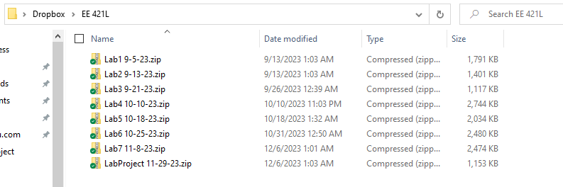
Before we start the prelab, it is important to back up all the work that was done in previous labs:
- Here we have every completed lab along with the project that is zipped up and kept in a Dropbox folder
- The
reason for the use of the Dropbox is to allow easy access on any device
in any location should something happen to the orginal files
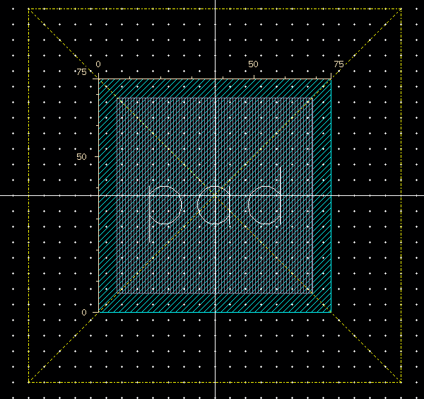
The first step in the prelab is to create the layout of a single pad:
- The dimensions of the single pad will be 75u/75u
- These pads will be used as input/output pins of the circuits
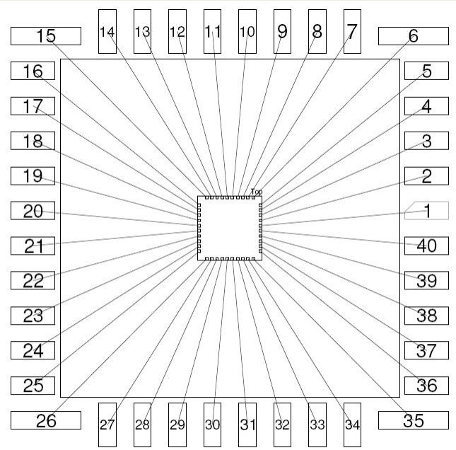
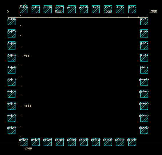
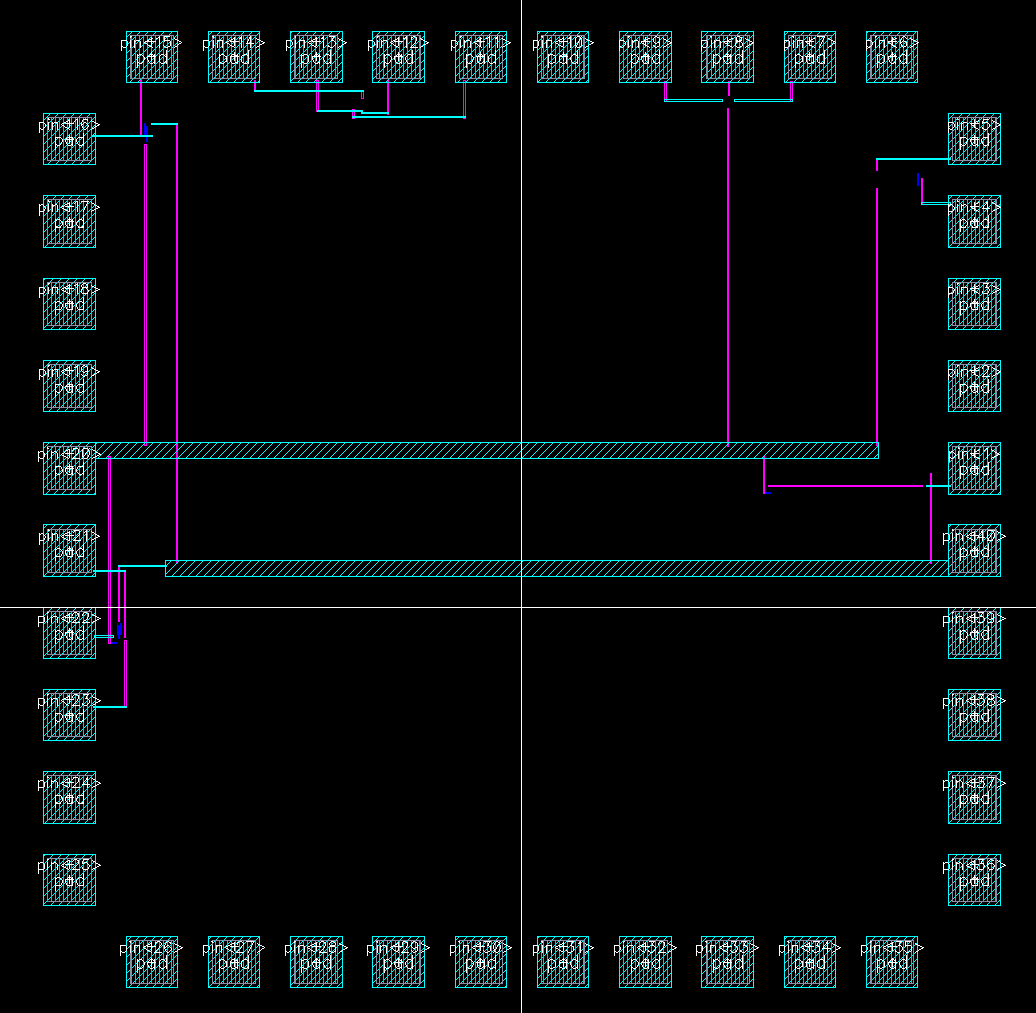
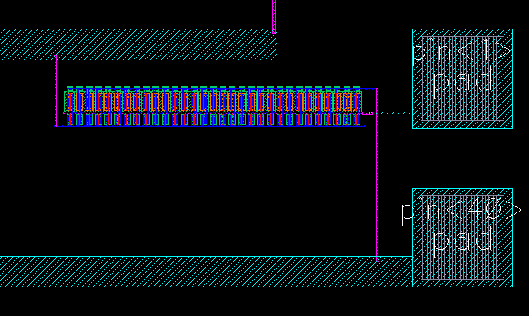
Once the single pad is created the next thing to do is to create a padframe that has a total of 40 pads
A new layout will be created called "padframe" and will need the single pad that was created previously:
- Two arrays are created to make a square that has 12 x 12 pads
- The middle can be deleted along with the corners
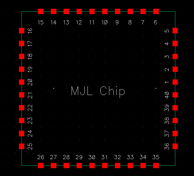
- The individual pads then need to be named according to the bonding diagram
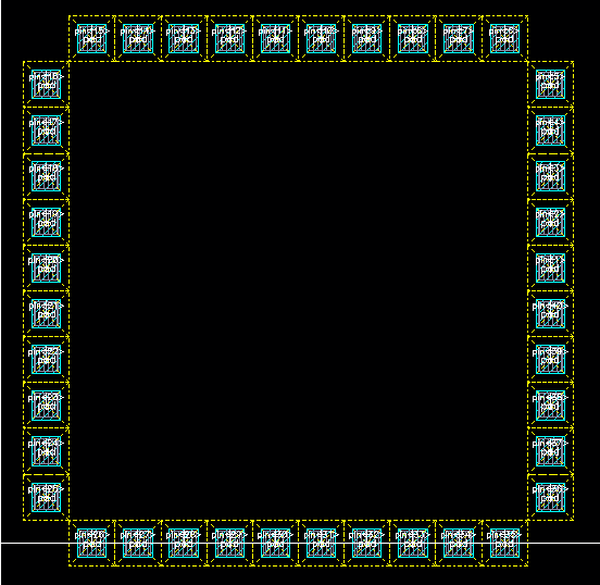
The pad layers can then be removed an the length and width of the chip can be measured:
Now that the chip has been created the next part is to create the schematics
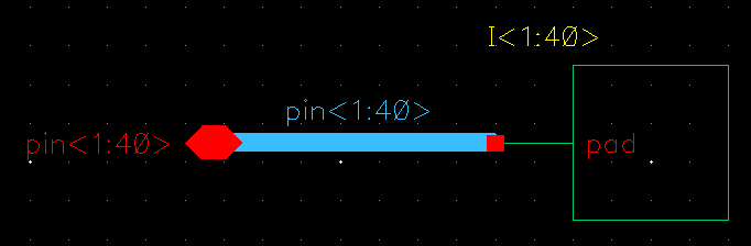
Pad:
- Schematic of single pad cell
- Symbol view of single pad cell

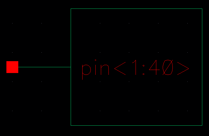
Pad Frame:
- Schematic of pad frame
- Symbol view of pad frame
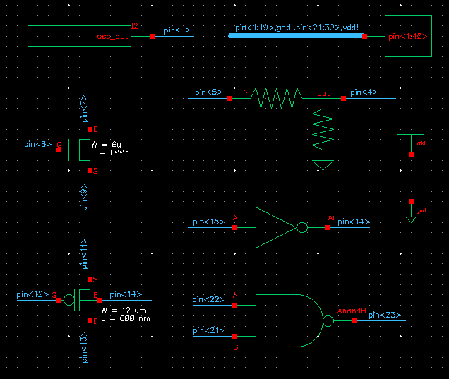
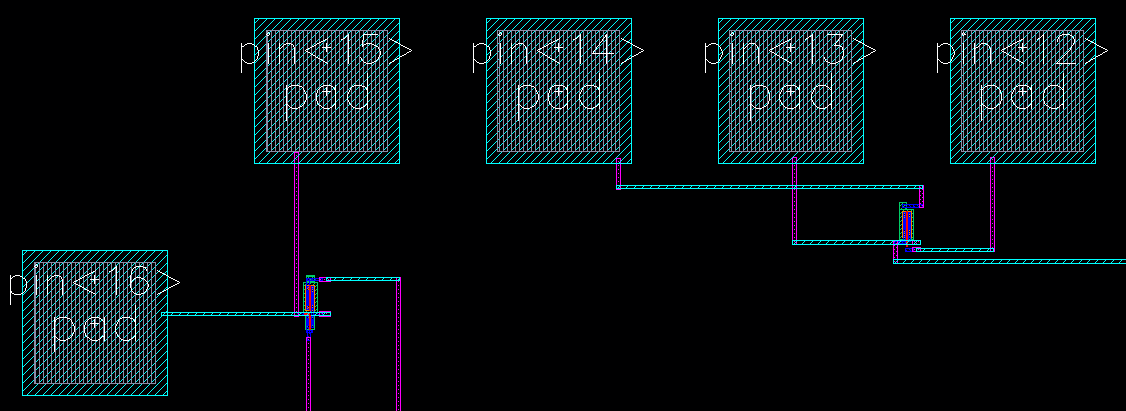
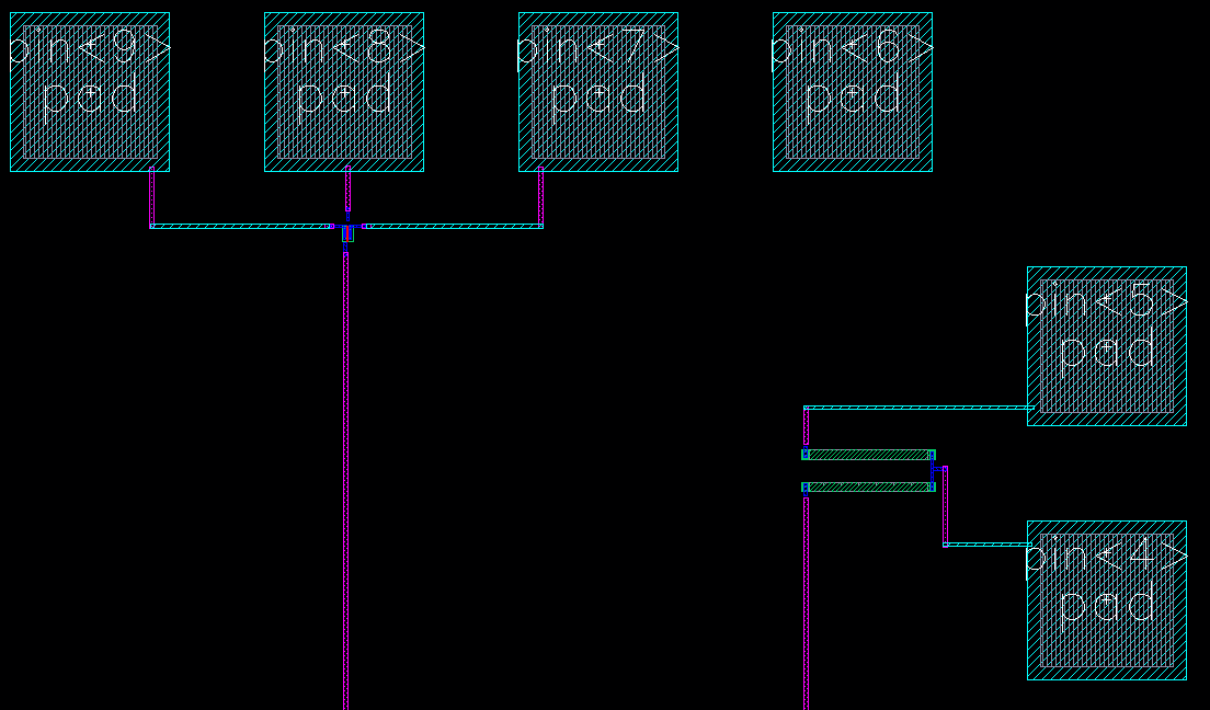
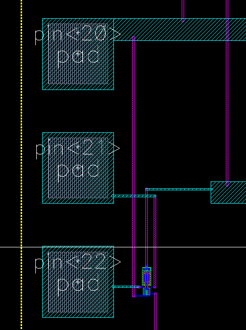
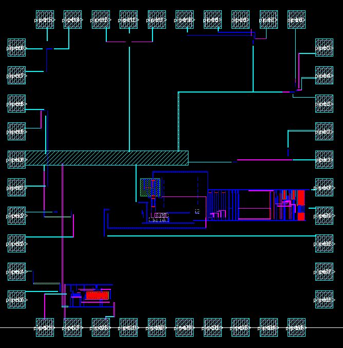
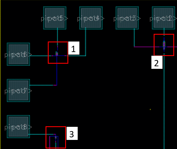
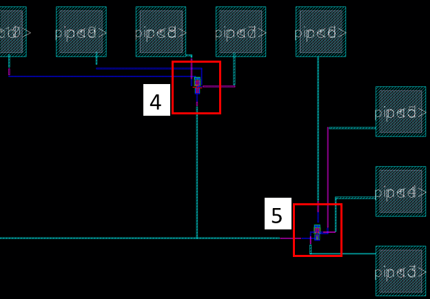
With the chip ready for layout we can use several circuits that were made from previous labs and implement them into the design:
- Each input/output will recieve a pin along with gnd and vdd
- The left over pins will be floating and the errors can be ignored
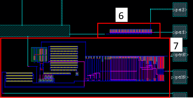
With the schematic completed for the chip the layout can be started:
Layout of Inverter and NMOS:
Layout of NMOS and Voltage Divider:
Layout of Ring Oscillator and common VDD pin:
Layout of NAND Gate and common GND pin:
The layout can then be saved and this concludes the prelab
Lab
Using
what was learned from the prelab we can create our own chip and place
several circuits that we've made including some projects.
The first thing to do is to place all the circuits that will be on the chip in a schematic:
- It
is important to note that all circuits that use the VDD symbol must be
replaced because we cannot have multiple circuits share a VDD
- To solve this problem each circuits power supply will be placed on a pad
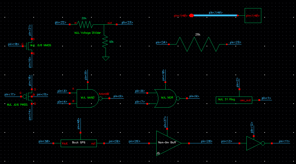
Once the schematic is created we can move on to the symbol of the chip:
- Pin 20 will be the common ground
Now that the symbol is completed out we can create the layout of the circuit:
- PMOS
- Inverter
- NMOS
4. NOR Gate
5. NAND Gate
6. Ring Oscillator
7. Synchronous SPS Buck Converter
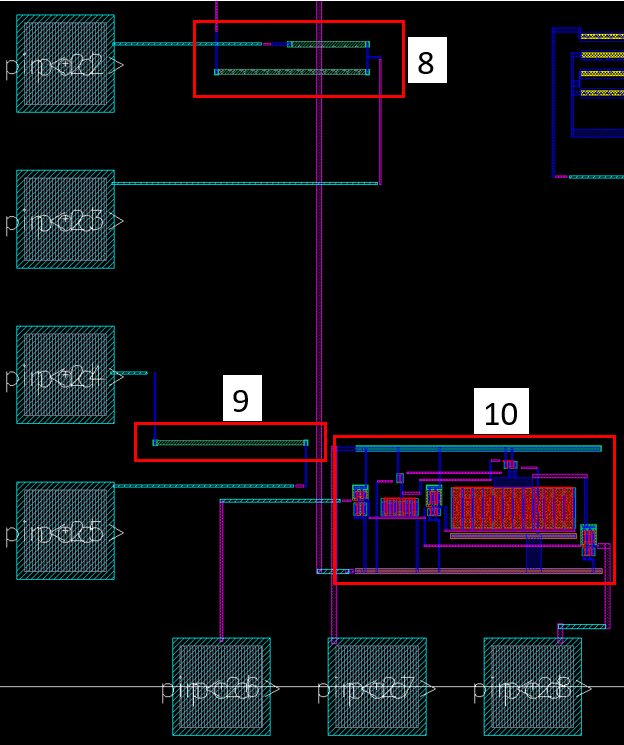
8. Voltage Divider
9. 25k N-Well Resistor
10. Non-Inverting Buffer
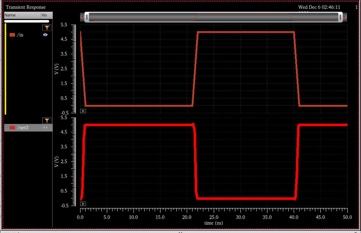
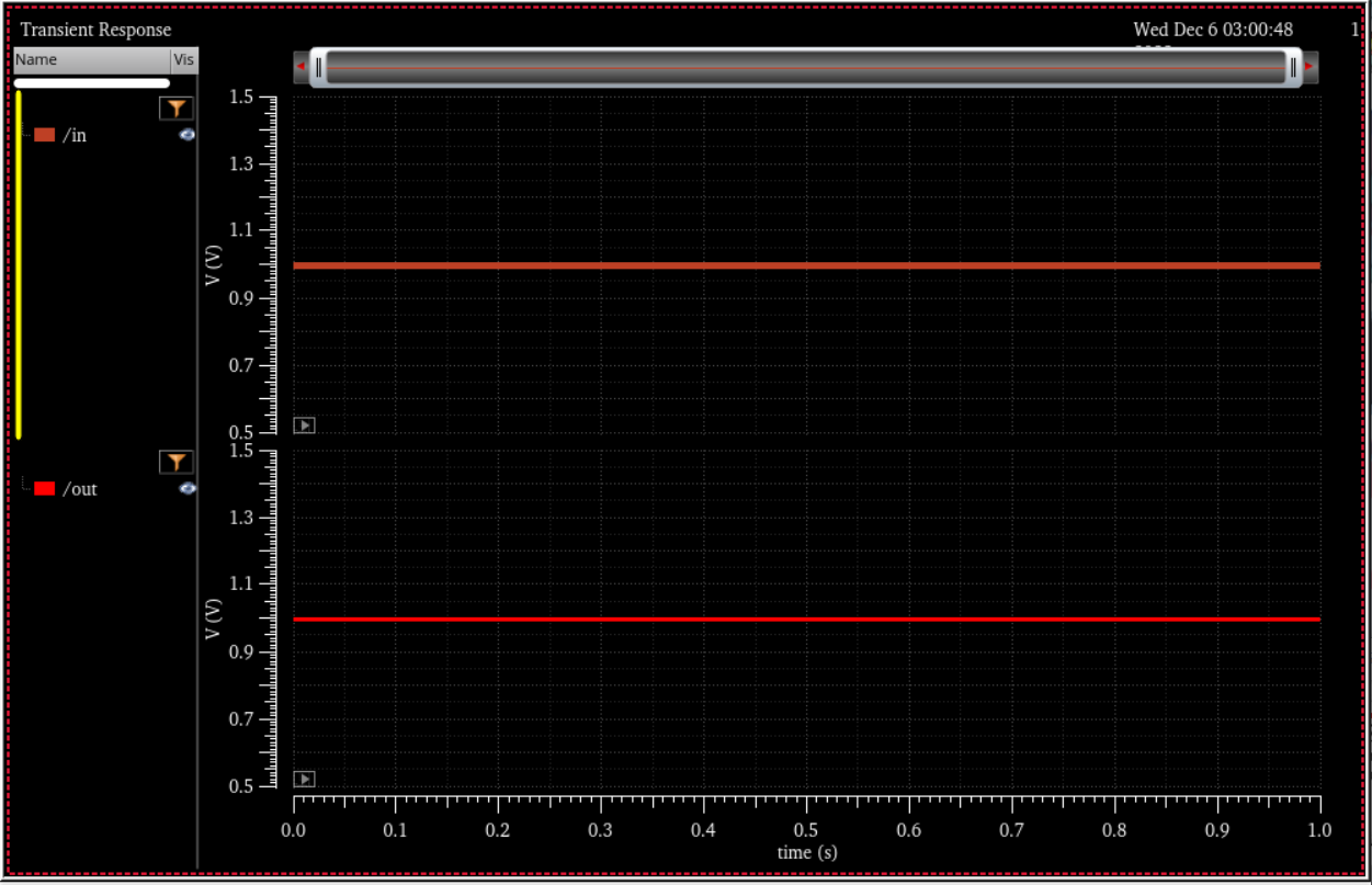
With our chip fully laid out, we can run some simulations on the chip to make sure it is functioning correctly:
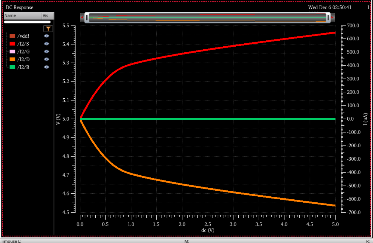
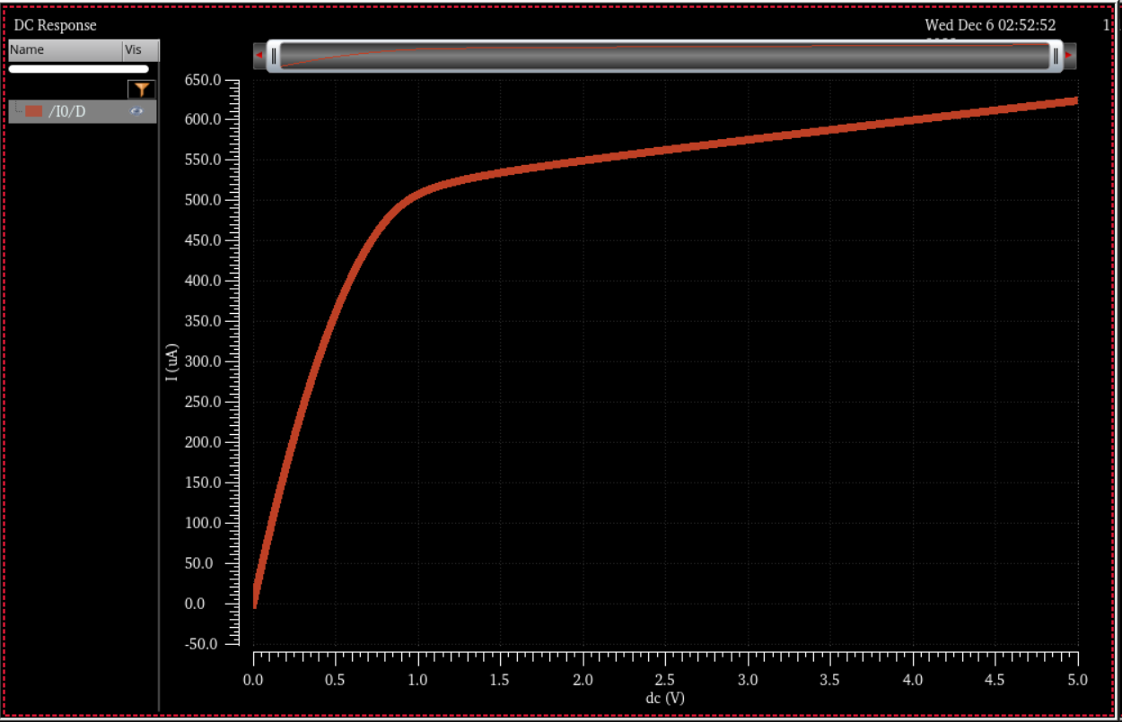
- In this example we will be showing how to test the Voltage Divider and Non-Inverting Buffer
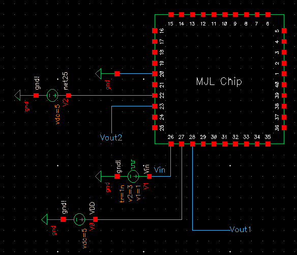
- Find out what pins are connected to the input, output and supply power of the circuit
- Place the power supply down and connect a wire to the pin associated with it
- Connect ground to pin 20
- Connect the input to the correct pin (Voltage Divider = pin 22, Non-Inverting Buffer = pin 26)
- Connect the output to the correct pin (Voltage Divider = pin 23, Non-Inverting Buffer = pin 28)
- Check & Save design (can ignore floating points or attach noConn)
- Open ADE L, select, and plot outputs
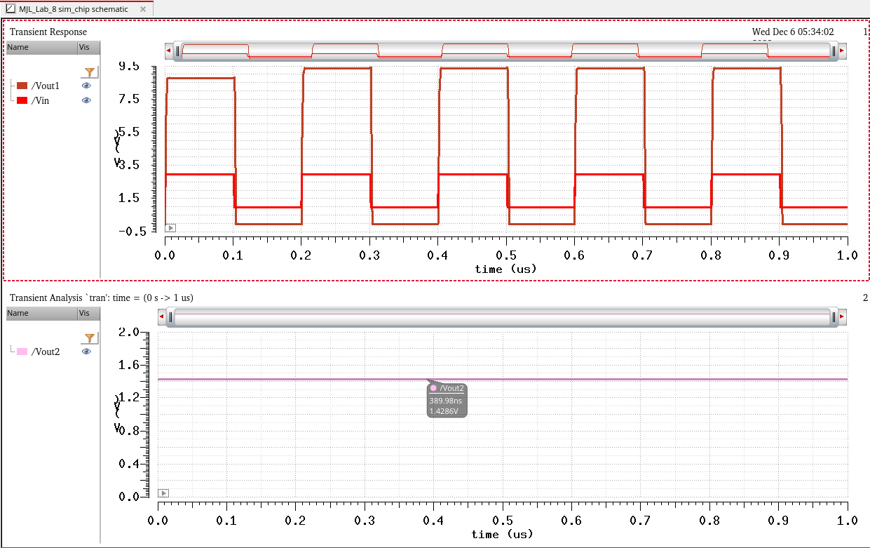
After running the simulations we see that our chip functions correctly
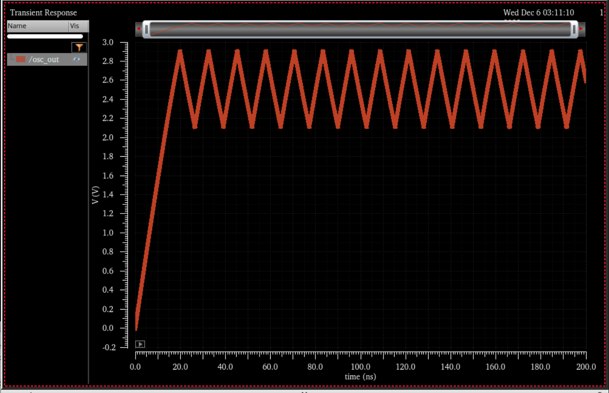
We can also run simulations of the other circuits to see if they work:
NOR:
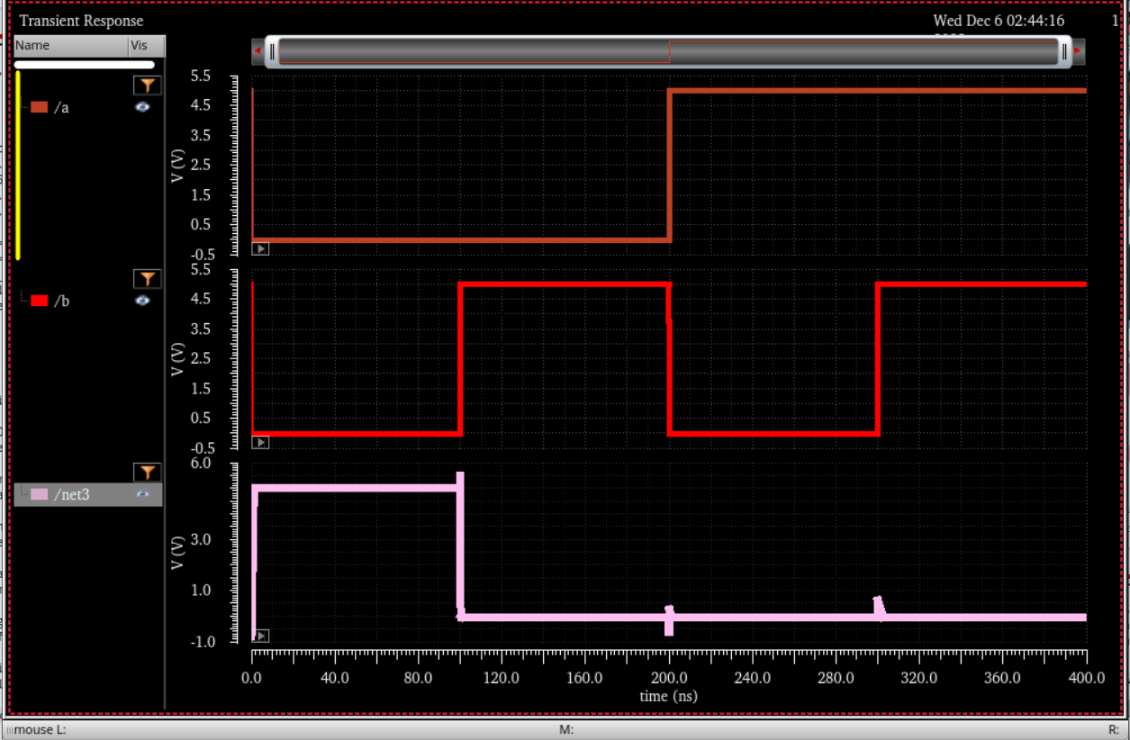
Inverter:
PMOS:
NMOS:
NAND:
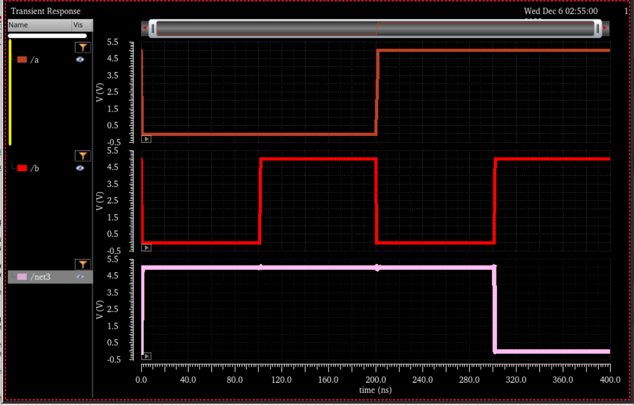
25k N-Well Resistor:
Ring Oscillator:
This concludes the lab
With the completion of lab 8 we can zip up our folder and back up our work:
Lab 8 File: Chip5_f23.zip
Return to EE 421L Labs