Lab 7 - EE 421L
Authored
by Larri Gomez, gomezl6@unlv.nevada.edu
10/25/23
Lab
description
In this lab, we practice working with buses and arrays by designing inverters, muxes, and high speed adders
Pre Lab
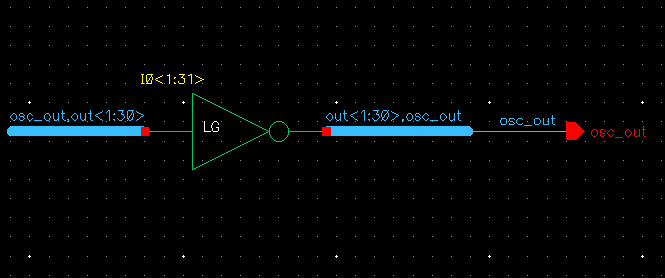
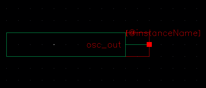
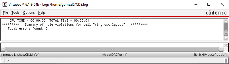
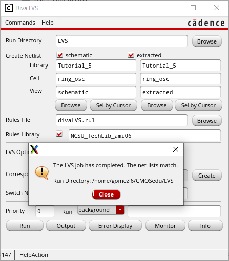
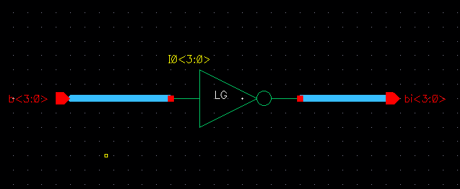
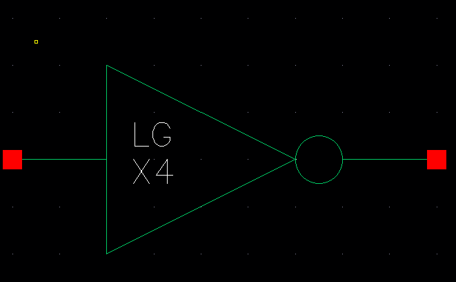
For the pre lab we are asked to go through Tutorial 5 which has us making a ring oscillator.
Schematic
Symbol
Layout
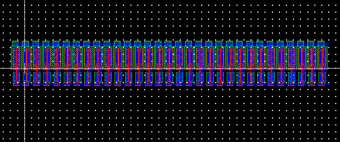
DRC clean/ LVS clean
Lab Work
4-bit inverter
schematic
symbol
sim schematic
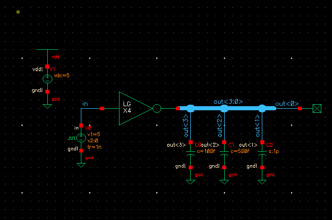
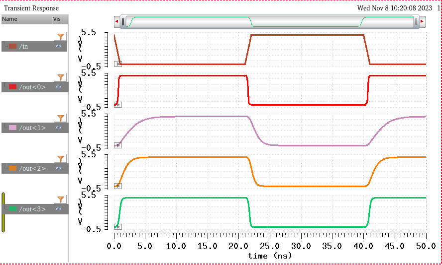
simulation
8-bit inverter
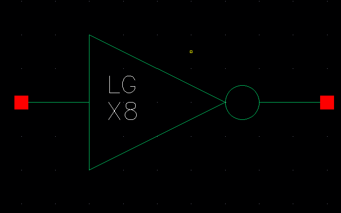
schematic
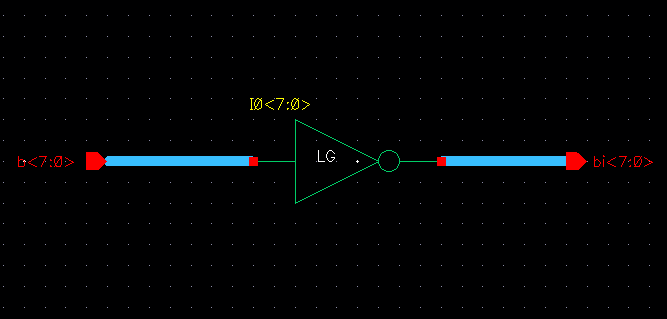
symbol
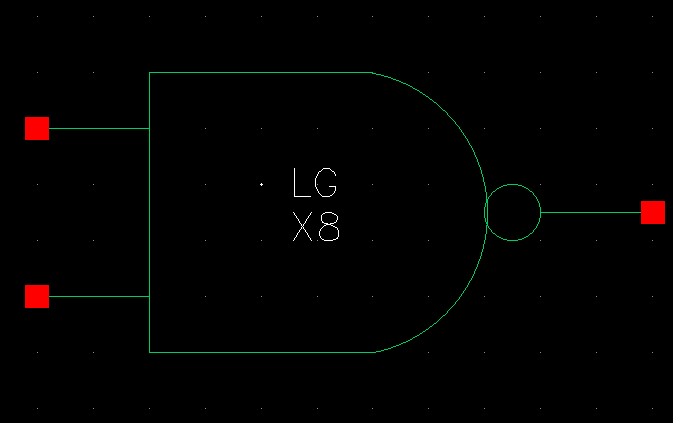
8-bit NAND gate
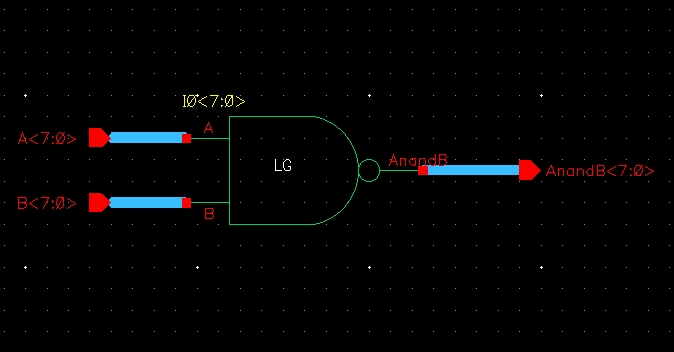
symbol
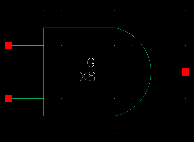
8-bit AND gate
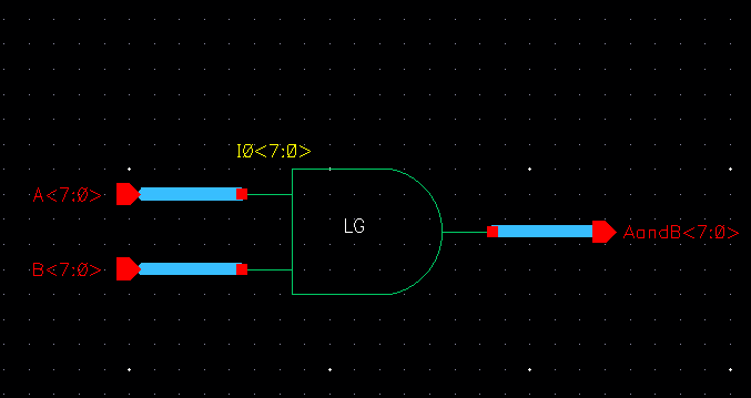
symbol
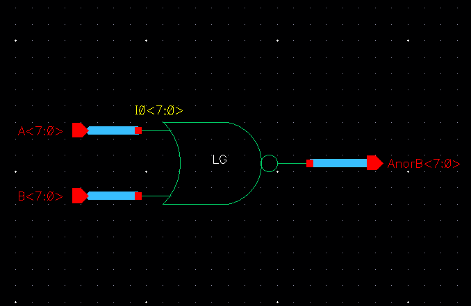
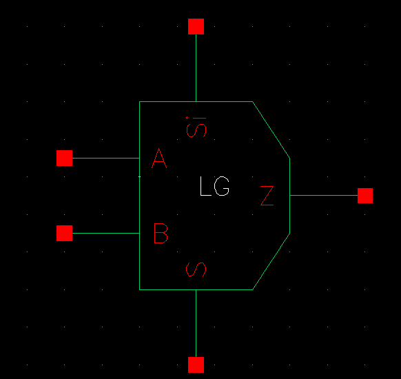
8-bit NOR gate
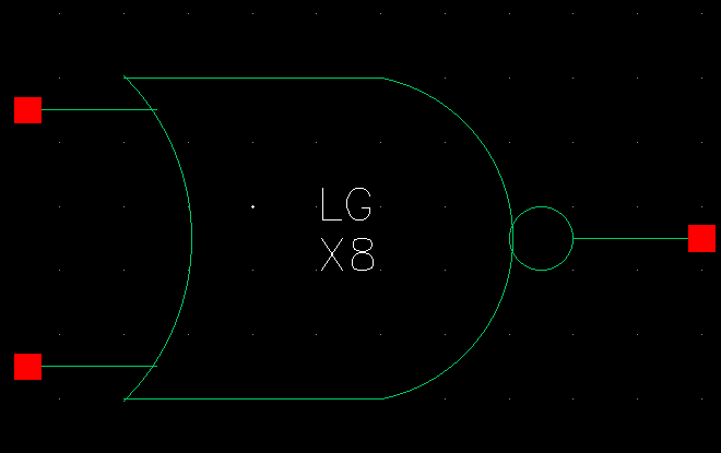
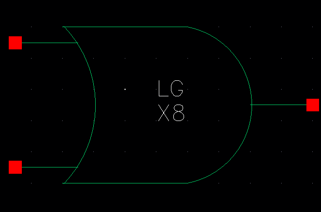
symbol
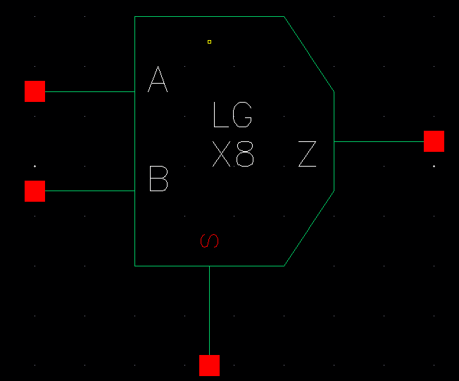
8-bit OR gate

symbol
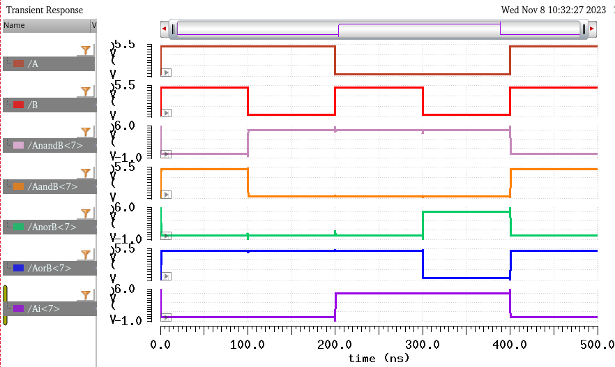
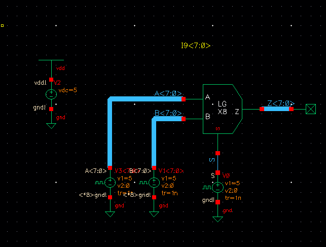
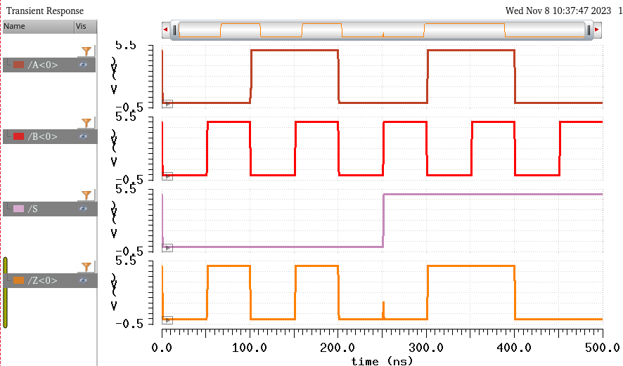
simulation of all gates together
2-to-1 MUX
8-bit 2-to-1 MUX/DEMUX schematic
symbol
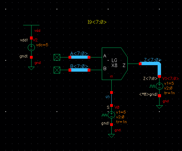
MUX sim schematic
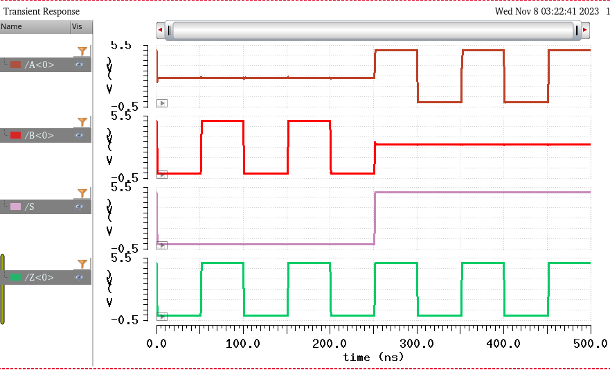
simulation
DEMUX sim schematic
simulation
Full Adder from Fig 12.20
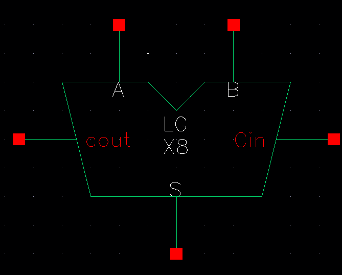
symbol
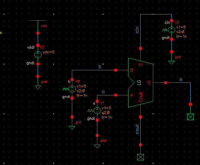
full adder sim setup
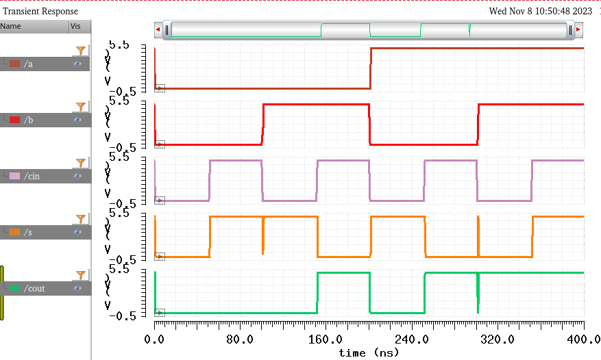
simulation
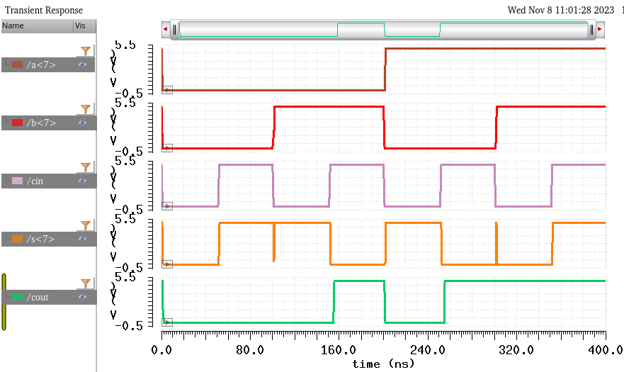
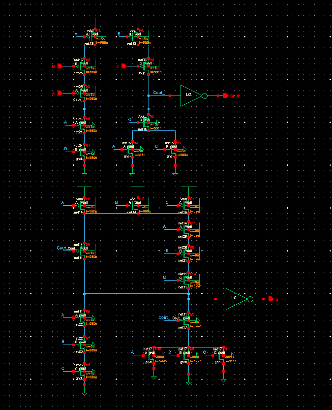
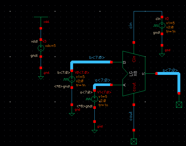
8-bit full adder schematic
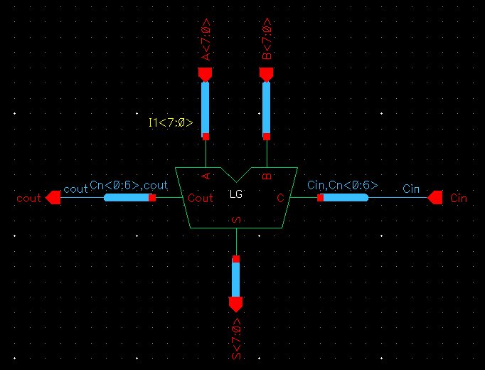
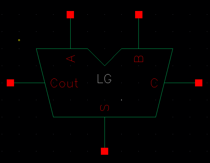
symbol
8-bit full adder sim schem
simulation