Lab 6 - EE 421L
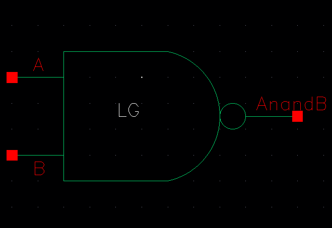
After checking for no errors, we can then create our symbol which should look like this.
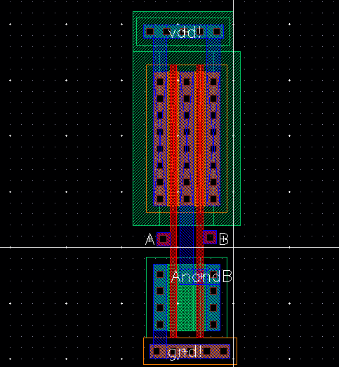
We can then proceed making our layout. The tutorial has us making to where the PMOS is 12u/0.6u which would not work because the PMOS in our schematic is 6u/0.6u. This is the 12u/0.6u.
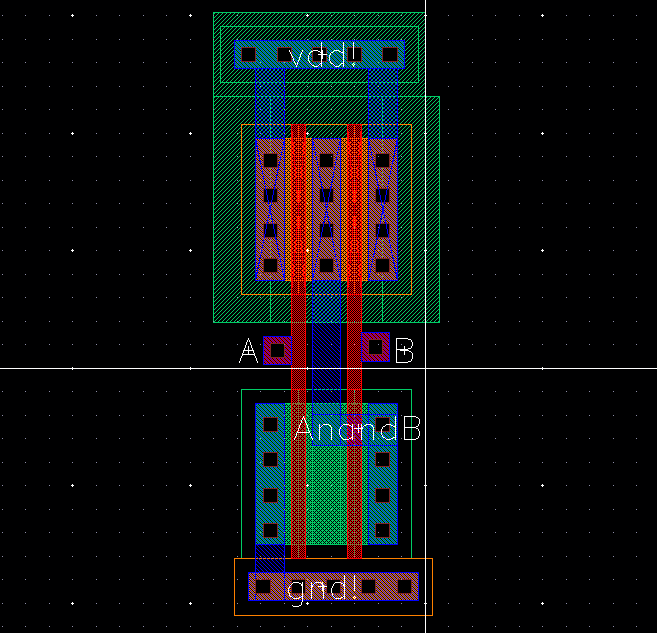
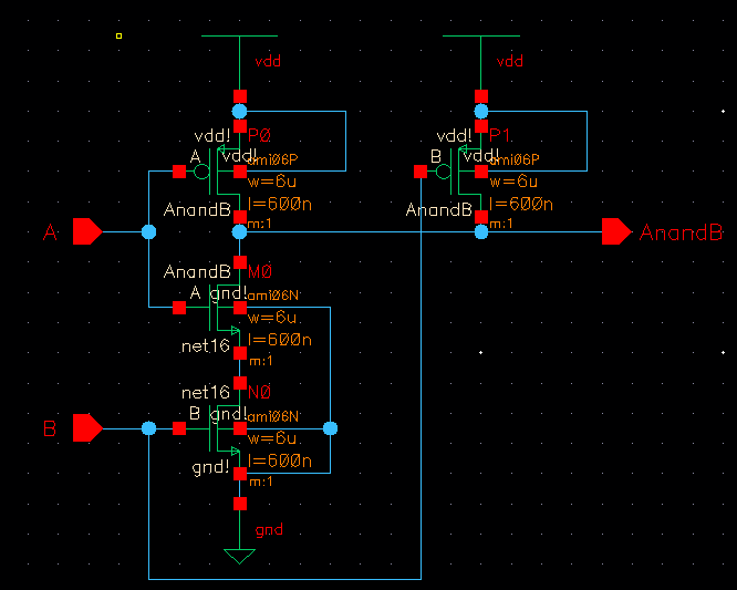
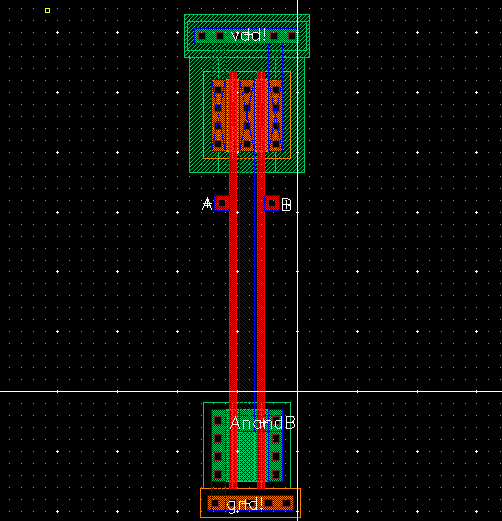
This is the layout with the PMOS at 6u/0.6u which is the correct one.
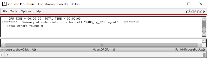
DRC clean
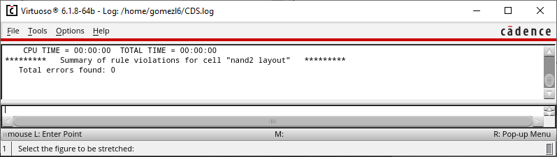
LVS clean

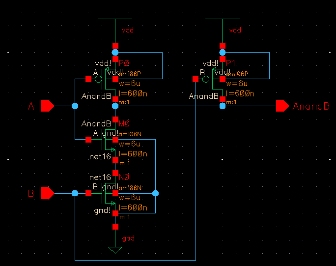
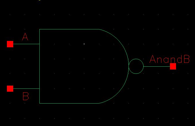
After checking for no errors, we can then create the corresponding symbol for the schematic which should look like this.
Now, we can go on to creating the layout for the gate which looks like this.
DRC clean
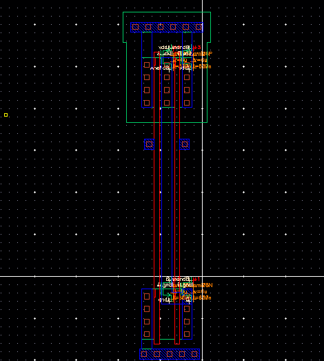
Extracted view of the layout that will be used for the LVS.
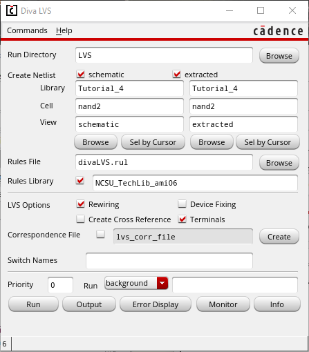
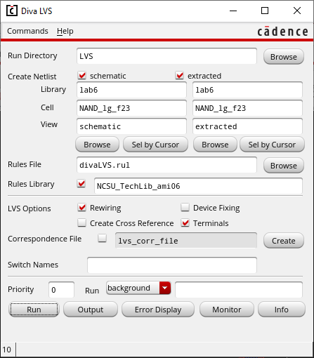
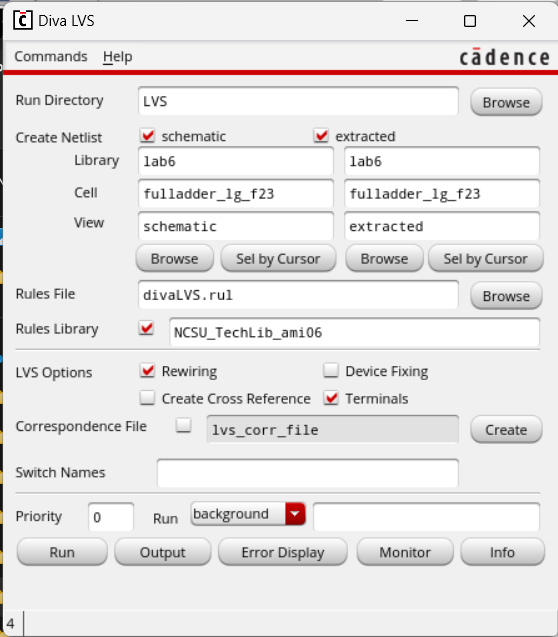
Setting up the LVS.
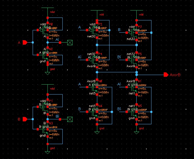
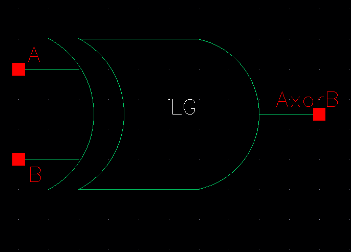
After checking for no errors, we can then create the XOR symbol.
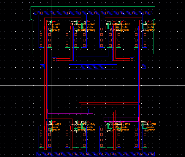
Now, we make the layout for the XOR gate.
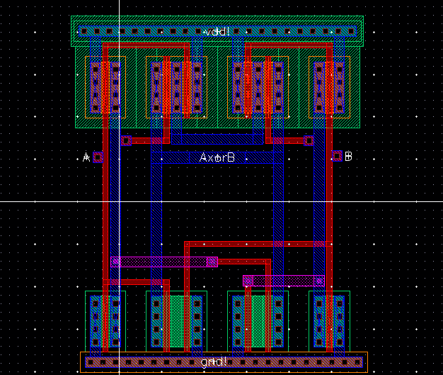
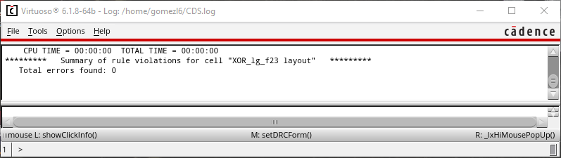
DRC clean
Extracted view that will be used for the LVS.
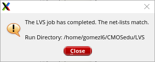
LVS clean


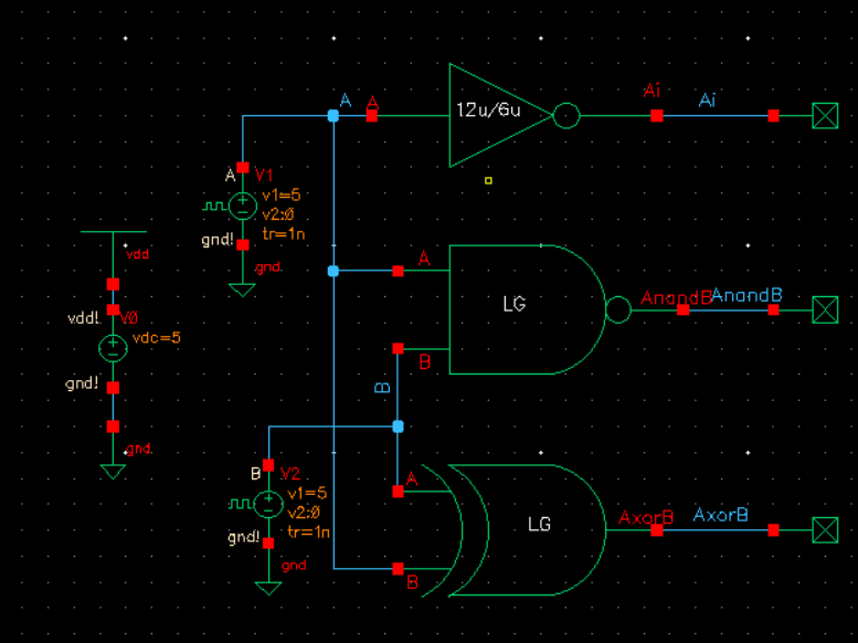
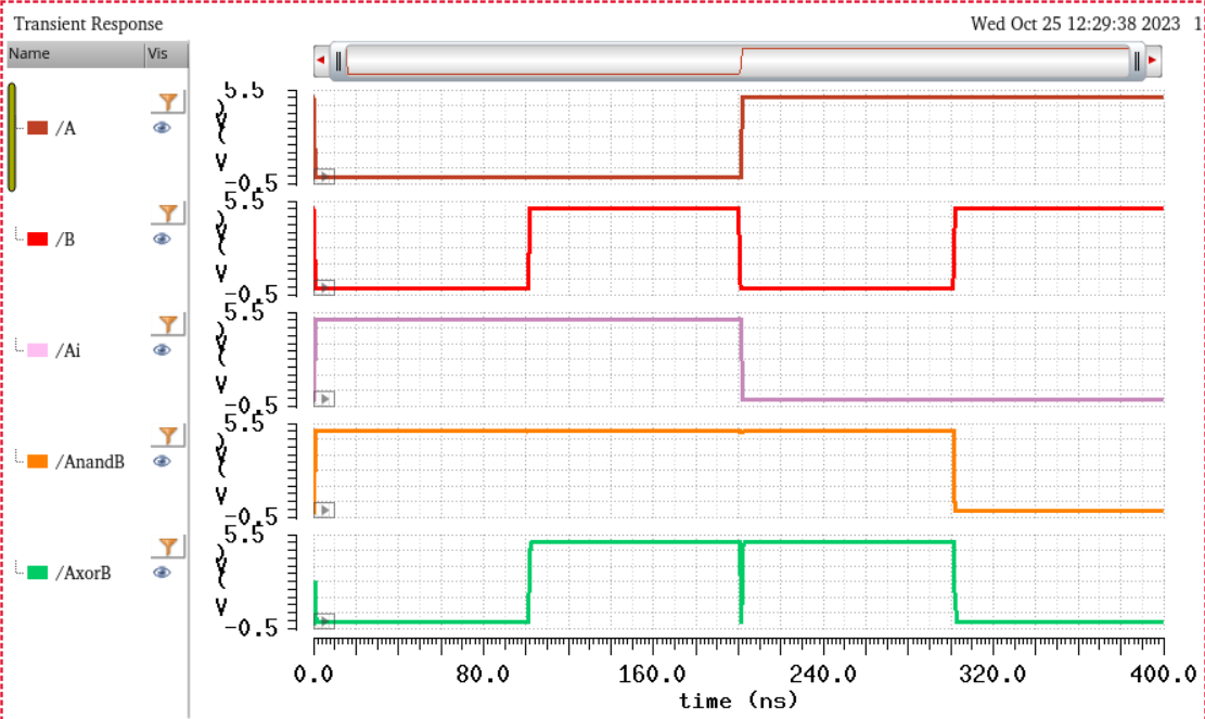
Now we can simulate it and this is what I got which gives the outputs for the 4 inputs for the NAND and XOR. It also seems that the output is coming out slightly glitchy which could be because of delays in the input which is not allowing to instantly get the next output.
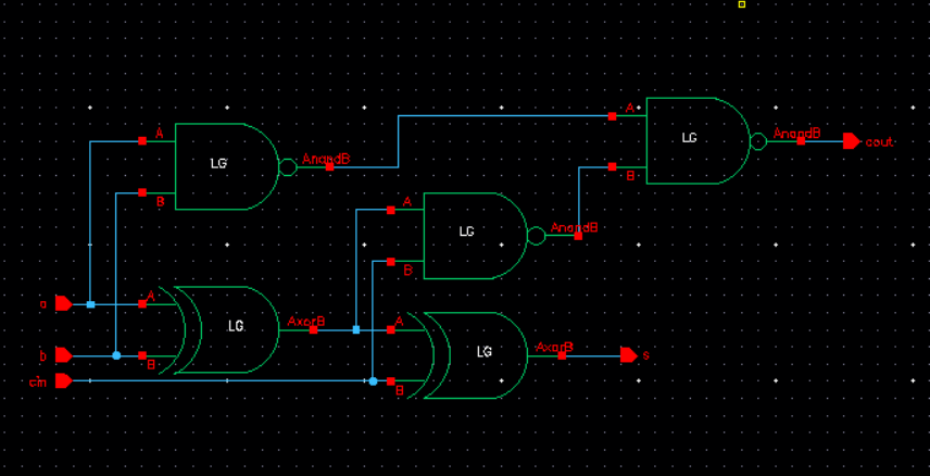
Lastly, we have to design a Full Adder which we can start by making the schematic.
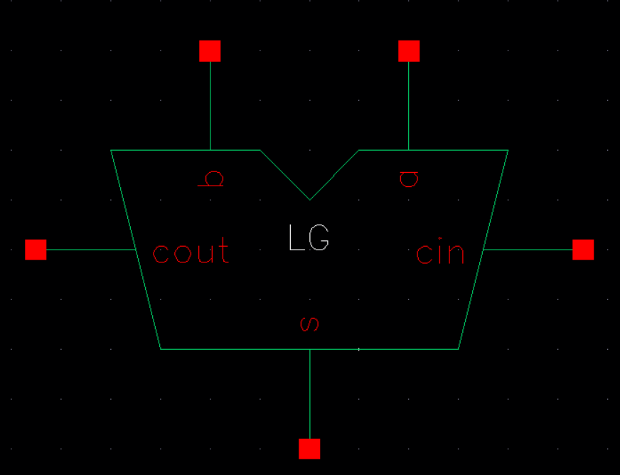
After checking for errors, we can then make the symbol for the Full Adder.
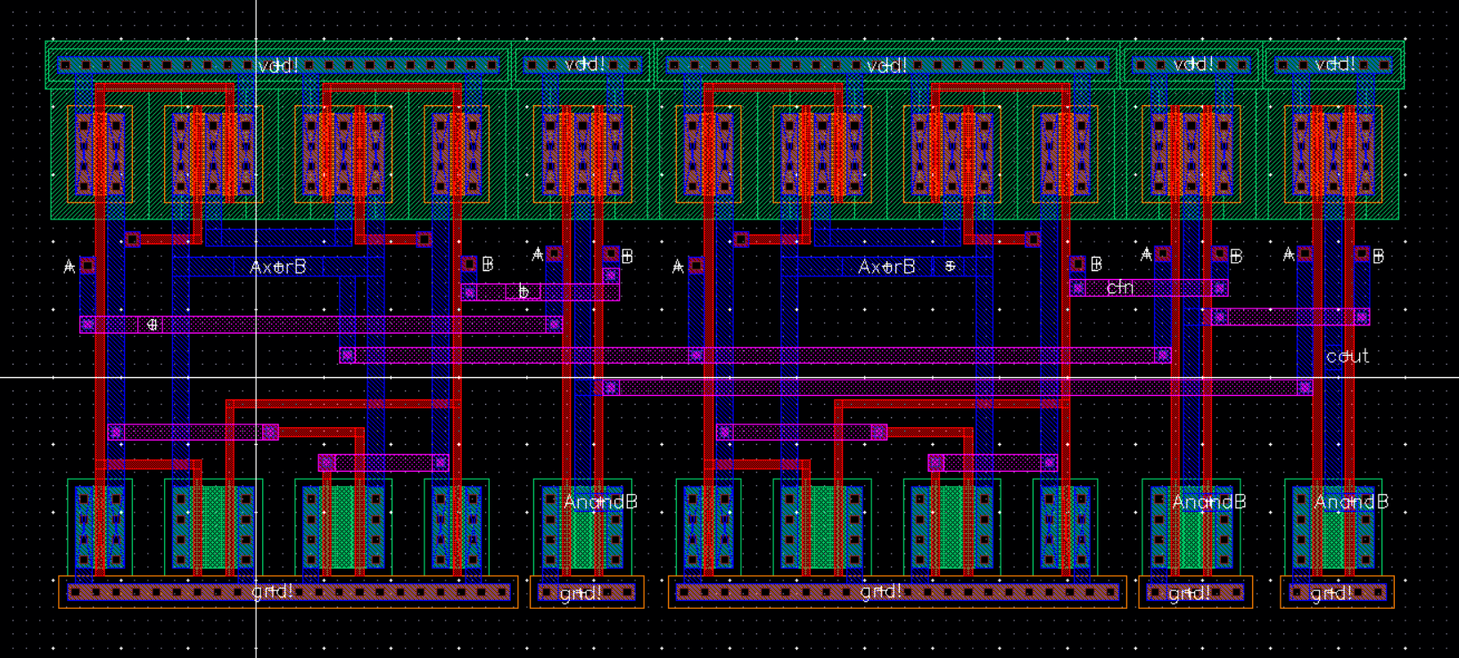
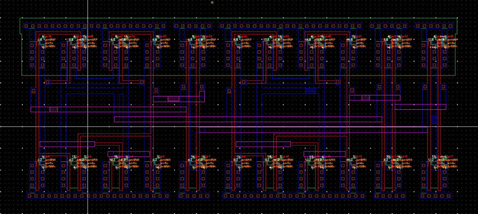
Now we can make the layout for the Full Adder which I make use of the layouts I already have for the NAND and the XOR and then make the connections for the new inputs and outputs.
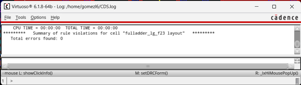
DRC clean
This is the extracted view that will be used for the LVS.
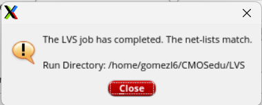
LVS clean
Now to make a schematic with the Full Adder symbol to simulate.
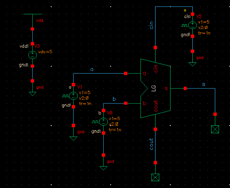
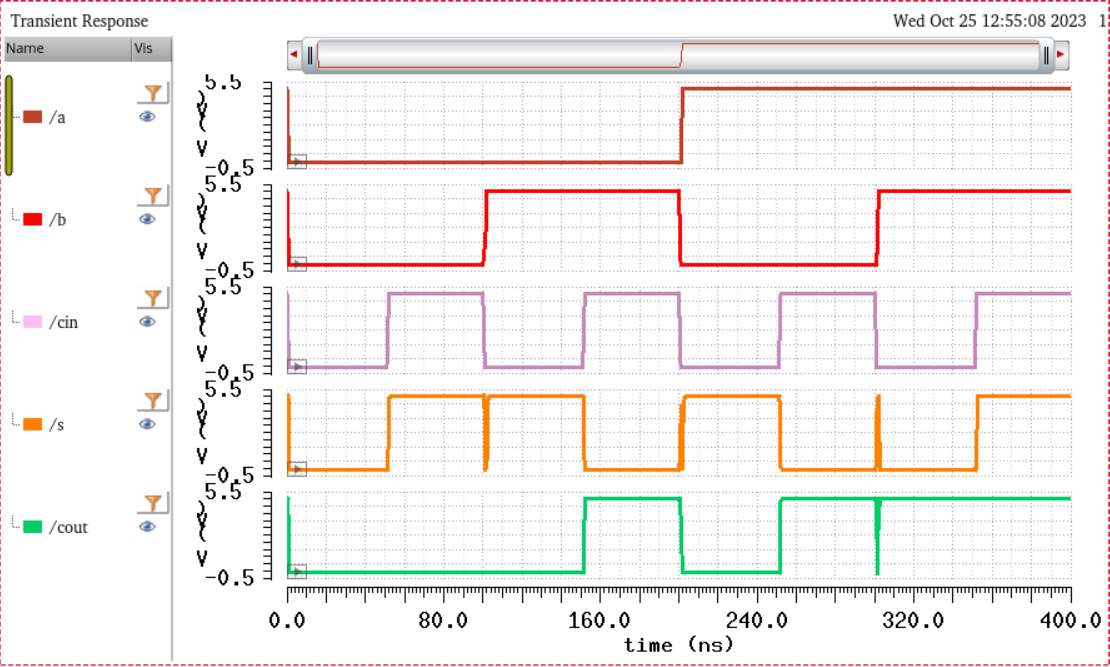
This is what I got for my simulation which matches up perfectly with the table.
This is the zip file containing my work for this lab lab6_lg.zip