Lab 5 - EE 421L 

Authored by Larri Gomez, gomezl6@unlv.nevada.edu

September 27, 2023


Lab description

 In this lab, we practice designing a CMOS inverter by creating a layout and a schematic of the invertor and then simulating the inverter with different sized capacitors.

Pre Lab 

For the pre lab, we are asked to go through Tutorial 3 which covers how to layout and simulate an inverter.

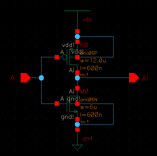
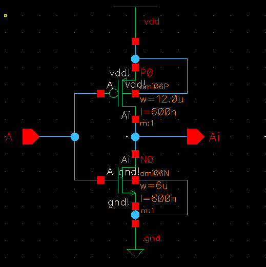
It first starts us off with creating a schematic for the invertor which can be seen below.

https://cmosedu.com/jbaker/courses/ee421L/f23/students/gomezl6/lab5/Pictures/pre1.png

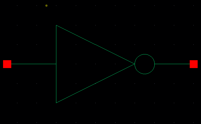
We then make a symbol out the schematic that we created and make it like how it is below. 

https://cmosedu.com/jbaker/courses/ee421L/f23/students/gomezl6/lab5/Pictures/pre2.png

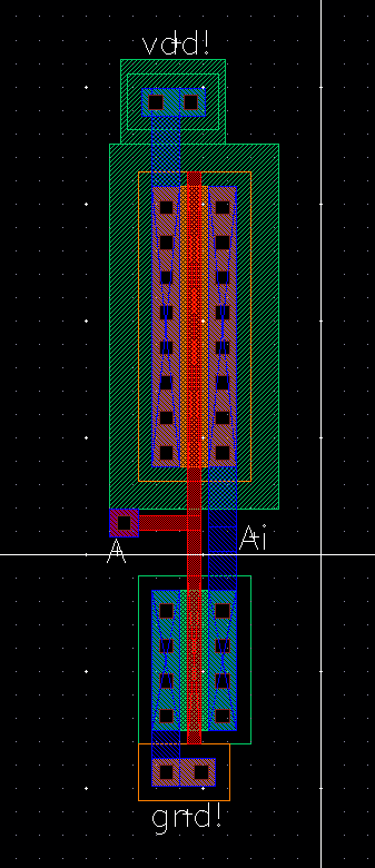
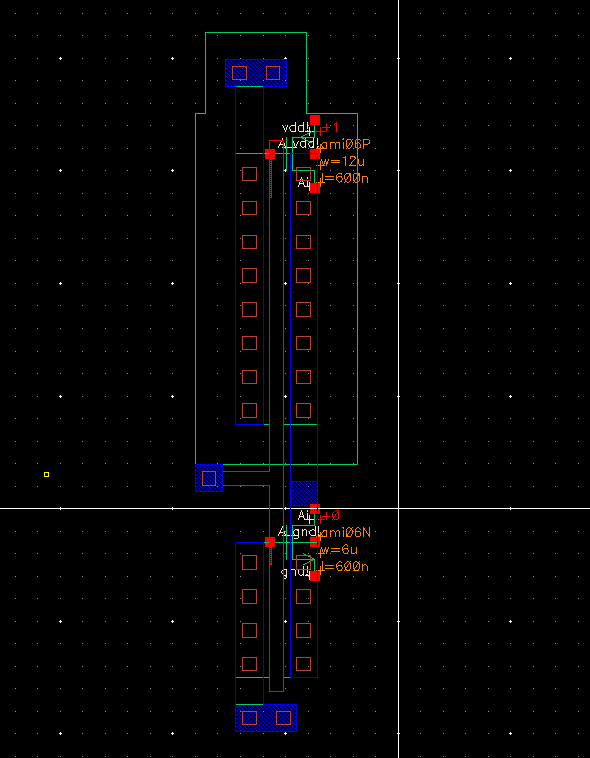
Now we make the layout for the inverter which should look like this. 

https://cmosedu.com/jbaker/courses/ee421L/f23/students/gomezl6/lab5/Pictures/pre3.png

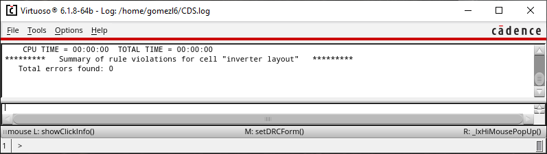
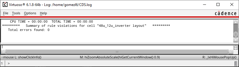
Now we check that it passes DRC.

https://cmosedu.com/jbaker/courses/ee421L/f23/students/gomezl6/lab5/Pictures/pre4.png

We can then extract the layout which will look like this 

https://cmosedu.com/jbaker/courses/ee421L/f23/students/gomezl6/lab5/Pictures/pre5.png

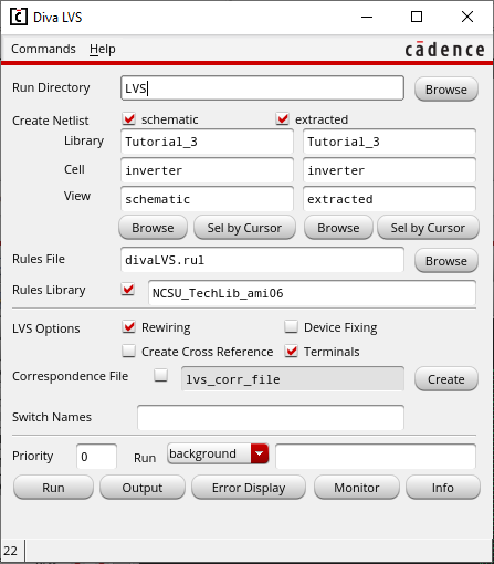
Now we are able to run the LVS using our schematic and our extracted layout

https://cmosedu.com/jbaker/courses/ee421L/f23/students/gomezl6/lab5/Pictures/pre6.png

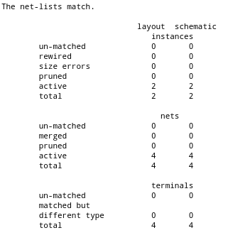
The LVS gives a match.

https://cmosedu.com/jbaker/courses/ee421L/f23/students/gomezl6/lab5/Pictures/pre7.png

https://cmosedu.com/jbaker/courses/ee421L/f23/students/gomezl6/lab5/Pictures/pre8.png

Lab Work 

For the lab, we are asked to make schematics, layouts, and symbols of two inverters with one being 12u/6u and the other being 48u/24u using a multiplier of 4. We are then also supposed to simulate the inverters using the symbols we createdby using the spectre and the UltraSim simulators.

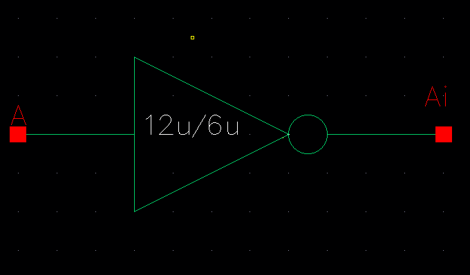
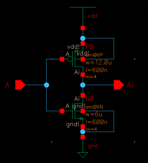
First, I will start off with the 12u/6u inverter by creating the schematic. 

https://cmosedu.com/jbaker/courses/ee421L/f23/students/gomezl6/lab5/Pictures/1.png

After checking for no errors, now we will create a symbol for the schematic 

https://cmosedu.com/jbaker/courses/ee421L/f23/students/gomezl6/lab5/Pictures/2.png

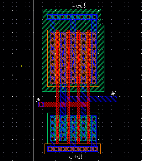
Now we make the corresponding layout for the inverter
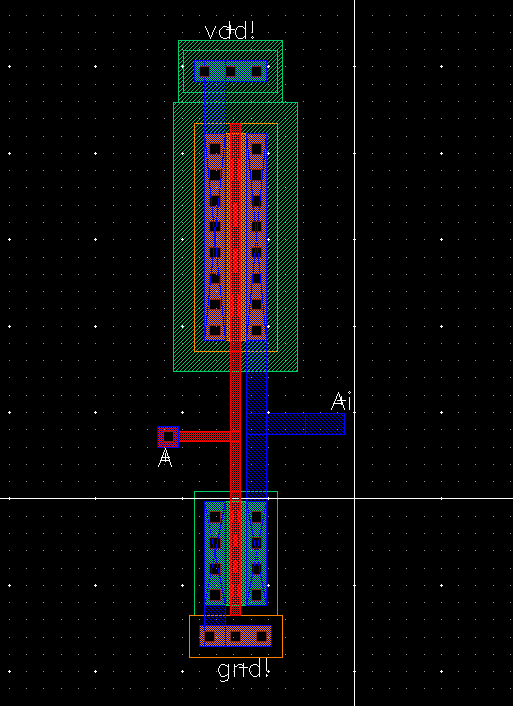
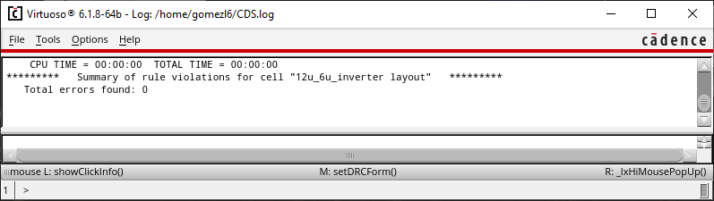
https://cmosedu.com/jbaker/courses/ee421L/f23/students/gomezl6/lab5/Pictures/3.png

DRC clean

https://cmosedu.com/jbaker/courses/ee421L/f23/students/gomezl6/lab5/Pictures/4.png

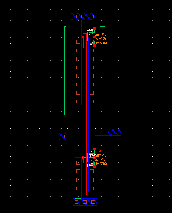
Now we extract the layout so that we can LVS.

https://cmosedu.com/jbaker/courses/ee421L/f23/students/gomezl6/lab5/Pictures/5.png 

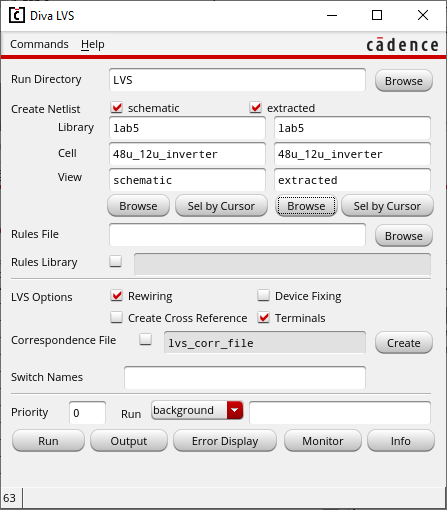
Now to setup for the LVS check.

https://cmosedu.com/jbaker/courses/ee421L/f23/students/gomezl6/lab5/Pictures/6.png

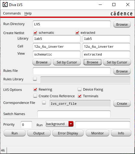
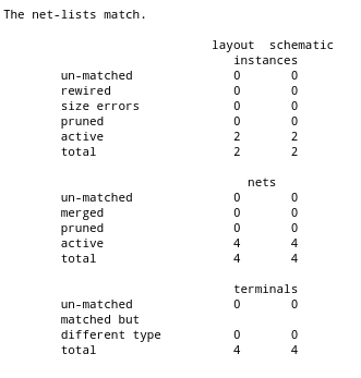
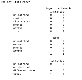
Now running the LVS we get a match.

https://cmosedu.com/jbaker/courses/ee421L/f23/students/gomezl6/lab5/Pictures/7.png

https://cmosedu.com/jbaker/courses/ee421L/f23/students/gomezl6/lab5/Pictures/8.png

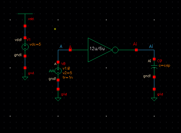
Now I setup a schematic using the symbol which will be used to simulate.

https://cmosedu.com/jbaker/courses/ee421L/f23/students/gomezl6/lab5/Pictures/9.png

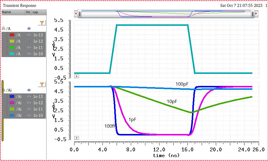
First, I run the simulation using the spectre simulator 

https://cmosedu.com/jbaker/courses/ee421L/f23/students/gomezl6/lab5/Pictures/10.png

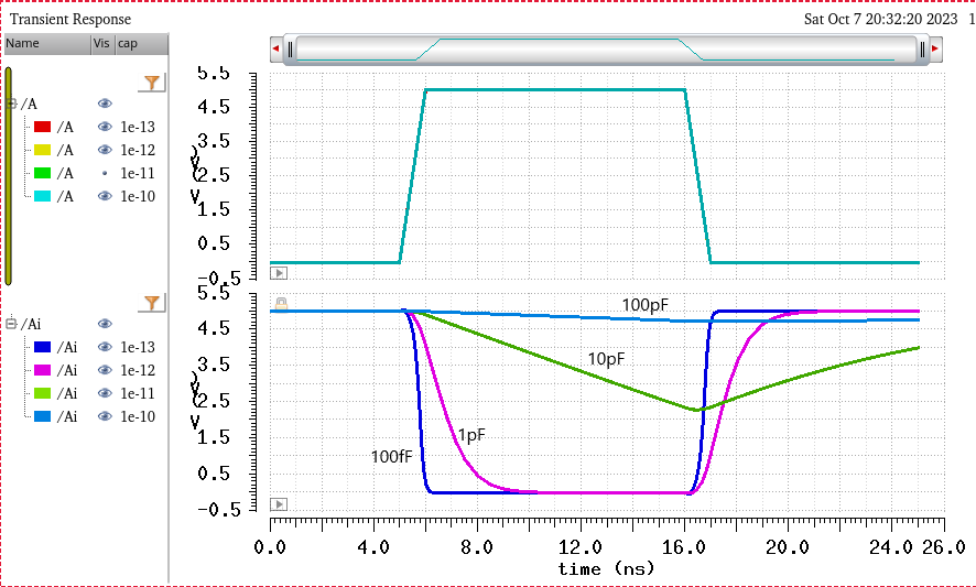
Then, we run the simulation again using the UltraSim 

https://cmosedu.com/jbaker/courses/ee421L/f23/students/gomezl6/lab5/Pictures/11.png

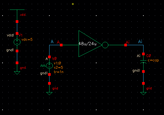
Now we go onto the next inverter which is a 48u/24u using a multiplier of 4. First, we start off with the schematic.

https://cmosedu.com/jbaker/courses/ee421L/f23/students/gomezl6/lab5/Pictures/12.png

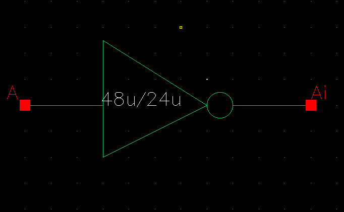
Now, we convert the schematic into a symbol. 

https://cmosedu.com/jbaker/courses/ee421L/f23/students/gomezl6/lab5/Pictures/13.png

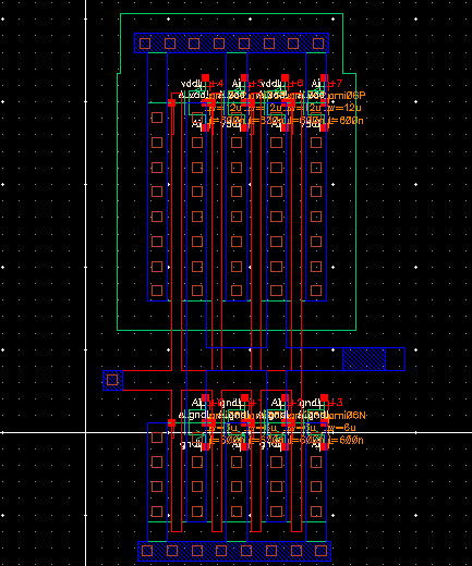
Now we make the layout for the inveter 

https://cmosedu.com/jbaker/courses/ee421L/f23/students/gomezl6/lab5/Pictures/14.png

DRC clean 

https://cmosedu.com/jbaker/courses/ee421L/f23/students/gomezl6/lab5/Pictures/15.png

Now to extract the layout so that we can LVS.

https://cmosedu.com/jbaker/courses/ee421L/f23/students/gomezl6/lab5/Pictures/16.png

Now to setup the LVS.

https://cmosedu.com/jbaker/courses/ee421L/f23/students/gomezl6/lab5/Pictures/17.pnghttps://cmosedu.com/jbaker/courses/ee421L/f23/students/gomezl6/lab5/Pictures/17.png

Running the LVS gives us a match.

https://cmosedu.com/jbaker/courses/ee421L/f23/students/gomezl6/lab5/Pictures/18.png

https://cmosedu.com/jbaker/courses/ee421L/f23/students/gomezl6/lab5/Pictures/19.pnghttps://cmosedu.com/jbaker/courses/ee421L/f23/students/gomezl6/lab5/Pictures/19.png

Now to make the schematic that will be used for simulating.

https://cmosedu.com/jbaker/courses/ee421L/f23/students/gomezl6/lab5/Pictures/20.png

First, we simulate using spectre.

https://cmosedu.com/jbaker/courses/ee421L/f23/students/gomezl6/lab5/Pictures/21.png

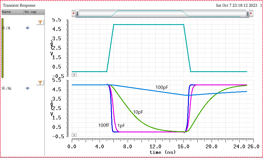
Now, we simulate using UltraSim.

https://cmosedu.com/jbaker/courses/ee421L/f23/students/gomezl6/lab5/Pictures/22.png

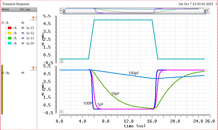
Based on the simulations, it seems that as you increase the capacitace, the output transitions slower. Comparing the two inverters, it seems that the size of the MOSFET also affects the output with the smaller one transitioning slower because of the higher resistance and the larger one transitioning faster becuase their isn't as much resistance. 

Here is a zip file of my work.

Lab5_lg.zip

Return to my Labs 

Return to EE421L Labs