Lab 4 - EE 421L 

Authored by Larri Gomez, gomezl6@unlv.nevada.edu

September 20, 2023 


Lab description

In this lab we learn about the characteristics of the NMOS and PMOS devices by creating schematics and layouts of varying examples. 

Pre Lab 

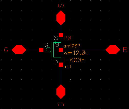
For the pre lab, we are supposed to go through Tutorial 2 which consists on laying out NMOS and PMOS devices. 

We first start off with the NMOS which it has us setting up the layout and the schematic for it. 

https://cmosedu.com/jbaker/courses/ee421L/f23/students/gomezl6/lab4/Pictures/pre1.png


DRC clean
https://cmosedu.com/jbaker/courses/ee421L/f23/students/gomezl6/lab4/Pictures/pre2.png
Now we can setup the schematic which will be used to LVS the layout.
https://cmosedu.com/jbaker/courses/ee421L/f23/students/gomezl6/lab4/Pictures/pre3.png
Now running the LVS we get a match for both.
https://cmosedu.com/jbaker/courses/ee421L/f23/students/gomezl6/lab4/Pictures/pre4.png
Now the same thing is to be done with the PMOS which we start off with the layout.
https://cmosedu.com/jbaker/courses/ee421L/f23/students/gomezl6/lab4/Pictures/pre5.png
DRC clean
https://cmosedu.com/jbaker/courses/ee421L/f23/students/gomezl6/lab4/Pictures/pre6.png
Now the schematic for the PMOS.
https://cmosedu.com/jbaker/courses/ee421L/f23/students/gomezl6/lab4/Pictures/pre7.png
And running the LVS gives a match.
https://cmosedu.com/jbaker/courses/ee421L/f23/students/gomezl6/lab4/Pictures/pre8.png

Lab Work

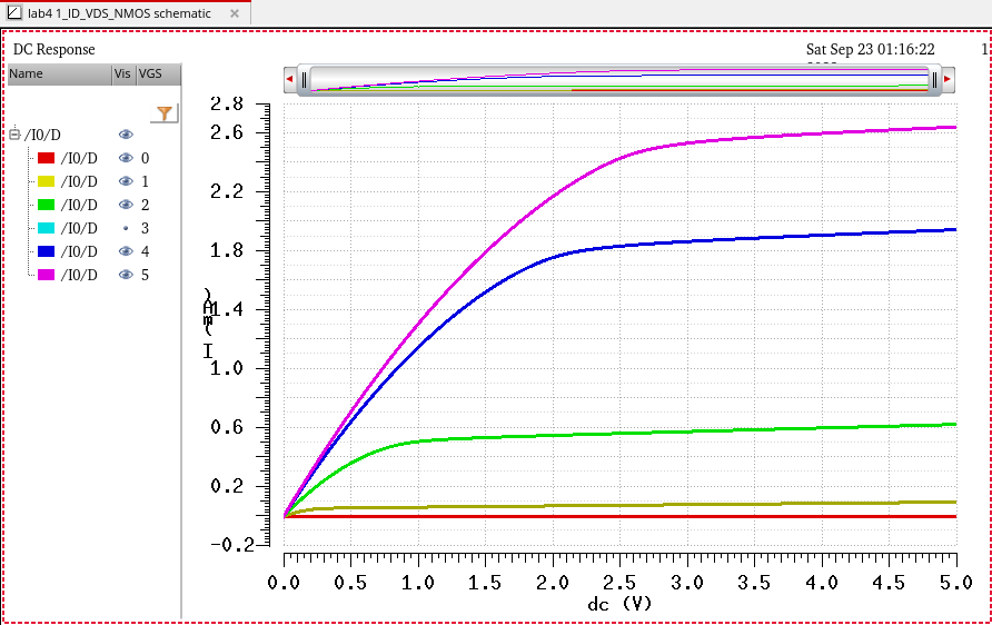
We start off the lab by creating a schematic to simulate a ID vs. VDS for a NMOS device for VGS varying from 0 to 5V in 1V steps and VDS varies from 0 to 5 V in 1 mV steps. The NMOS measures 6u by 0.6u. 

https://cmosedu.com/jbaker/courses/ee421L/f23/students/gomezl6/lab4/Pictures/1.png

Now when we run the simulation this is what we get. 

https://cmosedu.com/jbaker/courses/ee421L/f23/students/gomezl6/lab4/Pictures/2.png

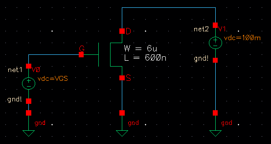
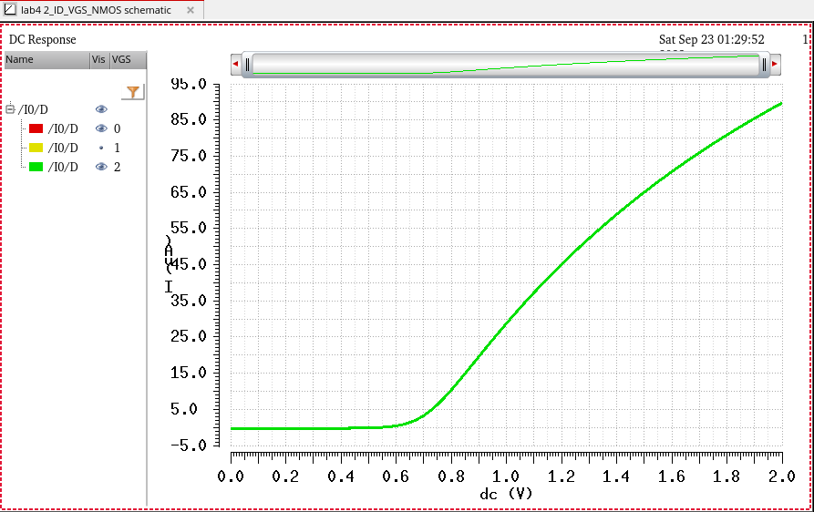
Now we will make a schematic that simulates a ID vs. VGS for a NMOS device for VDS = 100 mV and VGS varies from 0 to 2V in 1 mV steps. The NMOS also measures 6u by 0.6u.

https://cmosedu.com/jbaker/courses/ee421L/f23/students/gomezl6/lab4/Pictures/3.png

This is what we get when running the simulation.

https://cmosedu.com/jbaker/courses/ee421L/f23/students/gomezl6/lab4/Pictures/4.png

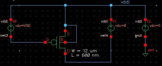
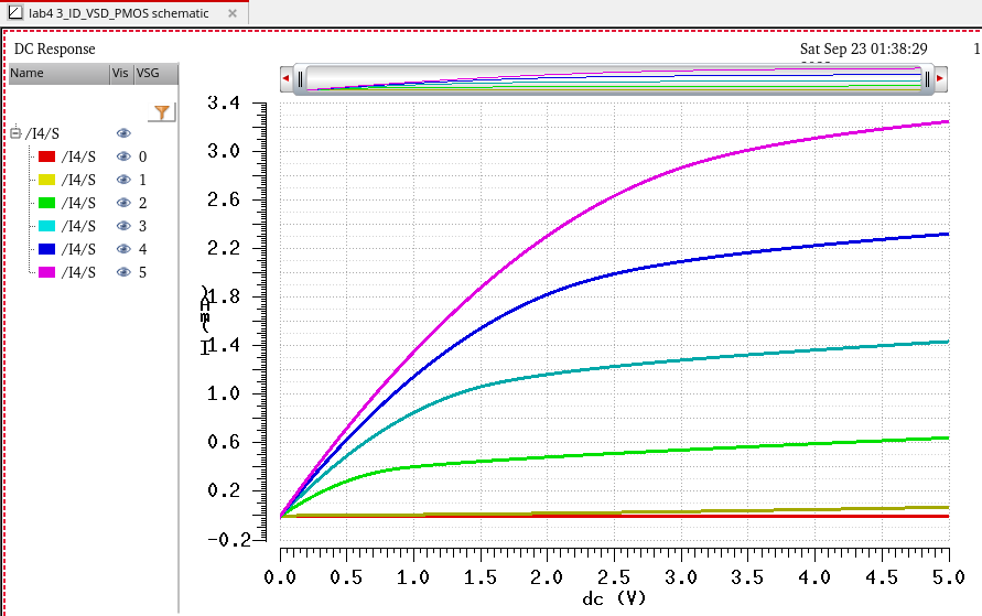
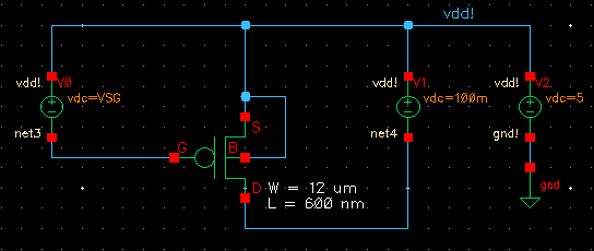
Now we move on to the PMOS which we start off with a schematic to simulate a ID vs. VSD of a PMOS device for VSG that varies from 0 to 5 V in 1 V steps and VSD varies from 0 to 5 in 1 mV steps. The PMOS measures 12u by 0.6u. 

https://cmosedu.com/jbaker/courses/ee421L/f23/students/gomezl6/lab4/Pictures/5.png

This is what I get from the simulation. 

https://cmosedu.com/jbaker/courses/ee421L/f23/students/gomezl6/lab4/Pictures/6.png

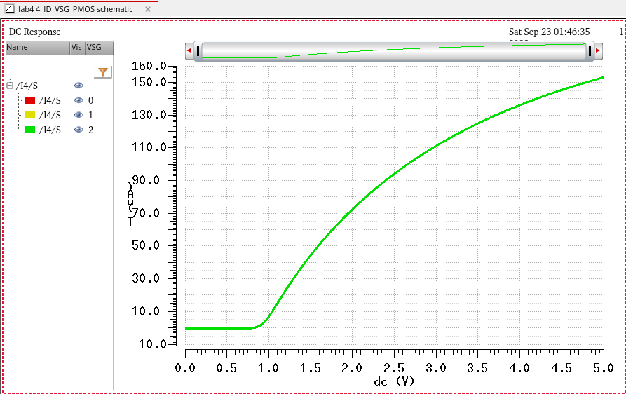
Now we make a schematic that simulates a ID vs. VSG of a PMOS device with VSD = 100 mV and VSG varies from 0 to 2 V in 1 mV steps. The PMOS also measures 12u by 0.6u. 

https://cmosedu.com/jbaker/courses/ee421L/f23/students/gomezl6/lab4/Pictures/7.png

Running the simulation results in this. 

https://cmosedu.com/jbaker/courses/ee421L/f23/students/gomezl6/lab4/Pictures/8.png

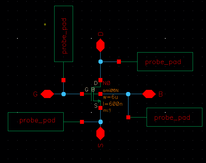
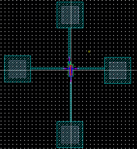
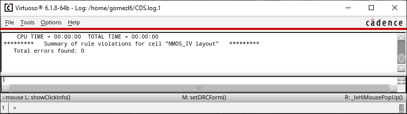
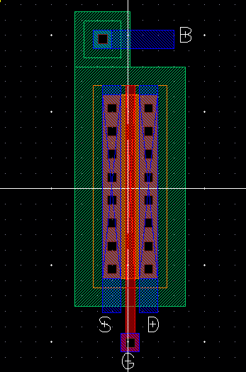
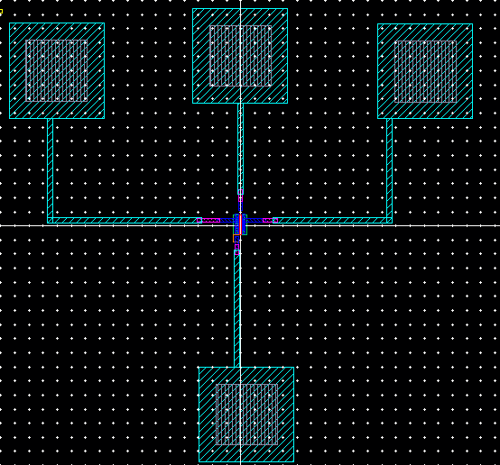
Now we are to layout a 6u by 0.6u NMOS device with all 4 MOSFET terminals connected to probe pads.

https://cmosedu.com/jbaker/courses/ee421L/f23/students/gomezl6/lab4/Pictures/9.png

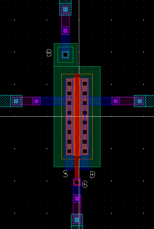
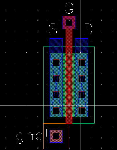
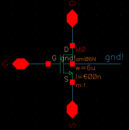
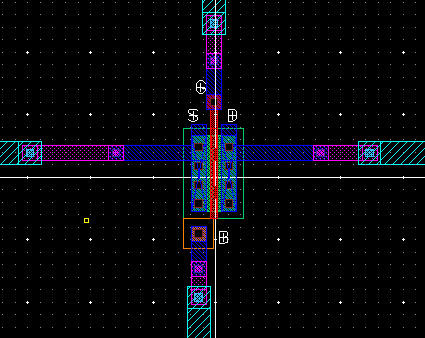
Close up view of the NMOS. 
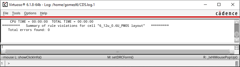
https://cmosedu.com/jbaker/courses/ee421L/f23/students/gomezl6/lab4/Pictures/10.png

DRC clean

https://cmosedu.com/jbaker/courses/ee421L/f23/students/gomezl6/lab4/Pictures/11.png

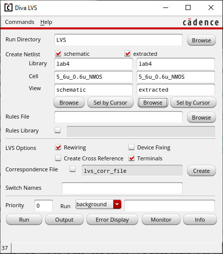
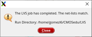
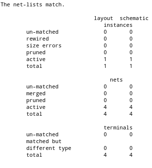
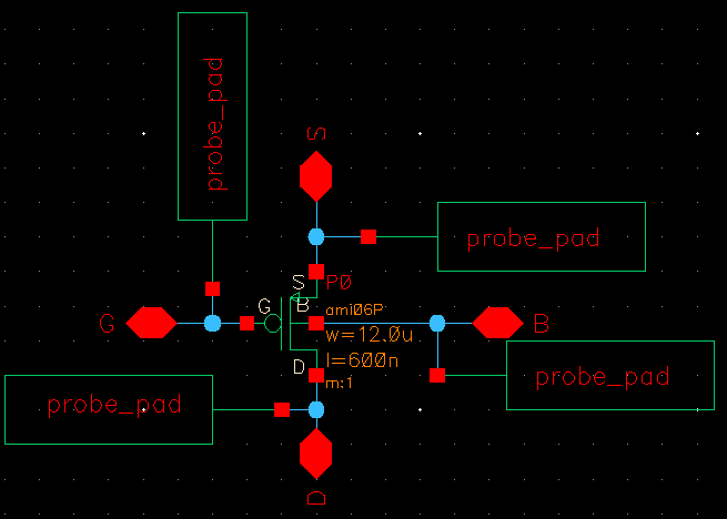
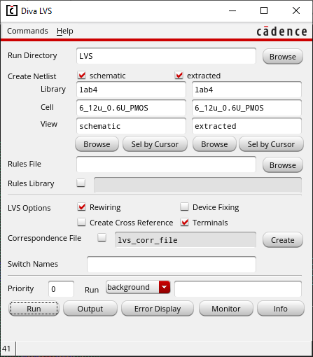
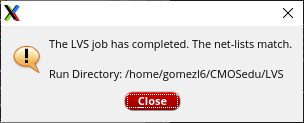
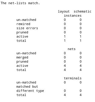
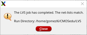
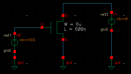
Now to make a corresponding schematic so that we can LVS check it.

https://cmosedu.com/jbaker/courses/ee421L/f23/students/gomezl6/lab4/Pictures/12.png
Now we can run the LVS check with the schematic and extracted view of the layout.
https://cmosedu.com/jbaker/courses/ee421L/f23/students/gomezl6/lab4/Pictures/13.png
We get a match.
https://cmosedu.com/jbaker/courses/ee421L/f23/students/gomezl6/lab4/Pictures/14.png
https://cmosedu.com/jbaker/courses/ee421L/f23/students/gomezl6/lab4/Pictures/15.png
Now we have to create a layout for 12u by 0.6u PMOS device that also connects all 4 MOSFET terminals to probe pads.
https://cmosedu.com/jbaker/courses/ee421L/f23/students/gomezl6/lab4/Pictures/16.png
Close up of the PMOS.
https://cmosedu.com/jbaker/courses/ee421L/f23/students/gomezl6/lab4/Pictures/17.png
DRC clean
https://cmosedu.com/jbaker/courses/ee421L/f23/students/gomezl6/lab4/Pictures/18.png
Now the schematic in order to be able to LVS check.
https://cmosedu.com/jbaker/courses/ee421L/f23/students/gomezl6/lab4/Pictures/19.png
Now running the LVS check.
https://cmosedu.com/jbaker/courses/ee421L/f23/students/gomezl6/lab4/Pictures/20.png
We got a match.
https://cmosedu.com/jbaker/courses/ee421L/f23/students/gomezl6/lab4/Pictures/21.png
https://cmosedu.com/jbaker/courses/ee421L/f23/students/gomezl6/lab4/Pictures/22.png

Return to my Labs 

Return to EE421L Labs