Lab 3 - EE 421L 

Authored by Larri Gomez, gomezl6@unlv.nevada.edu

September 13, 2023


Lab description

This lab will serve as a continuation from lab 2 with us now creating a layout for our 10-bit DAC that we made.


Pre Lab

To start off we are asked to back up our work from the previous labs.

https://cmosedu.com/jbaker/courses/ee421L/f23/students/gomezl6/lab3/Pictures/pre1.png


Now we are supposed to finish with the second half of Tutorial 1 which we can start off by creating the schematic that will be used to create a symbol for the voltage divider.
https://cmosedu.com/jbaker/courses/ee421L/f23/students/gomezl6/lab3/Pictures/pre2.png

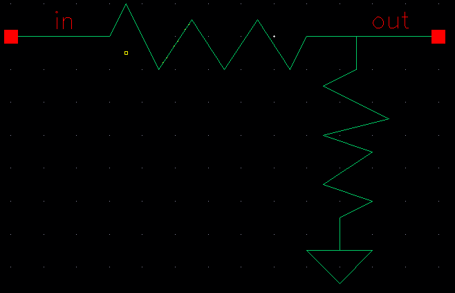
Now we can create the symbol and then go in and draw it out which will look like this. 

https://cmosedu.com/jbaker/courses/ee421L/f23/students/gomezl6/lab3/Pictures/pre3.pnghttps://cmosedu.com/jbaker/courses/ee421L/f23/students/gomezl6/lab3/Pictures/pre3.png

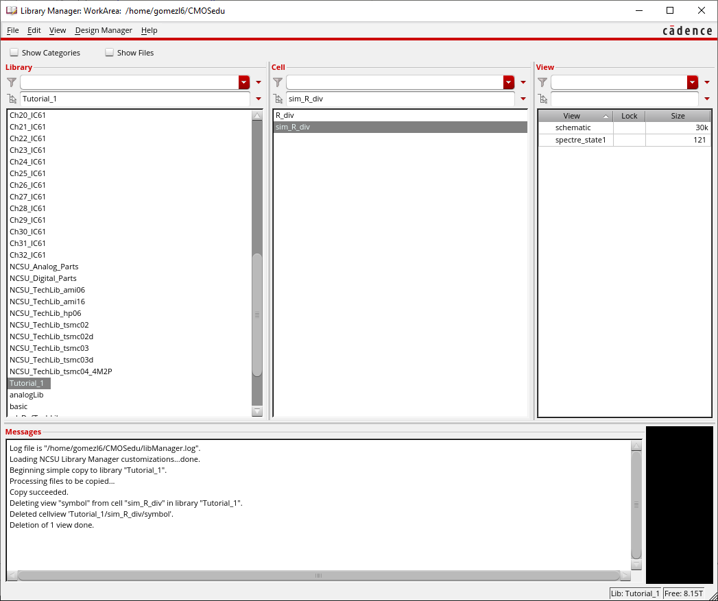
After checking and saving our symbol, we can now try it out to make sure that it works. First, I will make a copy of the R_div cell and call it sim_R_div. 

https://cmosedu.com/jbaker/courses/ee421L/f23/students/gomezl6/lab3/Pictures/pre4.png

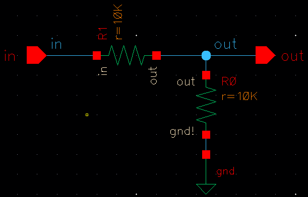
Now we create a schematic that makes use of the newly created symbol. 

https://cmosedu.com/jbaker/courses/ee421L/f23/students/gomezl6/lab3/Pictures/pre5.png

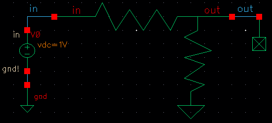
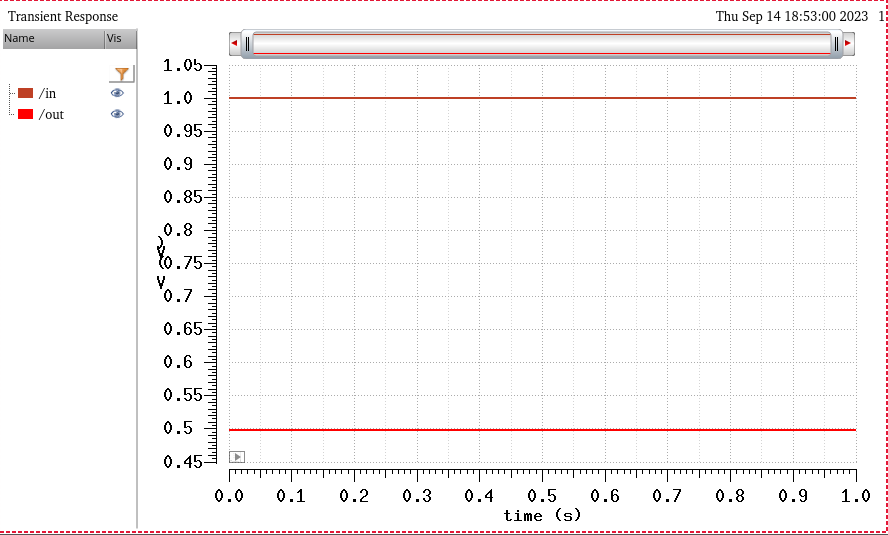
And when running the simulation we end up with the same results we got in the original schematic. 

https://cmosedu.com/jbaker/courses/ee421L/f23/students/gomezl6/lab3/Pictures/pre6.png

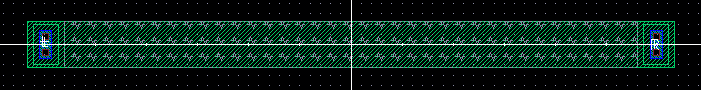
Now we can proceed to make the layout for the schematic but before that, we have to create a layout for a 10k resistor. Our resistor will measure 56.1 for length and 4.5 for width. We also add in the connections on both ends of our box both with 2 contacts and also apply the metal1 on the contacts. To finish it off, we add in the res_id to the center box in order to indicate that it is a resistor. The final setup can be seen below. 

https://cmosedu.com/jbaker/courses/ee421L/f23/students/gomezl6/lab3/Pictures/pre7.png

https://cmosedu.com/jbaker/courses/ee421L/f23/students/gomezl6/lab3/Pictures/clean%20DRC%2010k.png

After making sure that our layout passes DRC, we can then extract our layout and verify that we got the correct resistance.

https://cmosedu.com/jbaker/courses/ee421L/f23/students/gomezl6/lab3/Pictures/pre8.png 

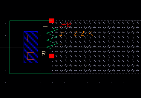
Now using the 10k resistor layout we just made, we can now make the layout for the voltage divider which looks like this. 

https://cmosedu.com/jbaker/courses/ee421L/f23/students/gomezl6/lab3/Pictures/pre9.png 

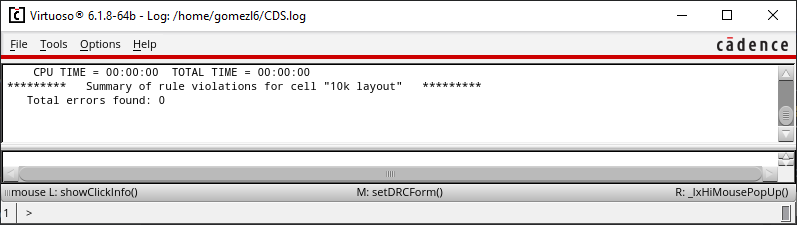
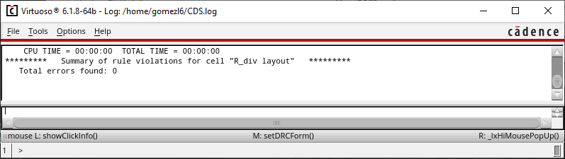
Now I run DRC to check for any errors. 

https://cmosedu.com/jbaker/courses/ee421L/f23/students/gomezl6/lab3/Pictures/pre10.png

Now we have to extract our layout which will be used to verify if it matches up with our schematic using the LVS feature. 

https://cmosedu.com/jbaker/courses/ee421L/f23/students/gomezl6/lab3/Pictures/pre11.png

https://cmosedu.com/jbaker/courses/ee421L/f23/students/gomezl6/lab3/Pictures/pre12.png

Lab Work

Now we will make use of the 10k resistor we just made for our 10-bit DAC layout. The lab asks us to discuss how we select a width and length and how we do that is by choosing a length and width in which L/W * 855 equals the desired resistance with the minimum width allowed being 3.6um. The lab also asks how we can measure the width and length of the resistor. That can be done by using the shortcut key k which will bring up the ruler which we could then use to measure the length and width of the resistor. 

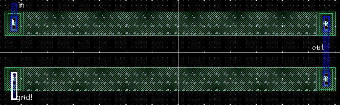
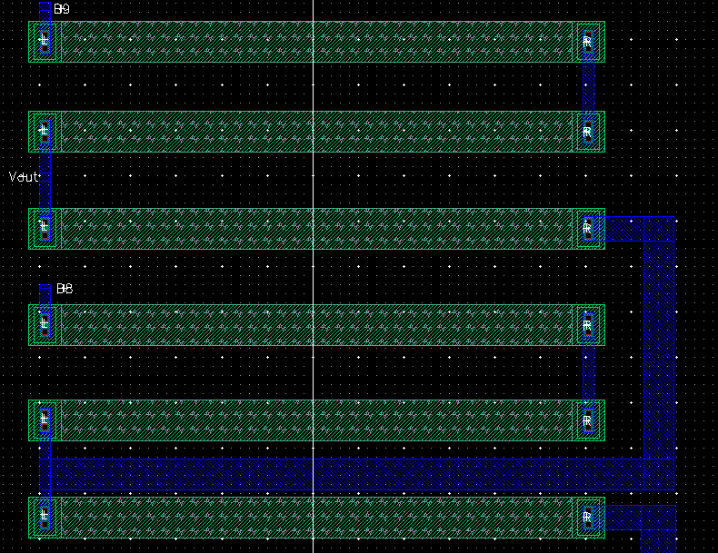
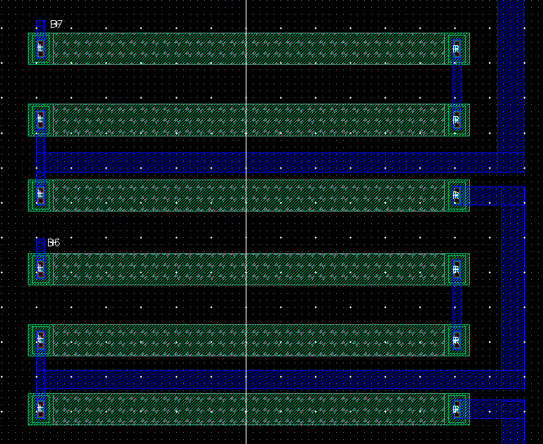
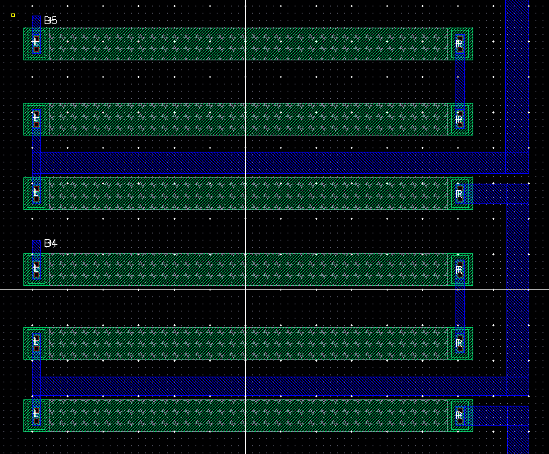
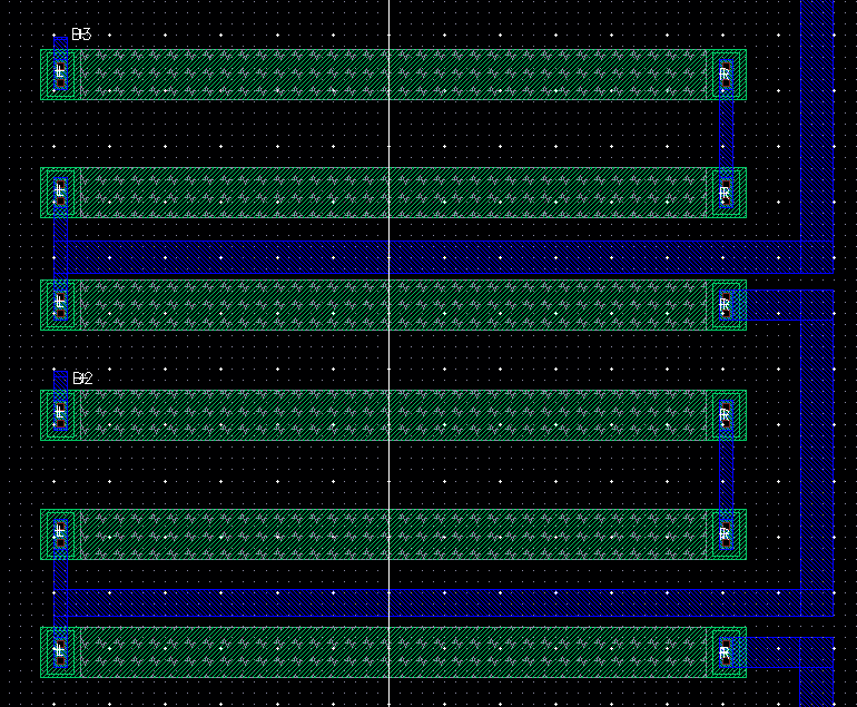
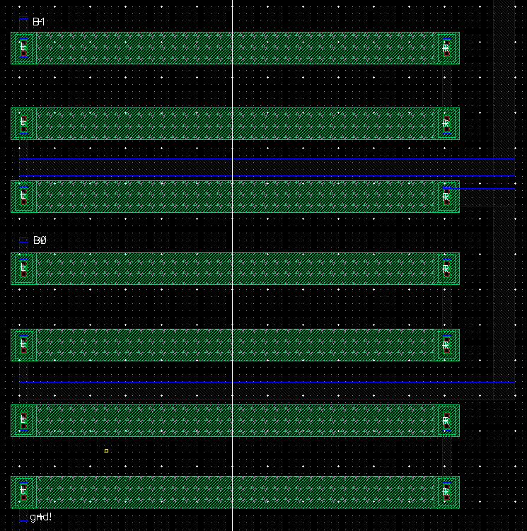
Now to begin with the layout I will lay down resistors in parallel and add in the metal connections for each of the bits.

https://cmosedu.com/jbaker/courses/ee421L/f23/students/gomezl6/lab3/Pictures/1.png

https://cmosedu.com/jbaker/courses/ee421L/f23/students/gomezl6/lab3/Pictures/2.png

https://cmosedu.com/jbaker/courses/ee421L/f23/students/gomezl6/lab3/Pictures/3.png

https://cmosedu.com/jbaker/courses/ee421L/f23/students/gomezl6/lab3/Pictures/4.png

https://cmosedu.com/jbaker/courses/ee421L/f23/students/gomezl6/lab3/Pictures/5.png

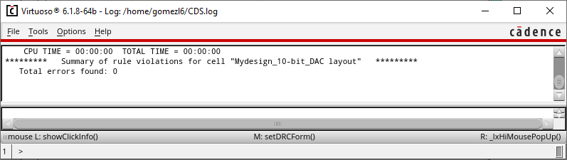
Now we run the DRC check to verify that the layout was setup right.

https://cmosedu.com/jbaker/courses/ee421L/f23/students/gomezl6/lab3/Pictures/6.png

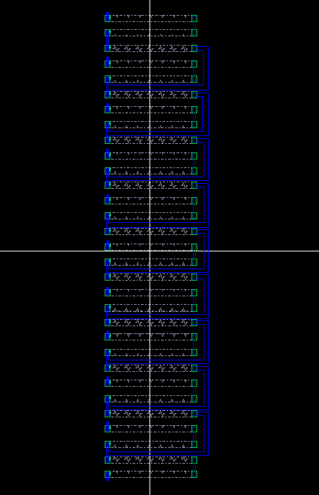
Now we can extract our layout which will look like this. 

https://cmosedu.com/jbaker/courses/ee421L/f23/students/gomezl6/lab3/Pictures/7.png

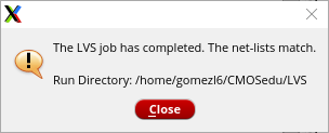
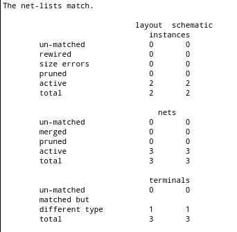
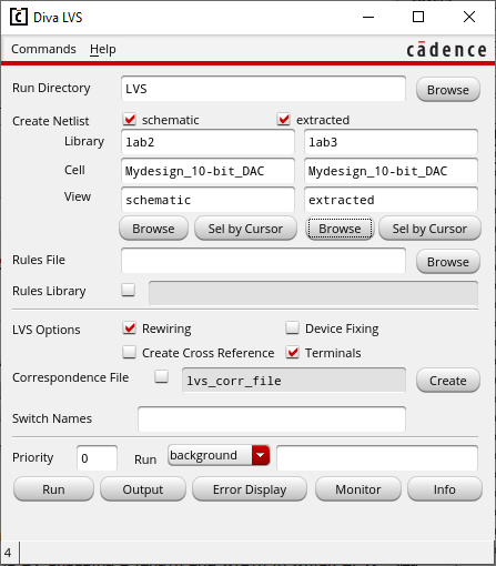
Now we have to run the LVS to ensure that the layout and the schematic match up 

https://cmosedu.com/jbaker/courses/ee421L/f23/students/gomezl6/lab3/Pictures/8.png

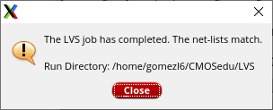
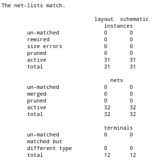
The schematic and layout match up. 

https://cmosedu.com/jbaker/courses/ee421L/f23/students/gomezl6/lab3/Pictures/9.png

https://cmosedu.com/jbaker/courses/ee421L/f23/students/gomezl6/lab3/Pictures/10.png

The zip file of the final design can be seem below which includes lab 2 and 3.

Design Files

Return to my Labs

Return to EE421L Labs