Lab 2 - EE 421L 

Authored by Larri Gomez, gomezl6@unlv.nevada.edu 

September 6, 2023


Lab description

In Lab 2,  we will be designing a 10-bit digital-to-analog converter (DAC) with the use of n-well resistors. 

Pre Lab 

After reading through the entire lab write-up, we start the prelab by downloading the lab2.zip file from the write-up and unzipping in the CMOSedu directory in MobaXterm.

https://cmosedu.com/jbaker/courses/ee421L/f23/students/gomezl6/lab2/Pictures/pre1.jpeg

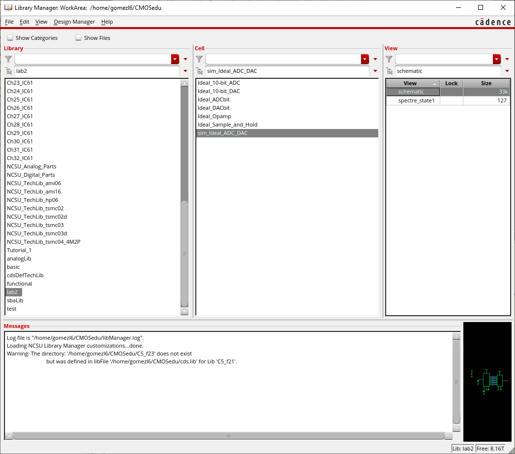
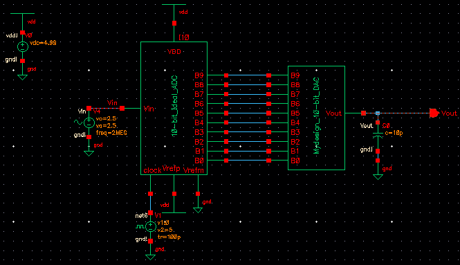
After adding in the DEFINE into the cds.lib file, we can now go into the file manager and open the cell named sim_Ideal_ADC_DAC. 

https://cmosedu.com/jbaker/courses/ee421L/f23/students/gomezl6/lab2/Pictures/pre2.png

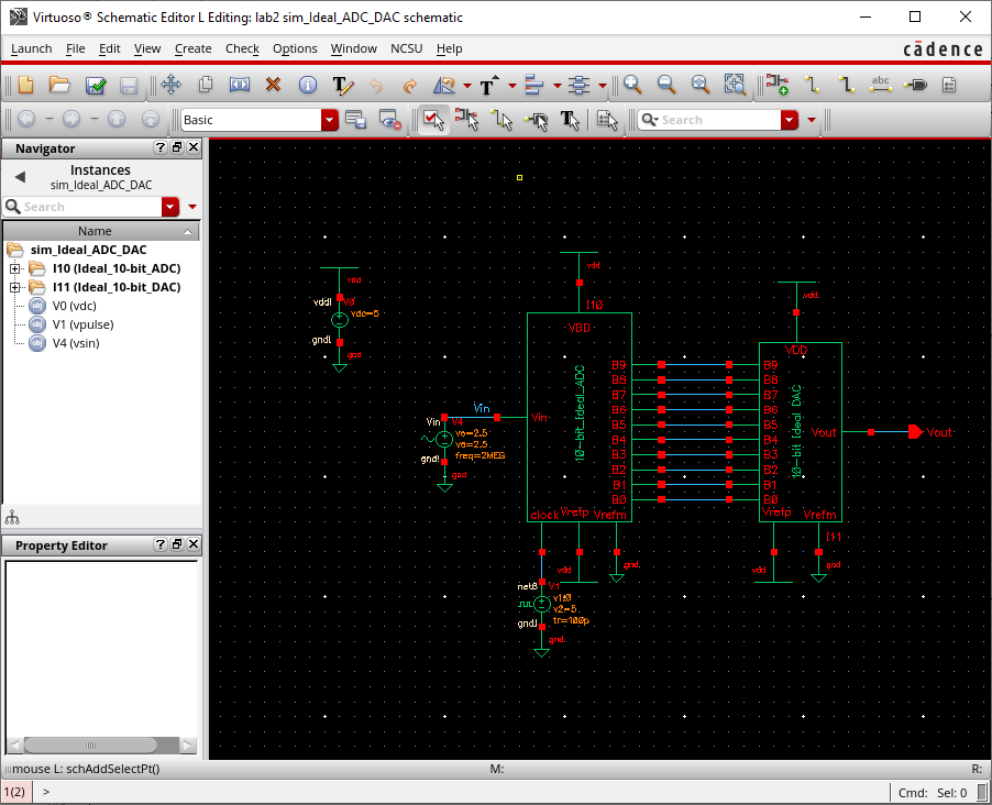
This is how the schematic looks like. 

https://cmosedu.com/jbaker/courses/ee421L/f23/students/gomezl6/lab2/Pictures/pre3.png

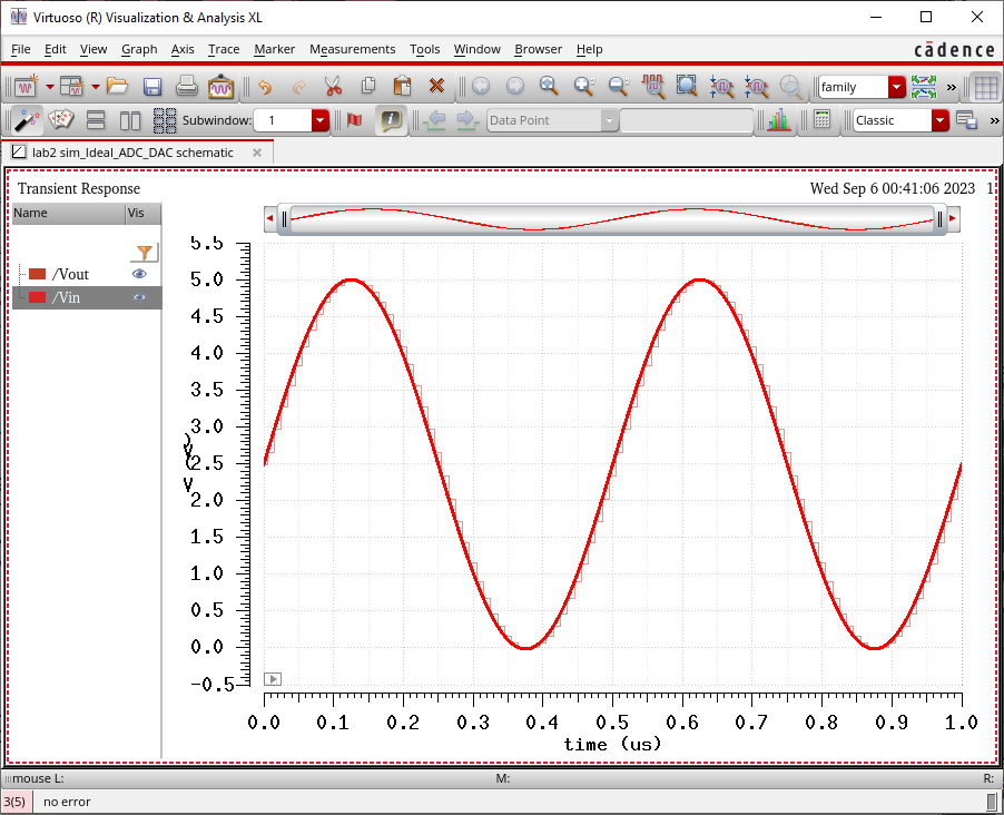
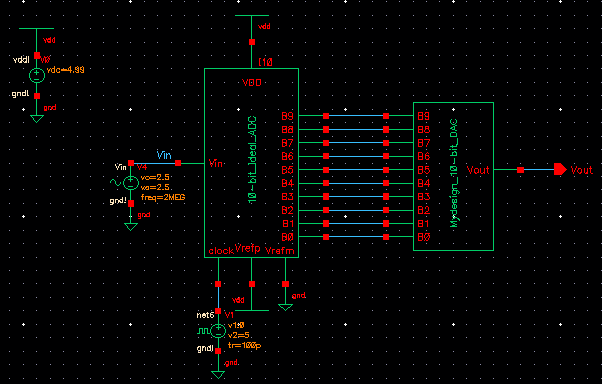
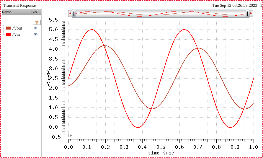
Now we can run ADE L and the simulation looks like this.

https://cmosedu.com/jbaker/courses/ee421L/f23/students/gomezl6/lab2/Pictures/pre4.png
The pre lab also asks for us to understand how the input voltage, Vin, is related to B[9:0] and Vout. How it works is that Vin goes in and converts into steps which can be seen with Vout. For each step, the voltage is rising or falling at a consistent amount. To calculate the minimum voltage needed to see a change in B[9:0], we could use the formula for the LSB which is LSB = Vdd/(2^n) with Vdd being the input which in this case is 5V and n being the number of bits which in this case is 10. Plugging everything in would get you LSB = 5/(2^10) = 0.0048828 V = 4.88mV.

Here I set the Vin to 5mV to get a closer look at each step and how it increases/decreases at 4.88mV per step.
https://cmosedu.com/jbaker/courses/ee421L/f23/students/gomezl6/lab2/Pictures/pre5.png
And if I were to change Vdd to 1V, the minimum voltage I would get is LSB = 1/(2^10) = 0.000976 = 976uV. This is the simulation showing that now each step is increasing/decreasing by 976uV.
https://cmosedu.com/jbaker/courses/ee421L/f23/students/gomezl6/lab2/Pictures/pre6.png

Lab Work

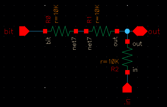
To start off with creating the DAC, first, we make a voltage divider schematic that we could use to make a symbol. 

https://cmosedu.com/jbaker/courses/ee421L/f23/students/gomezl6/lab2/Pictures/1.png

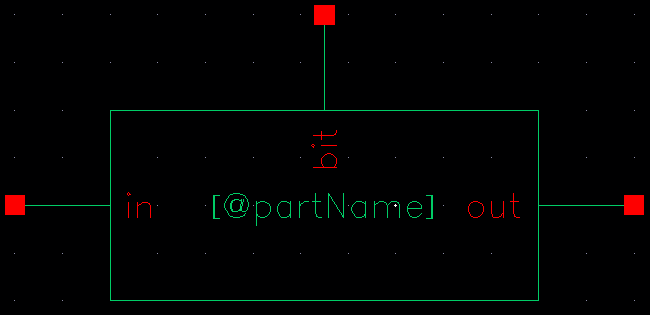
We can then create the symbol which can be seen below. The symbol will work as one bit.

https://cmosedu.com/jbaker/courses/ee421L/f23/students/gomezl6/lab2/Pictures/2.png

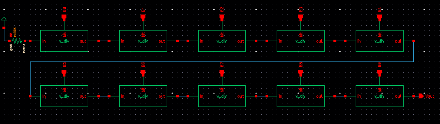
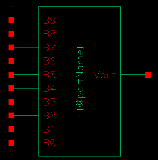
We can now use the created symbol to make the 10-bit DAC. The resulting schematic can be seen below.

https://cmosedu.com/jbaker/courses/ee421L/f23/students/gomezl6/lab2/Pictures/3.png

Then, we are able to create a symbol of our 10-bit DAC schematic.

https://cmosedu.com/jbaker/courses/ee421L/f23/students/gomezl6/lab2/Pictures/4.png

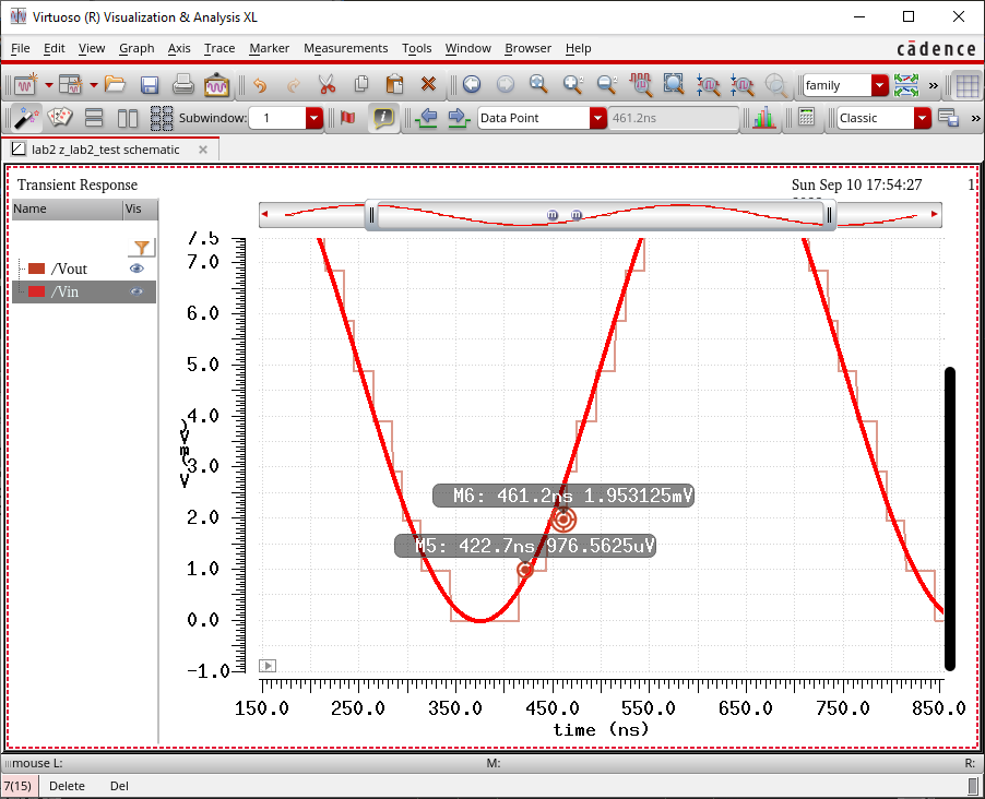
Now, we are suppposed to find the time delay for the DAC which can be done by setting bits 0:8 to ground and then setting 9 to a pulse source. First, I did the hand calculations and ended up getting 70ns.

https://cmosedu.com/jbaker/courses/ee421L/f23/students/gomezl6/lab2/Pictures/5.jpg

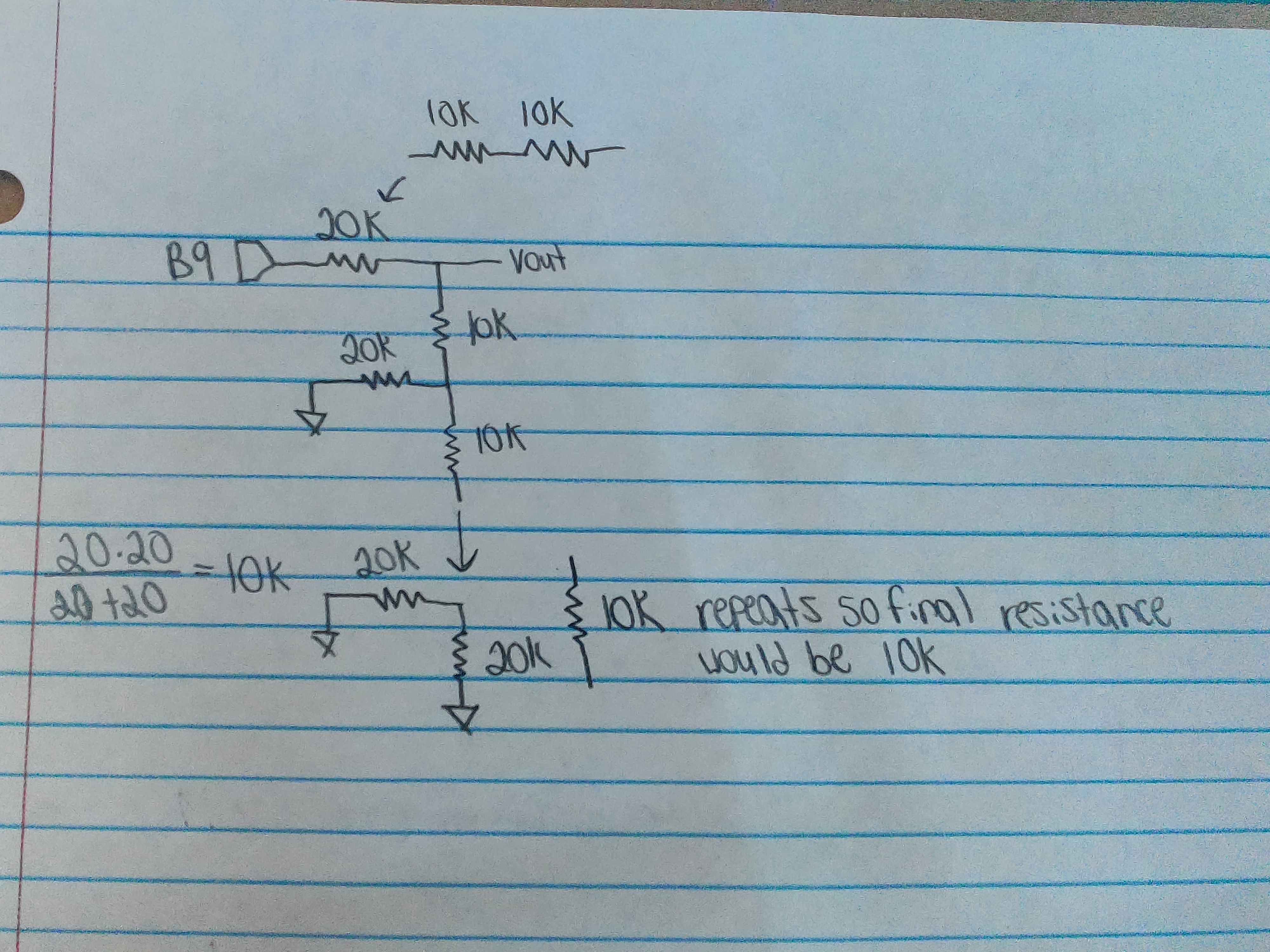
So to solve for the time delay, we will use the resistance we got and also the 10 pF load.

Time Delay = 0.7 (10k)(10pF) = 70ns

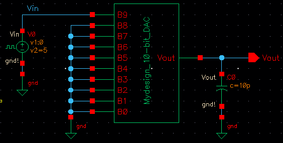
Now to verify our hand calculations using a simulation with our DAC. 

https://cmosedu.com/jbaker/courses/ee421L/f23/students/gomezl6/lab2/Pictures/6.png

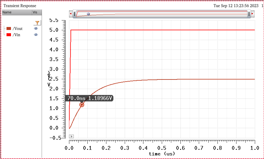
These are the results from the simulation

https://cmosedu.com/jbaker/courses/ee421L/f23/students/gomezl6/lab2/Pictures/7.png

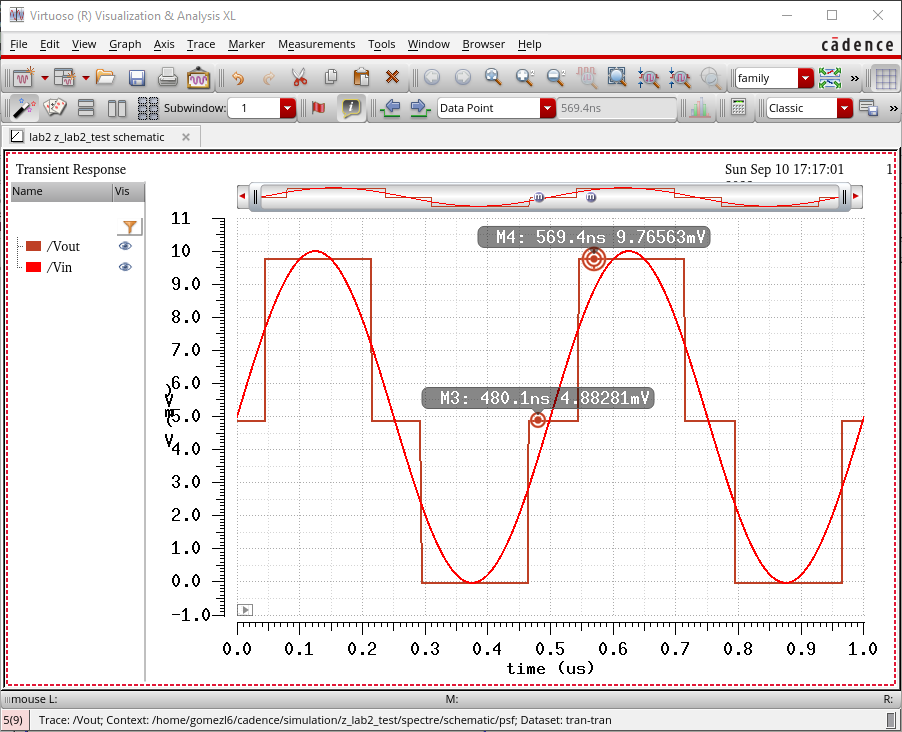
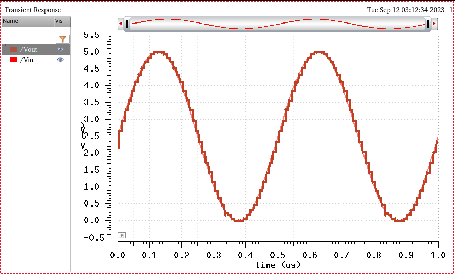
We can now simulate our DAC by replacing the Ideal_10-bit_DAC with ours in the sim_Ideal_ADC_DAC.

https://cmosedu.com/jbaker/courses/ee421L/f23/students/gomezl6/lab2/Pictures/8.png

After running the simulation, we can see that the result is similar to the result we got with the ideal DAC.

https://cmosedu.com/jbaker/courses/ee421L/f23/students/gomezl6/lab2/Pictures/9.png

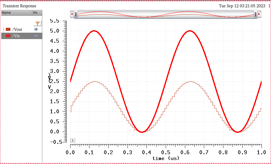
Now lets see what happens if we were to add in a 10k load.

https://cmosedu.com/jbaker/courses/ee421L/f23/students/gomezl6/lab2/Pictures/10.png

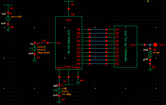
It seems like when adding in the extra 10k load, the voltage output is cut in half of the input voltage. This could be because since the output resistance of the DAC is 10k, adding in the extra 10k resistance resulted in another voltage divider which would explain why the output voltage was halfed. 

https://cmosedu.com/jbaker/courses/ee421L/f23/students/gomezl6/lab2/Pictures/11.png

Now, instead of the extra resistance load, we will now try running it with the 10pF load.

https://cmosedu.com/jbaker/courses/ee421L/f23/students/gomezl6/lab2/Pictures/12.png

It seems like adding in the capacitor smoothened out the output voltage while also creating a delay. 

https://cmosedu.com/jbaker/courses/ee421L/f23/students/gomezl6/lab2/Pictures/13.png

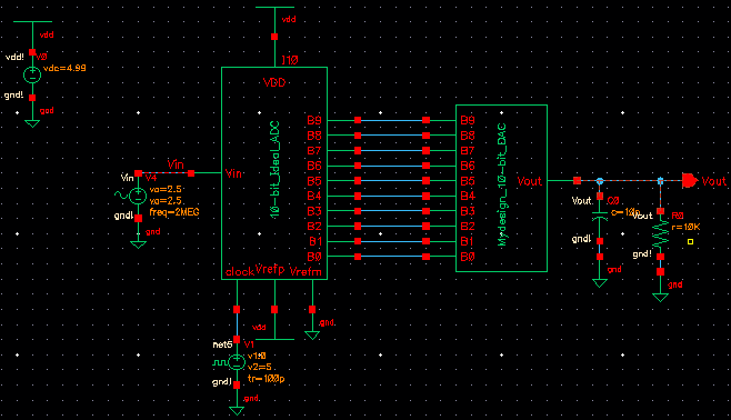
And lastly, we will add in both the resistor and the capacitor. 

https://cmosedu.com/jbaker/courses/ee421L/f23/students/gomezl6/lab2/Pictures/14.png

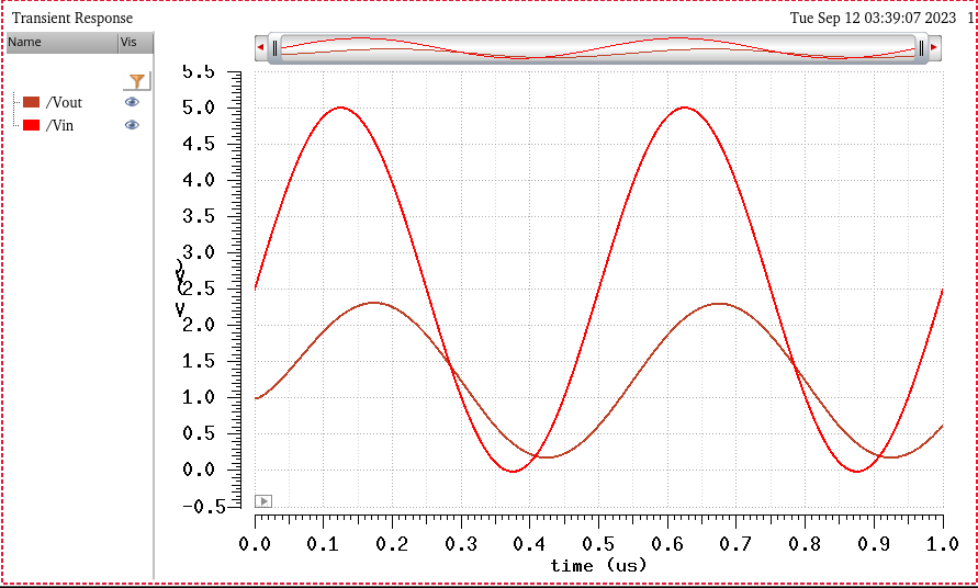
It seems like for this one, the result has a mix of what happened with the resistor and the capacitor with the resistor causing the output voltage to be cut in half while the capacitor smoothened out the curve. 

https://cmosedu.com/jbaker/courses/ee421L/f23/students/gomezl6/lab2/Pictures/15.png

The lab also ask what happens if the resistance of the switches isn't small compared to R in a real circuit. If the switches were to have a high resistance, then we would also have to take into account those values because just like when we added in the extra resistor, it resulted in a lower output voltage. The same thing would occur with the switches with them interfering with the voltage dividers which would then result a smaller voltage. 

Return to my Labs 

Return to EE421L Labs