Lab Project - ECE 421L
Authored
by Kyle Abenojar, abenok1@unlv.nevada.edu
November 22nd, 2023
Jump to Layout
Lab Report:
Project Parameters:
- Non-Inverting Buffer
- Less than 100 fF input capacitance
- Max Load: 1 pF
- Input Logic:
- Logic 0: 1V or less
- Logic 1: 3V or more
- Output Logic:
- Logic 0: ~0V
- Logic 1: >7V
- VDD Range: 4.5V to 5.5V
- Slowest Transition Time: 4ns
Process Used:
The design process used in this project is the C5 0.5 um Process
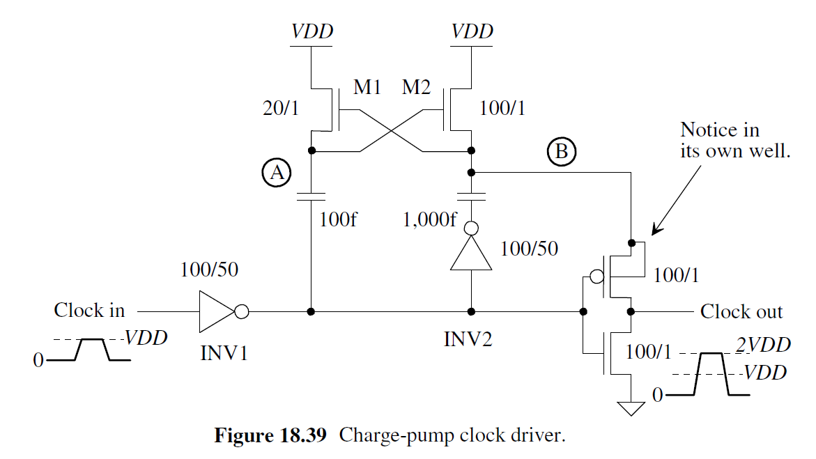
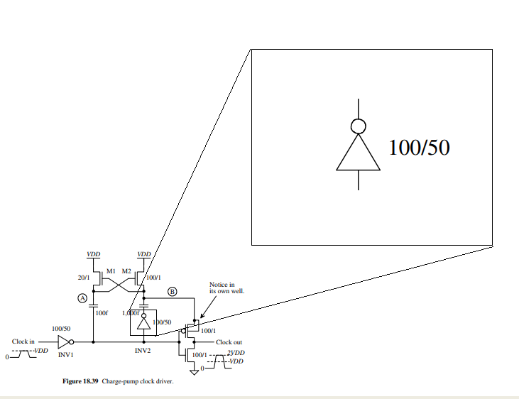
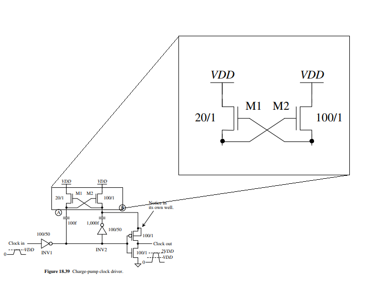
General Design:
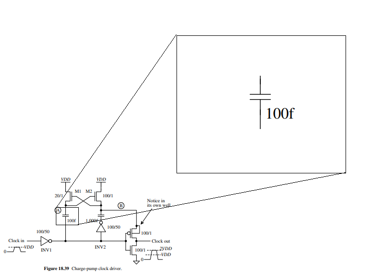
For this project, I based my design off of the charge pump clock driver
seen below. This design was chosen because it fits two main
requirements for the project: 1) For output voltages greater than 7V,
this circuit can output up to 2VDD and 2) Non-Inverting, this circuit
by design is already non-inverting. The other parameters can be
attained by choosing the proper sizing for the capacitors, MOSFETs, and
Inverters.
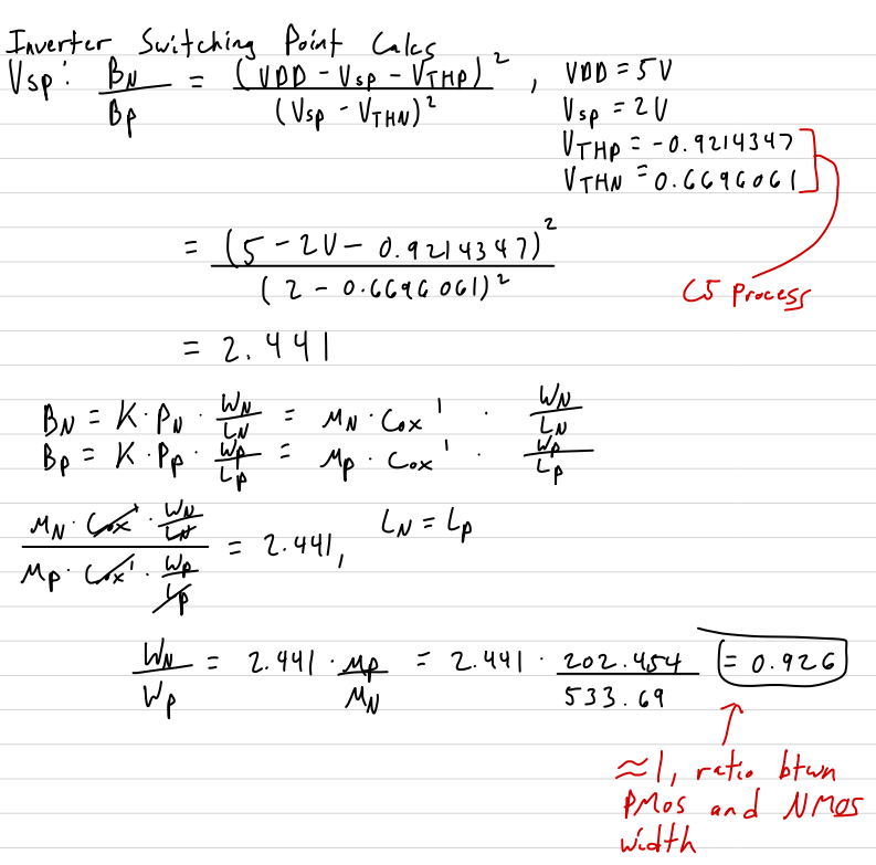
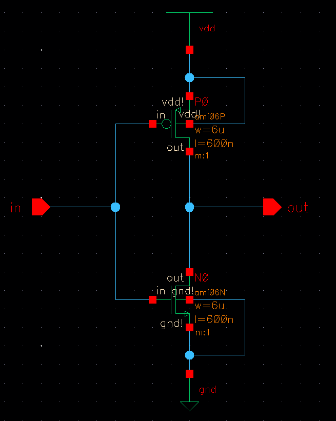
Sizing INV1:
The first step I took
was sizing INV1. This inverter will take in the output from the chip so
it will have to fill two parameters: 1) Decide if the input signal is a logic 0 and logic 1 and 2) Present less than 100fF of input capacitance
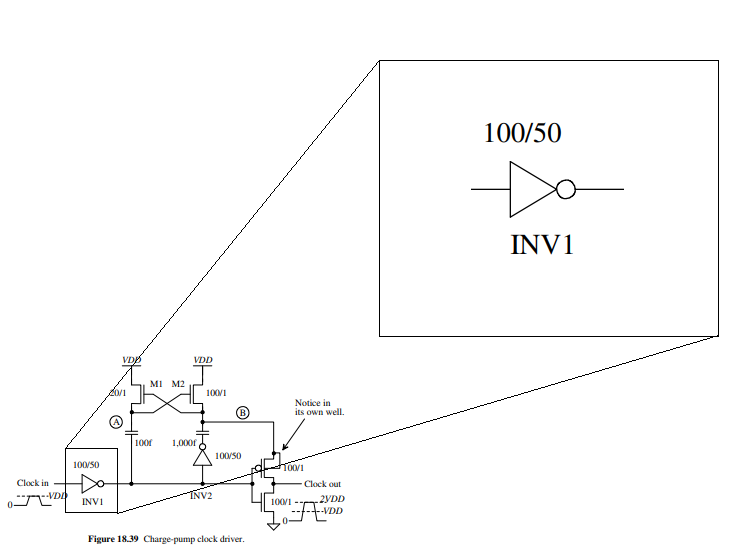
To cover the first requirement, I decided to set the inverters
switching point at 2V. This will place the switching point exactly
between the voltage ranges of a logic high and logic low. Also, since
this is a CMOS inverter, the noise margins will be small enough that we
won't have to worry about them being greater than 1V. So, to make Vsp ~
2V, I made the calculations seen below. To get this switching point,
the ratio between the widths of the NMOS of the PMOS should be 0.926.
For simplicity, I used a ratio of 1.
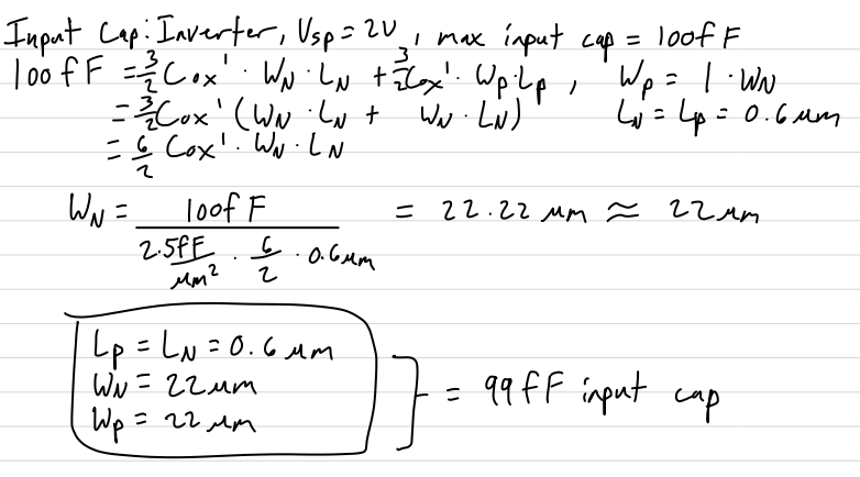
To cover the second
requirement, I calculated the maximum widths I can use for the PMOS and
NMOS of the inverter. Using the minimum length (0.6 um), the biggest
inverter I can use is a 22/22 Inverter, so anything smaller will
suffice. For my design, I used a 6/6 Inverter since I didn't need a
wide inverter for this part of the circuit.
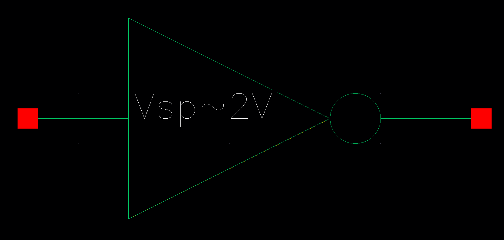
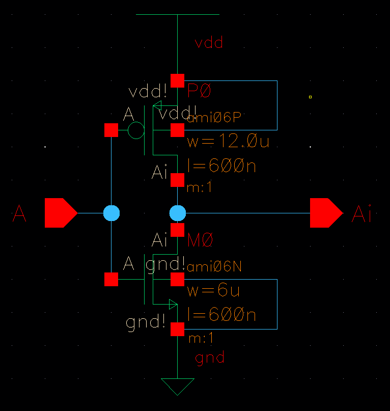
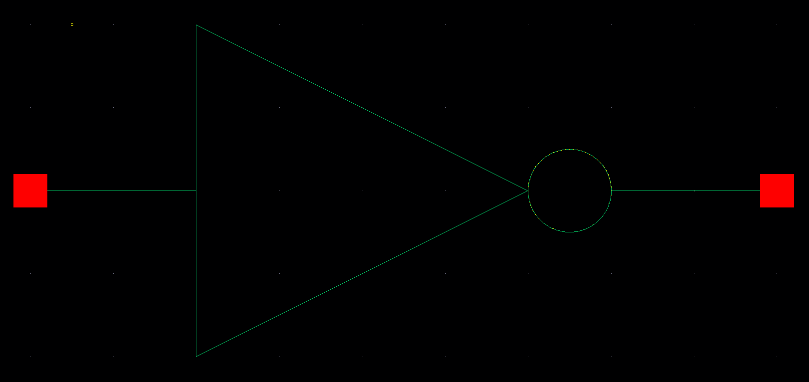
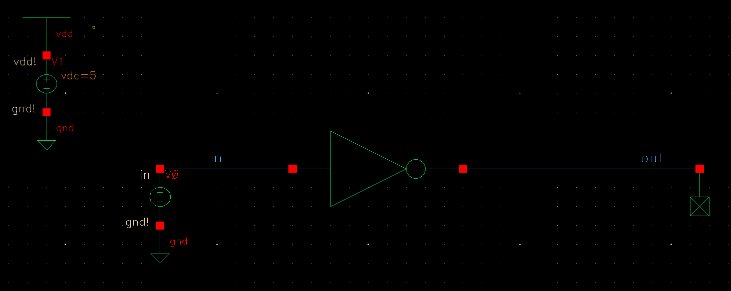
Next, I designed my inverter in cadence. Below are my schematic and symbol.
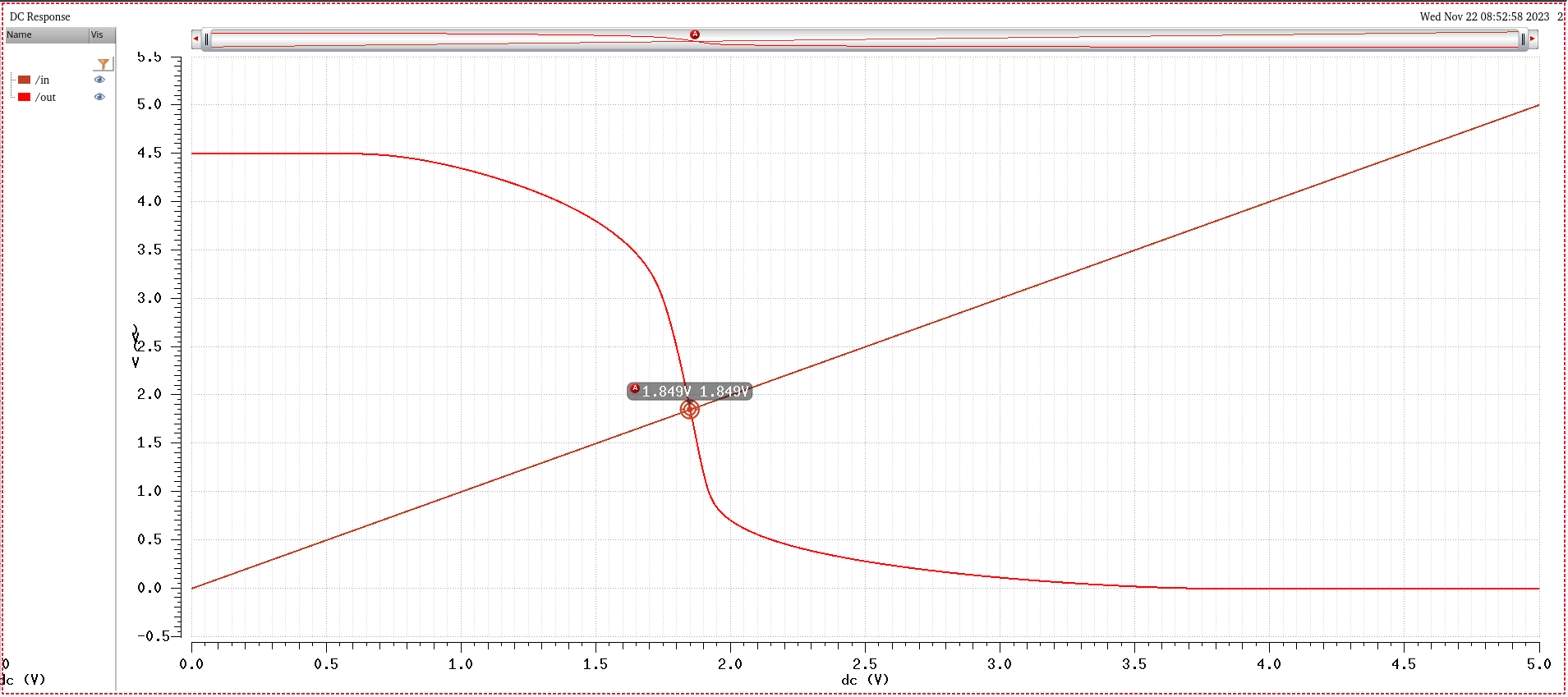
I then tested the operation with the following circuit and performed a dc sweep.
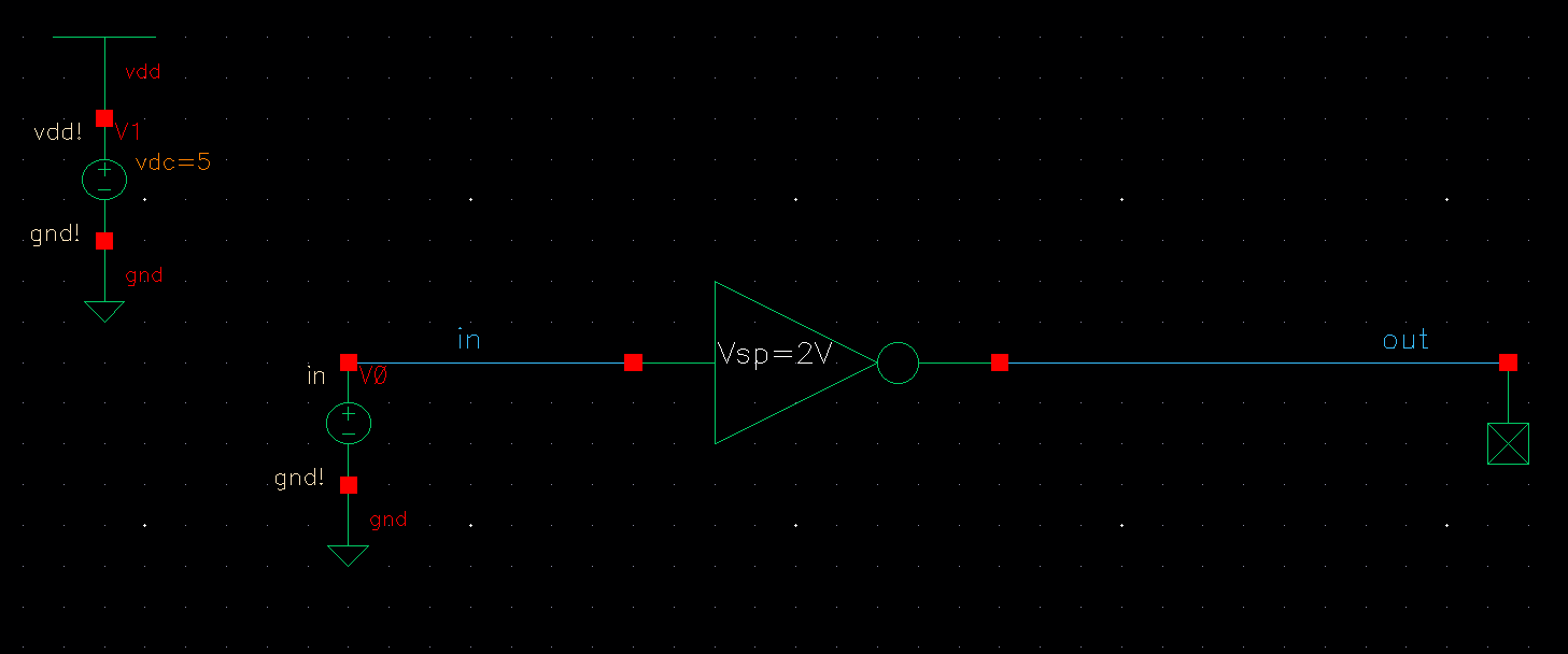
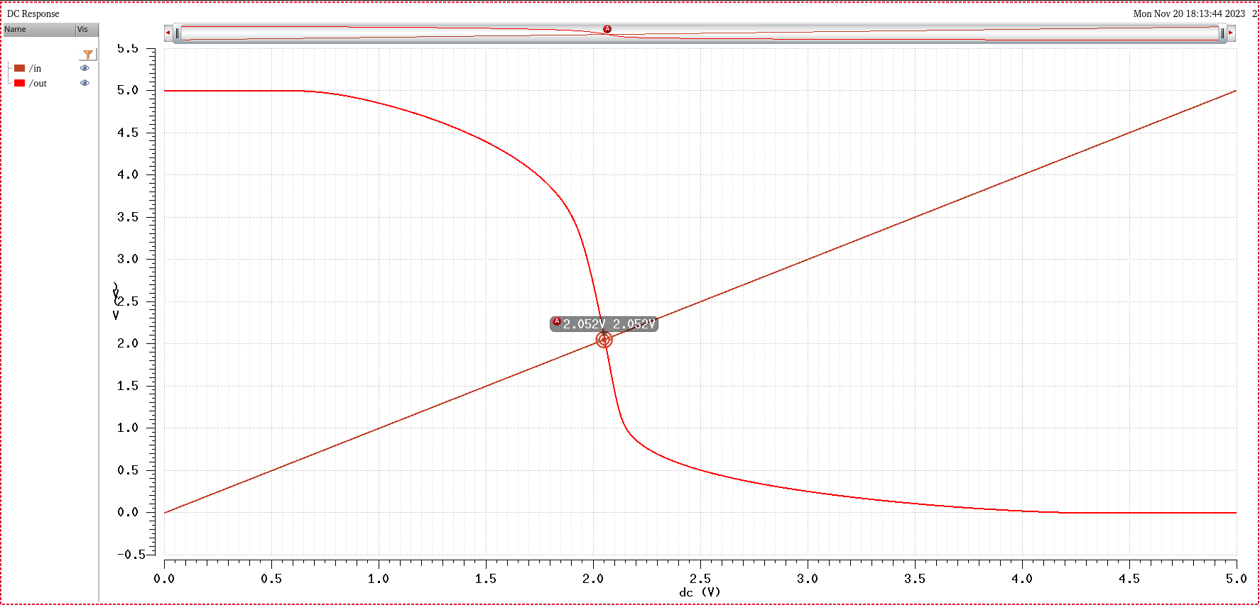
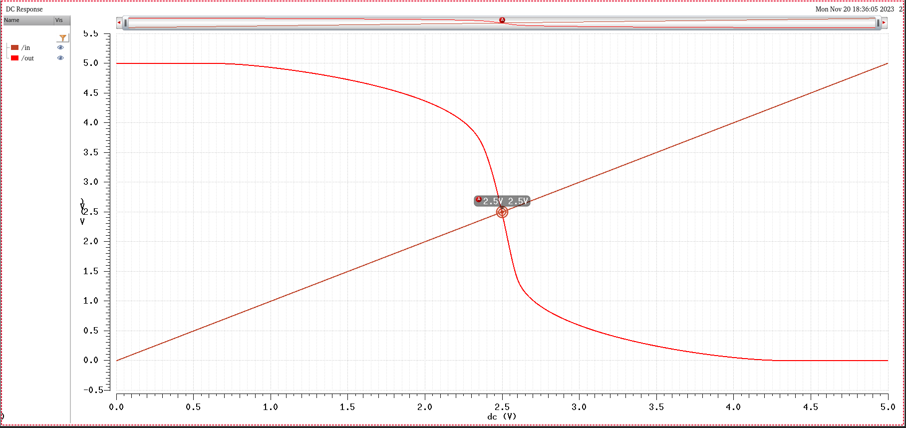
As shown by the output, the Vsp is ~2.052V which is what we expected.
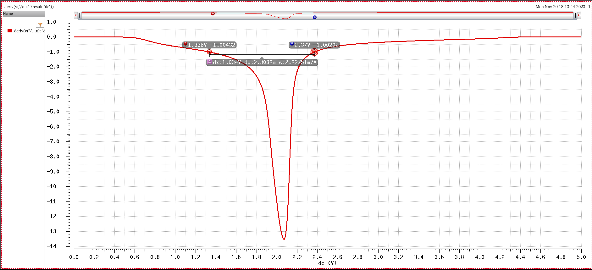
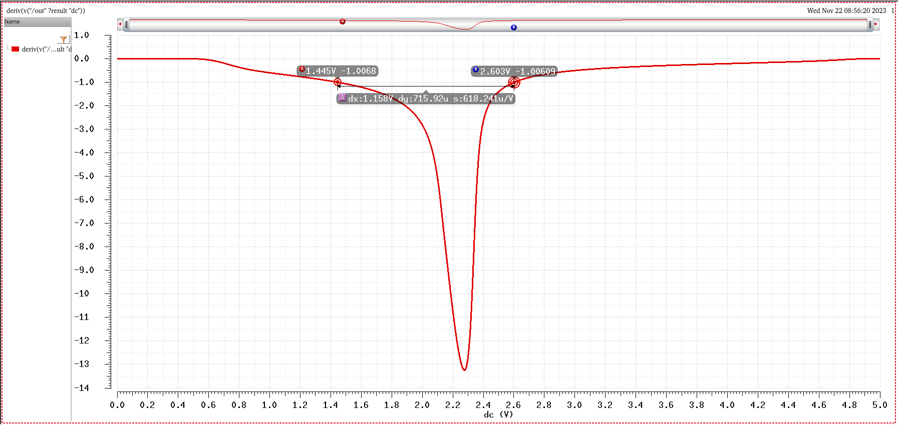
To ensure the input
logic
would work as needed, I took the derivative of the VTC and checked
where the slopes are equal to -1. By definition, this is where Voltage
Input high and low are. As seen below, VIL = ~1.3V and VOH = ~2.4V.
Since VIL > 1V and VOH < 3V, this puts the input and output logic
within spec.
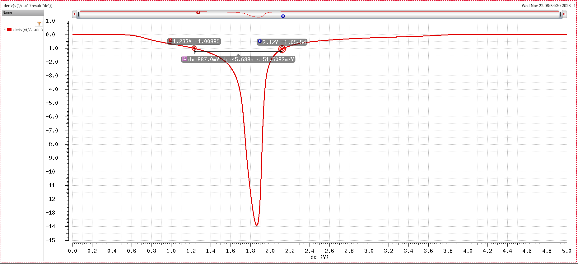
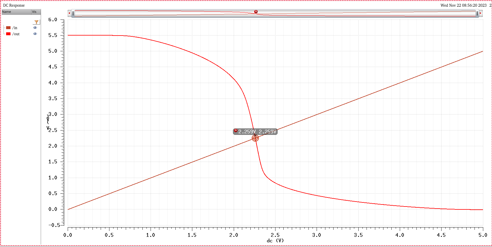
Since
the switching point varies with VDD. I had to check if my inverter
still worked in the ranges of 4.5V to 5.5V. As seen by my results
below, the inverter still functions as it needs to.
VDD = 4.5V
VDD = 5.5V
Sizing INV2:
For inverter 2, its input is the output of inverter 1, so for its
design I just had to set its switching point so that it slices the
output of inverter 1 in half. Inverter 1's output ranges from 0 to 5V
(actual output can range from 4.5V to 5.5V since VDD is not constant,
however 5V is in the middle of this range so I designed for this
value), so inverter 2's switching point will be set at 2.5V. For this
switching point, the resistance of the PMOS and the NMOS has to be
equal. For this process, Rp' is about 2x Rn', so the PMOS should be
twice as wide as the NMOS. For my design, I used a 12/6 inverter, since
again, I don't need a particularly large inverter for this part of the
circuit.
Below are my schematic and symbol for the inverter.
I then tested the operation of this inverter and found that it's switching point is about 2.5V as desired.
Sizing Left Side Capacitor:
Since the left side
capacitor does not supply any power to the output of this circuit, a
small capacitor can be used. For my design, I kept the same value of
100fF. This will help reduce my sizes when I layout my design.
Sizing Right Side Capacitor:
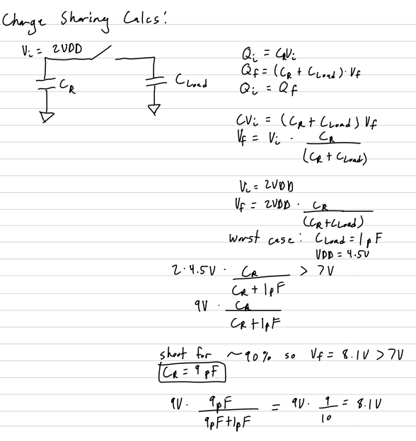
For sizing this capacitor, charge sharing must be considered since it will be providing charge to the output of this circuit.
To find a proper size for this capacitor, I performed charge
sharing calculations between the right side capacitor and capacitive
load in a worst case scenario. For this design, the worst case scenario
will be the lowest VDD (VDD = 4.5V) with the maximum capacitive load (C
= 1pF). For my design, I set my output voltage to about 8V for a worst
case scenario which is above the 7V output parameter. So, for my buffer
the right side capacitor will have a value of 9pF.
Sizing M1 and M2:
M1 is used
to charge the left side capacitor to VDD and M2 is used to charge the
right side capacitor to VDD. Since the left side capacitor is small, M1
can be sized smaller than M2 to minimize layout area and power. A wider
MOSFET means a lower resistance which means a smaller amount of time
required to charge the capacitors. If sized too small, the circuit may
not work properly with fast changing input pulses. For my design, I
kept the same sizing as shown below.
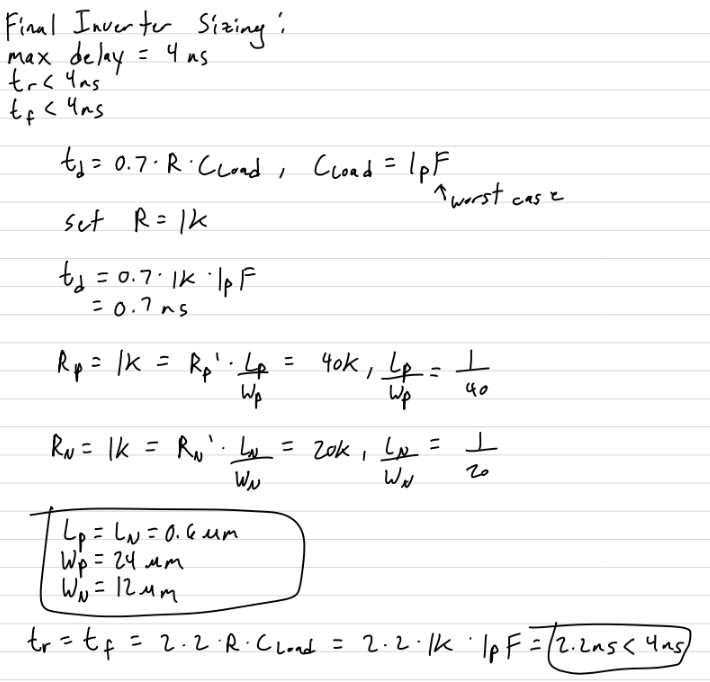
Sizing Output Inverter:
Since this inverter's output will be connected to the capacitive
load, we will have to design around the timing parameter: Slowest Transition Time = 4ns
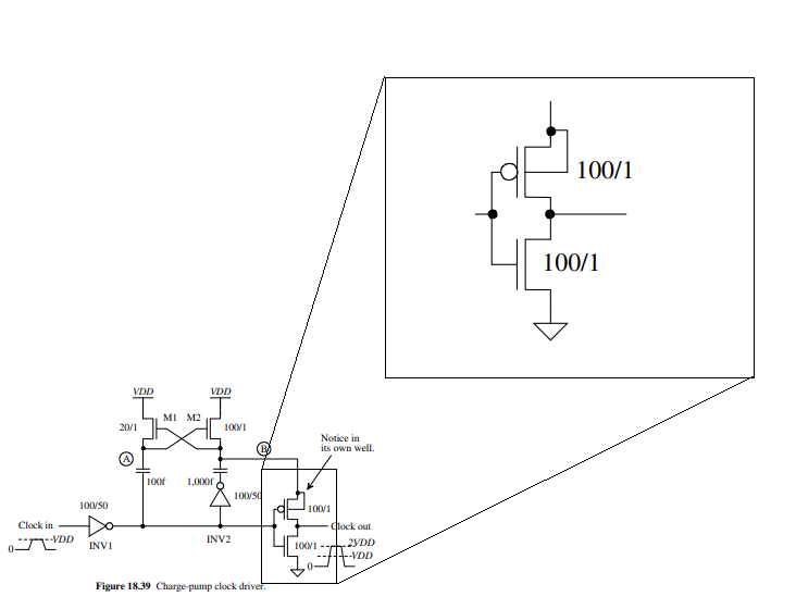
For my design, I chose to design my final inverter to have a
time delay of 0.7ns. With a max load of 1pF, this would mean that the
resistance of the
PMOS and NMOS would have to be around 1k. Using Rp' = 40k and Rn' = 20k
(both overestimates, so the actual operation should be faster than
expected), I performed the calculations below. With these widths, the
rise and fall time should be around 2.2ns which is below the 4ns
requirement. For my design, I used a
24/12 inverter.
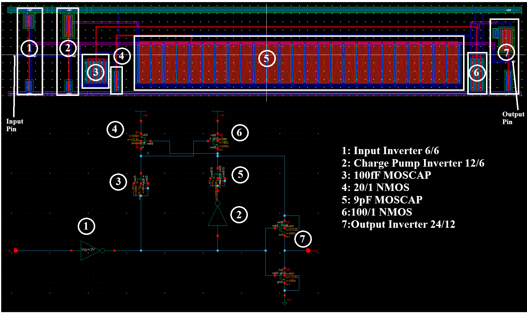
Final Buffer Design:
For my final design for my buffer, I decided to implement my
capacitors using MOSFET's versus using a poly-poly capacitor to reduce
the size of my layout. This is because for a MOSFET, Cox' = 2.5fF/um^2
which is larger than the 900aF/um^2 for a poly-poly capacitor which
means that I can implement the same capacitance with less area. To use
a MOSFET as a capacitor, we can tie the gate to one end and the source,
drain and bulk to another end. To properly size my MOSFET's to get the
right capacitance, I performed the following calculations.
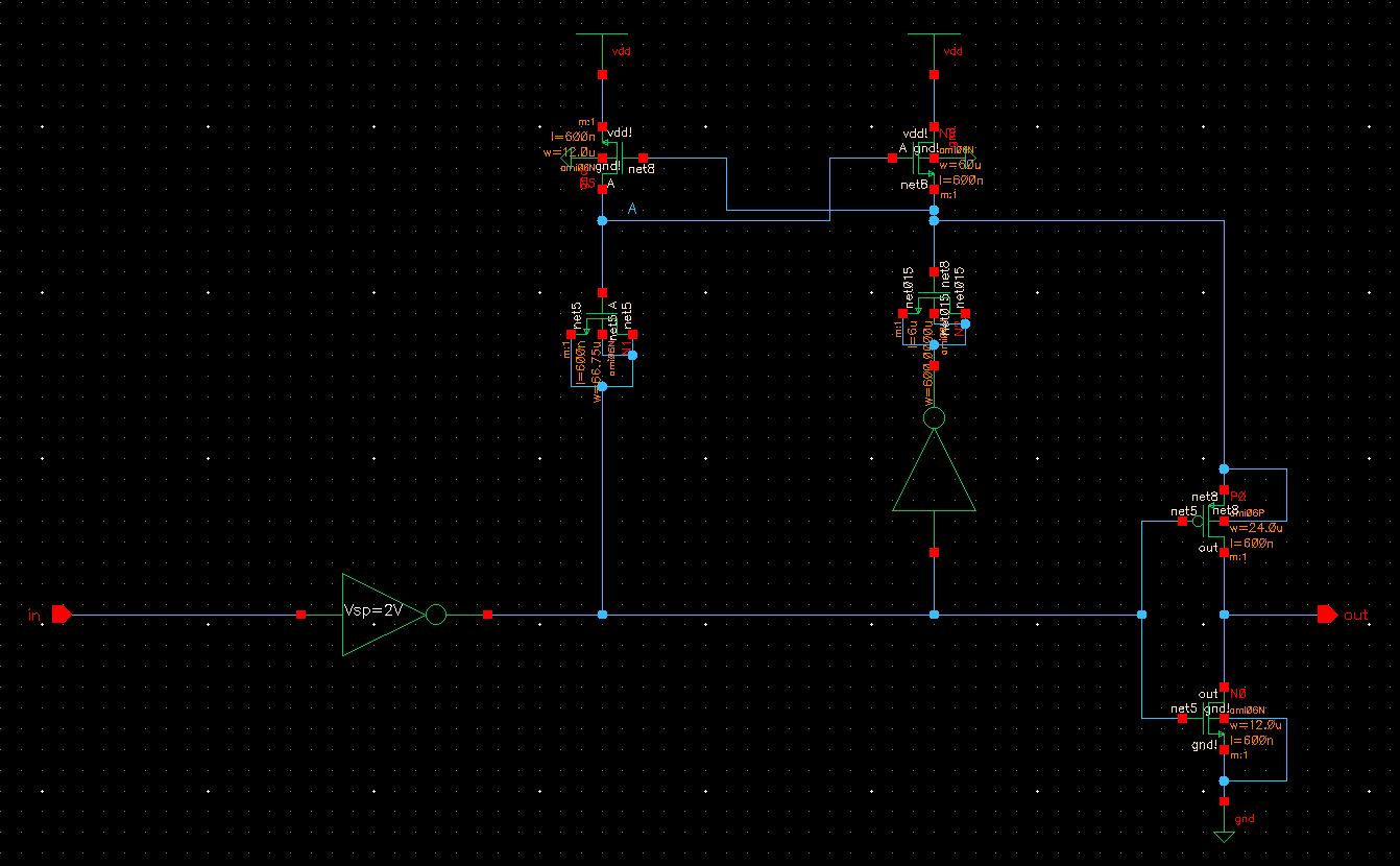
Putting everything together, my final buffer schematic and symbol is
shown below. The MOSFET capacitors are oriented as seen below because
for a MOSFET to maintain a constant capacitance of Cox'*W*L, it must
remain in strong inversion (VGS > VThn). To maintain this, the gate
of the left side capacitor is tied to node A and the gate of the right
side capacitor is tied to node B which always maintain about 1VDD
across the MOSFETs allowing for consistant capacitance. For operation,
this means that nodes A and B will need time to charge up to VDD first
or else the circuit will not operate as expected.
Buffer Operation:
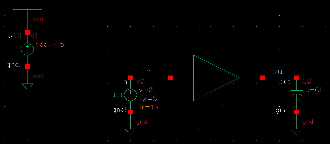
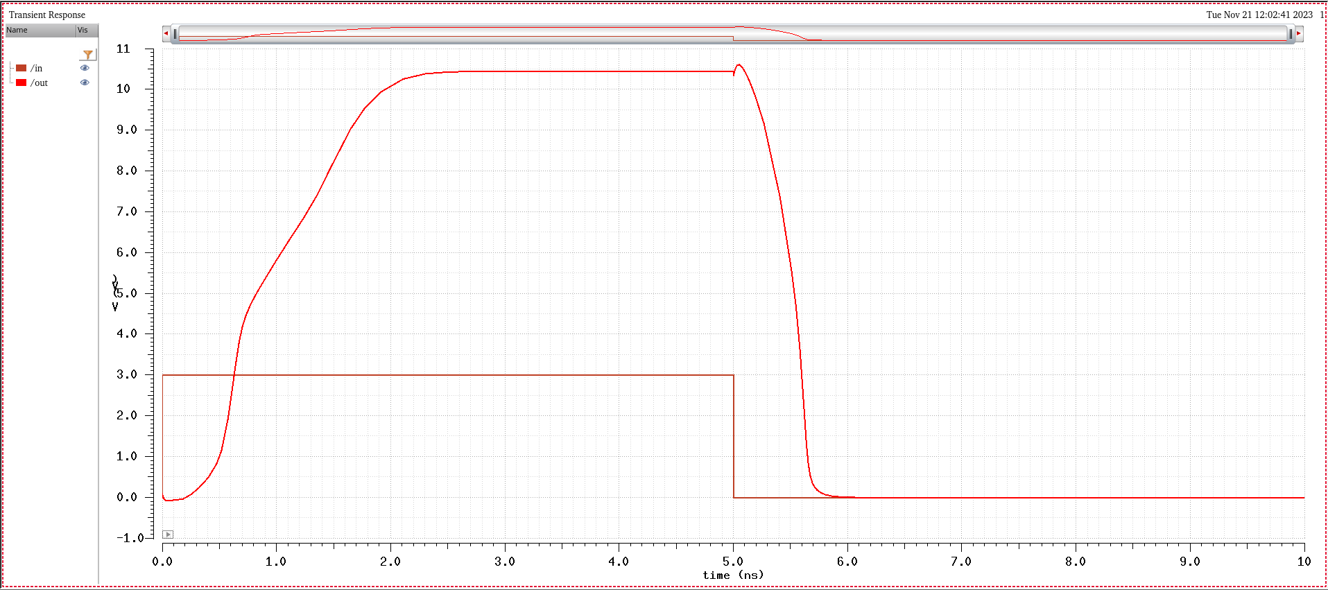
To test my buffer, I used the following schematic and made changes to the values as needed.
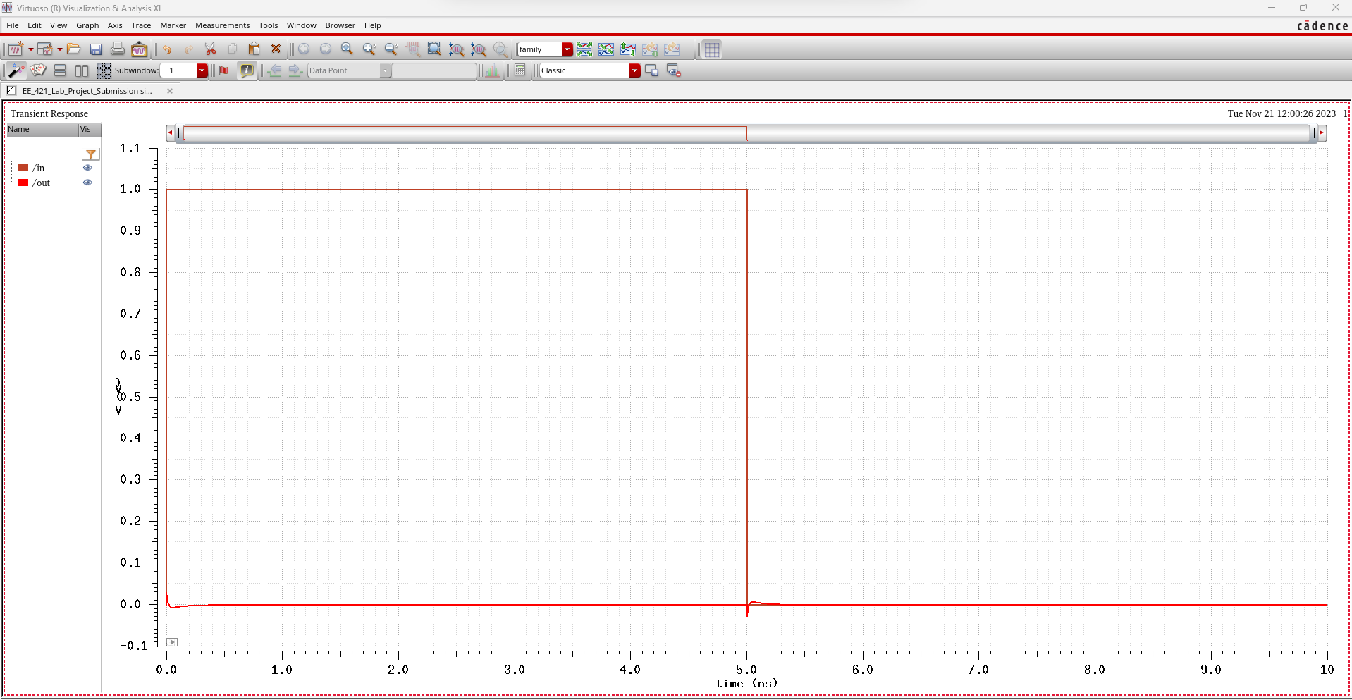
To test my input logic, I
changed the voltages on my input source to check if my buffer detected
0 to 1V as a logic low and if my buffer detected 3V as a logic
high. As shown below, with a 1V input, the output stayed around 0V and
with a 3V input, the output went high as well.
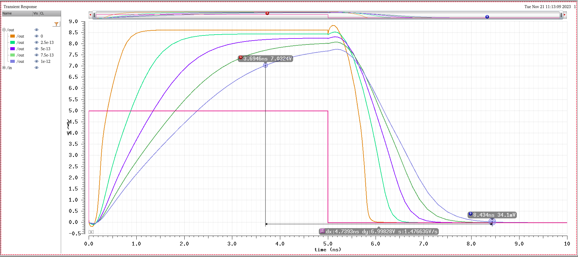
To
test the transition times and output voltage for my buffer, I performed
a parametric analysis with varying VDD, 4.5V, 5V, and 5.5V. For my
parametric analysis, I set the capacitive load to 0, 250fF, 500fF,
750fF and 1pF.
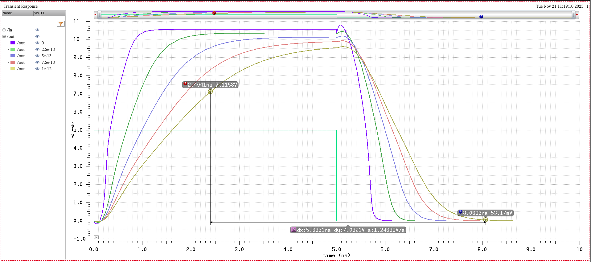
- For
this test, VDD = 4.5V. As we can see below, with a maximum load of 1pF,
the slowest rise time to go above 7V was ~3.7ns and the slowest fall
time was around 3.4ns. We also see that the output voltage goes well above 7V for a logic high and goes to near 0V for a logic low.
- For this test, VDD = 5.0V. As we can see below, with a maximum load of 1pF, the slowest rise
time to go above 7V was ~2.8ns and the slowest fall time was around
3.2ns. We also see that the output voltage goes well above 7V for a logic high and goes to near 0V for a logic low.
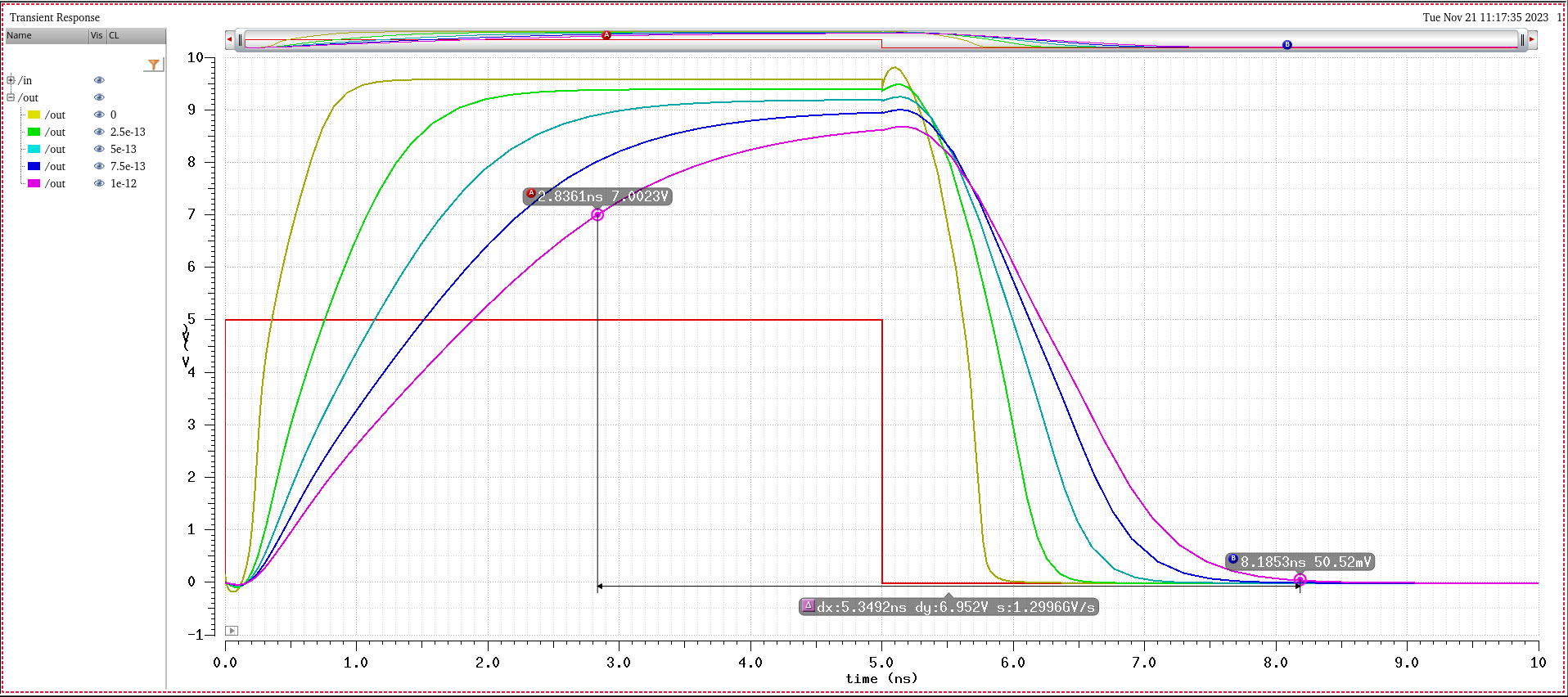
- For this test, VDD = 5.5V. As we can see below, with a maximum load of 1pF, the slowest rise
time to go above 7V was ~2.4ns and the slowest fall time was around
3.06ns. We also see that the output voltage goes well above 7V for a logic high and goes to near 0V for a logic low.
Part 2: Buffer Layout
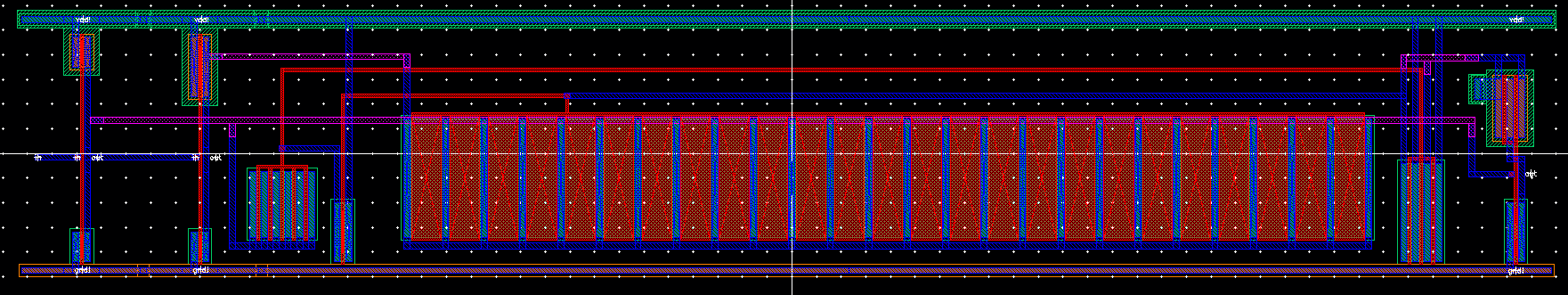
Layout:
Annotated View:
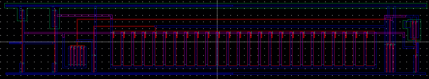
Extracted:
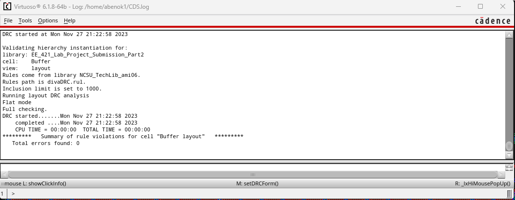
DRC:
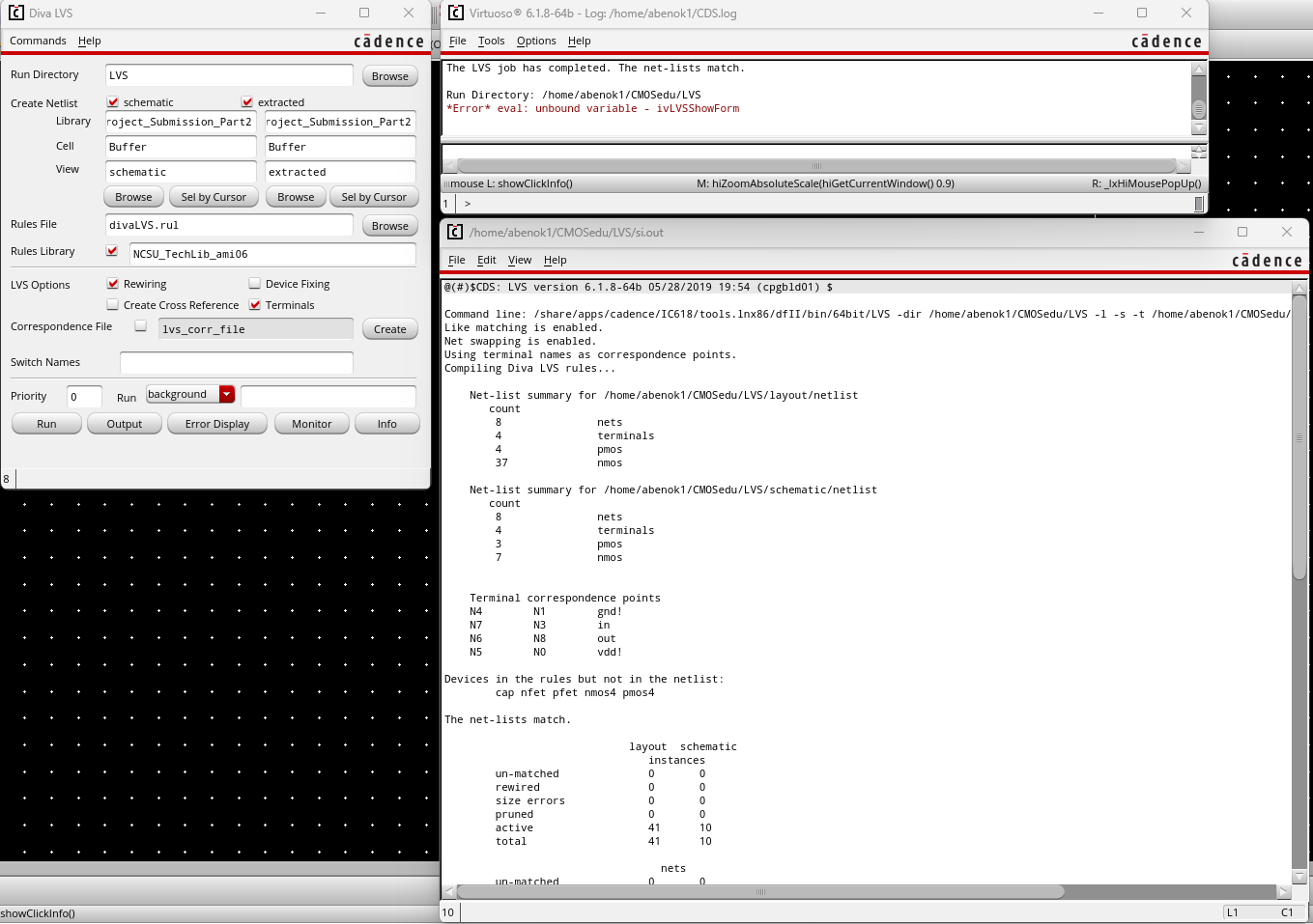
LVS:
Return to 421L Labs