Lab 7 - ECE 421L
Authored
by Kyle Abenojar, abenok1@unlv.nevada.edu
November 8th, 2023
Prelab:
For lab 7's prelab, we were tasked with completing Tutorial 5.
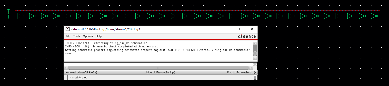
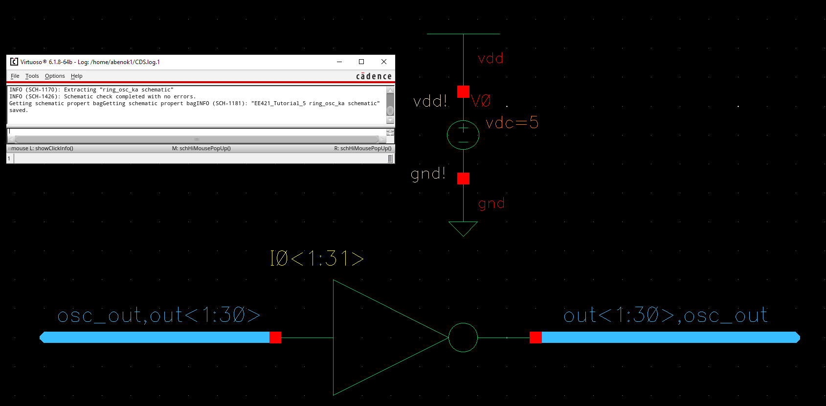
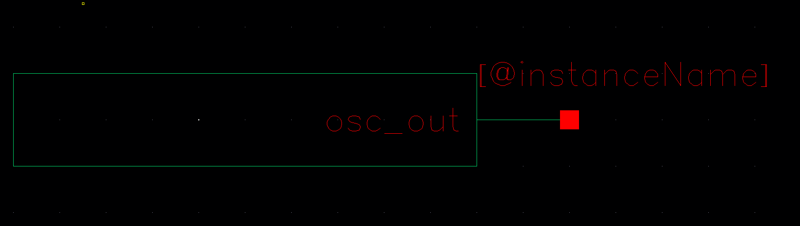
The
first step was create a ring oscillator. We accomplished this by using
31 inverters connected in a row with the input of the first inverter
tied to the output of the final inverter. Below was the schematic that
I generated.
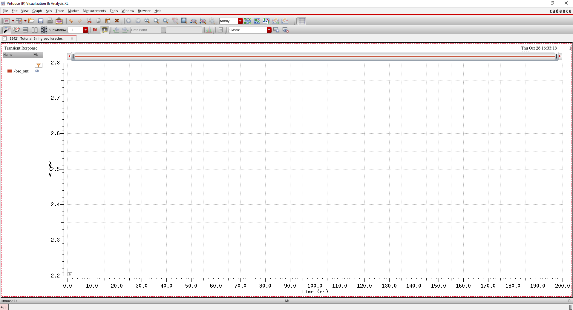
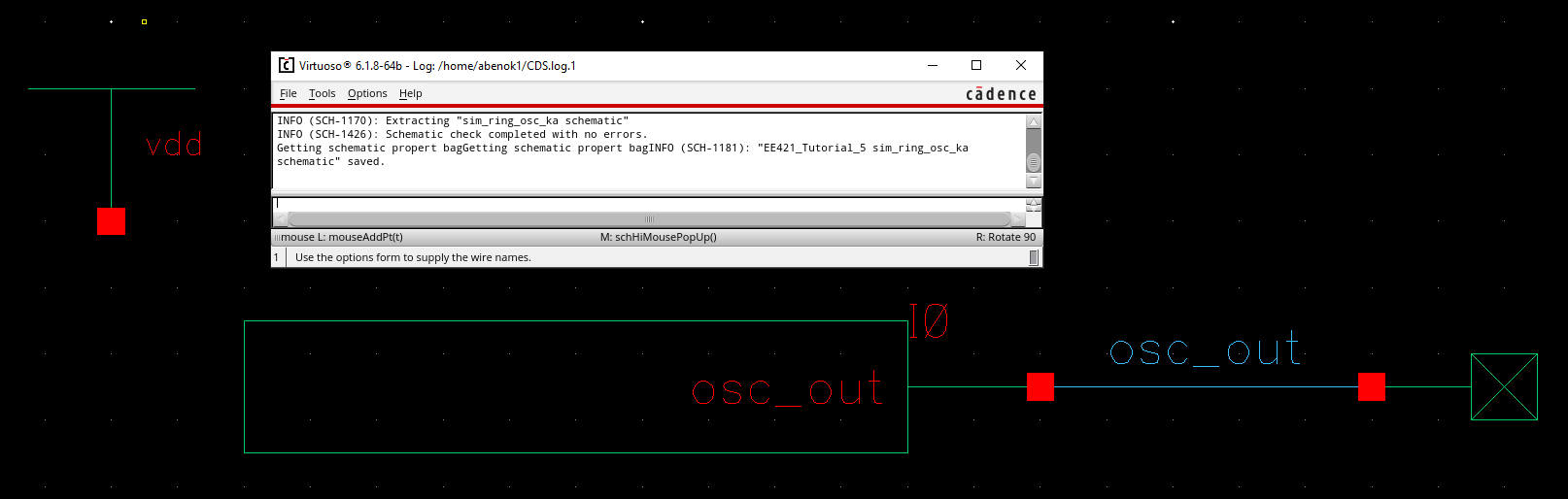
The
next step was to simulate our ring oscillator. I simulated my circuit
with a transient analysis for 200 ns. As seen below, the output stays
at 2.5V which is not what we expect. This is because we did not apply
an initial condition to our simulation.
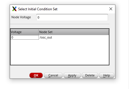
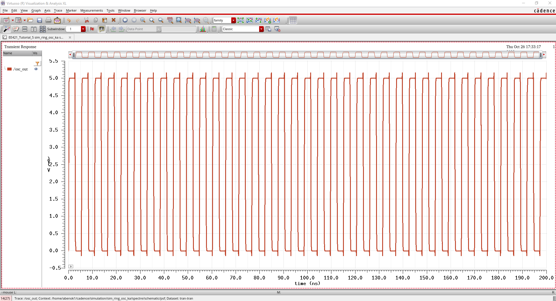
So, to fix this we apply an initial condition to our output and set it at 0V.
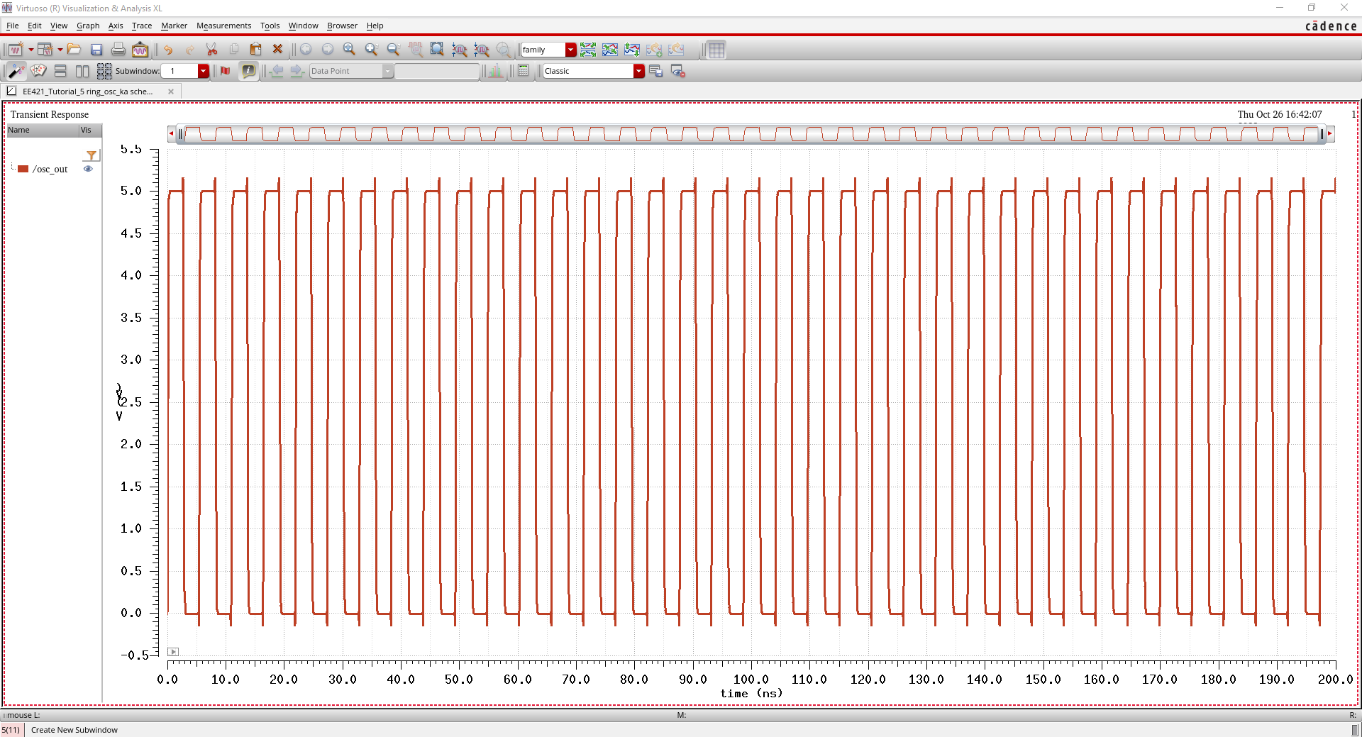
Now, when we simulate our circuit, we get oscillations from 0 to 5V as we expect.
Now,
we will learn how to use arrays to create a cleaner looking schematic.
We can have the same results by creating the following circuit.
And as expected, when we simulate the new schematic we get the same output as before.

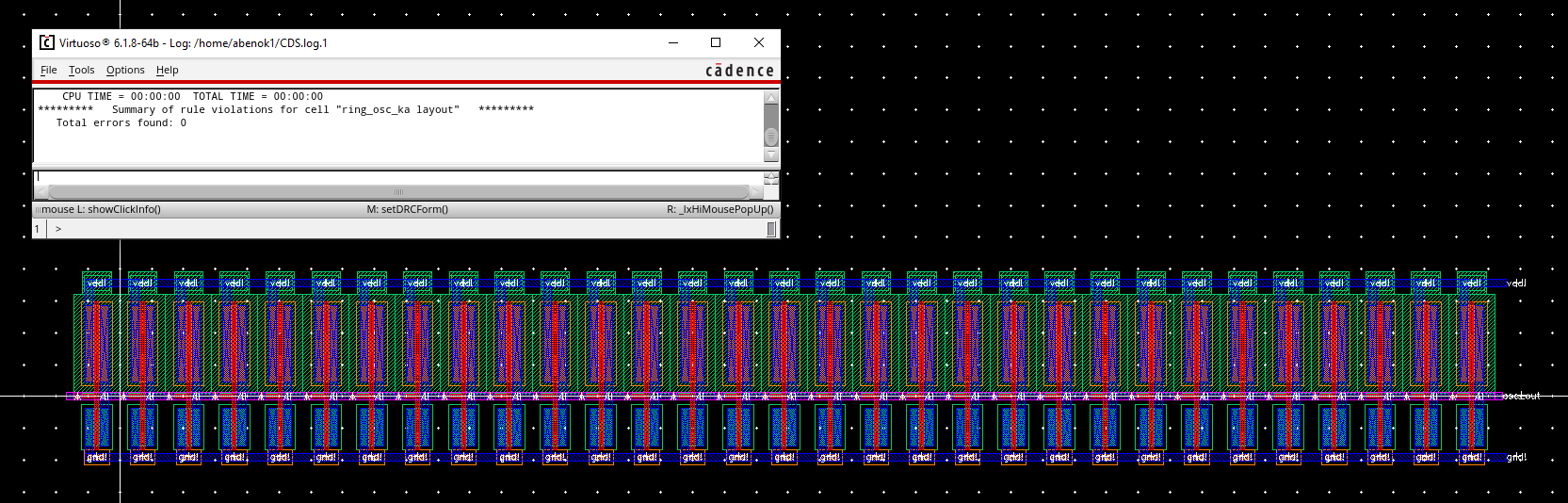
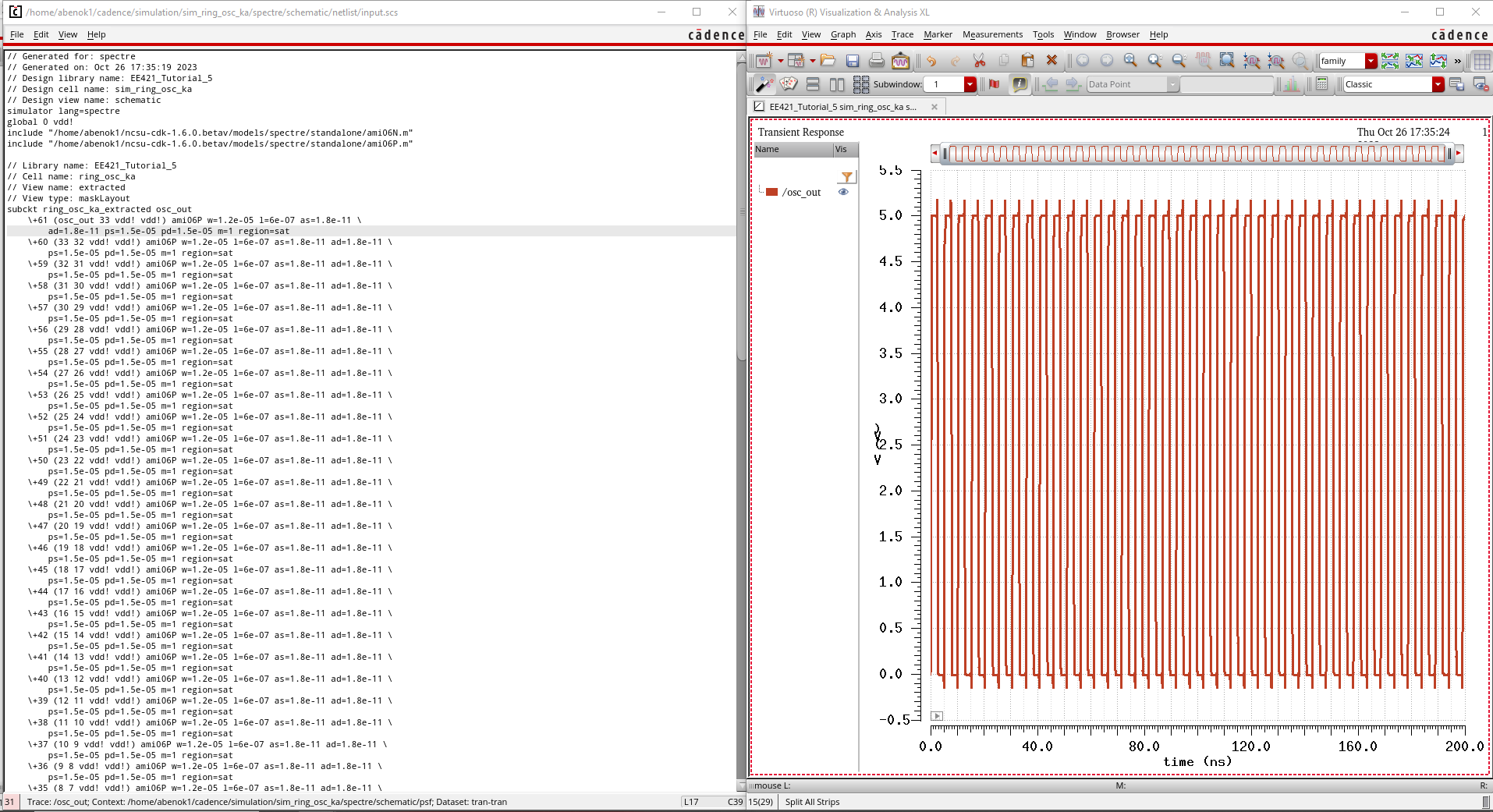
Next, we create a layout of our ring oscillator and perform a DRC to make sure our layout is clean..
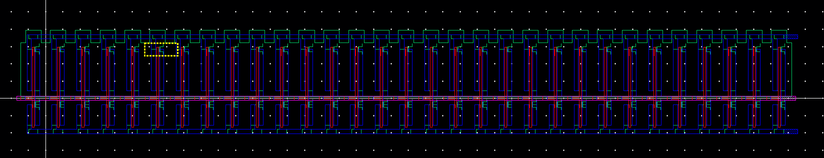
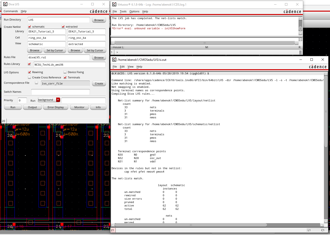
Then, we extract our layout and perform an LVS.
Next, we want to compare the operation of our schematic vs our layout so we go back and create a symbol for our ring oscillator.
We then created the following schematic to test our ring oscillator.
First we simulated the schematic of our ring oscillator and got the following.
Then, we tested the extracted schematic and got similar results.
Lab Report:
The
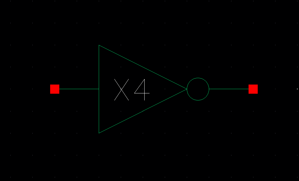
first step of the lab was to create a four bit inverter using arrays.
Below is my schematic and symbol for a four bit inverter.
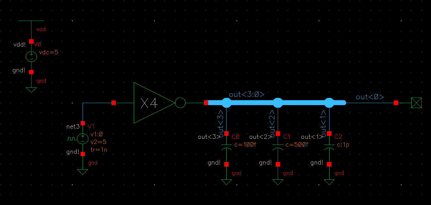
Next, I simulated the operation of my inverter with the following schematic.
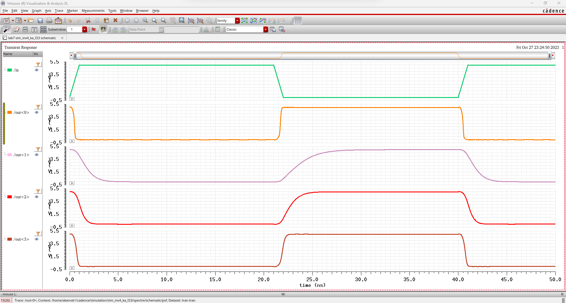
And
got the following output. As we can see, the larger the capacitive
load, the longer it takes for the output of the inverter to charge. 1pF
> 500 fF > 100fF, so as expected, it took out<1> the
longest amount of time to reach 5V with out<2> and out<3>
both getting faster with lighter loads. out<0> on the other hand
has no capacitive load so it switches to 5V the fastest.
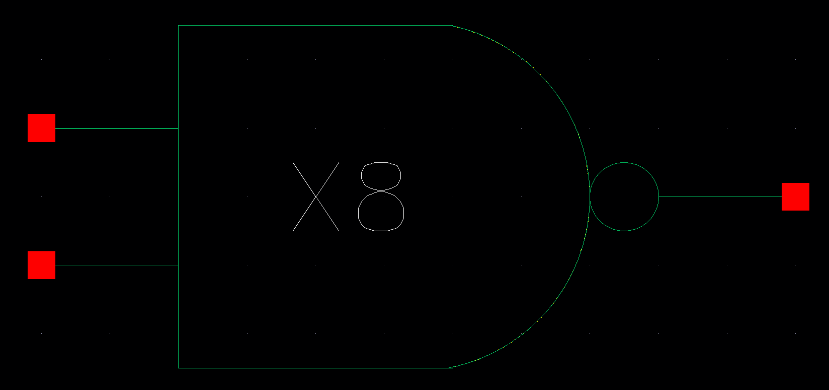
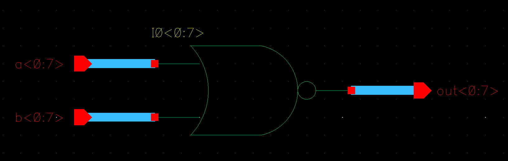
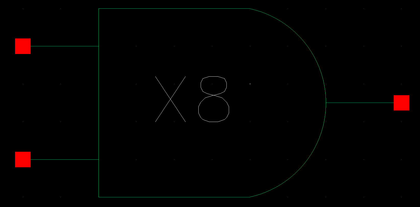
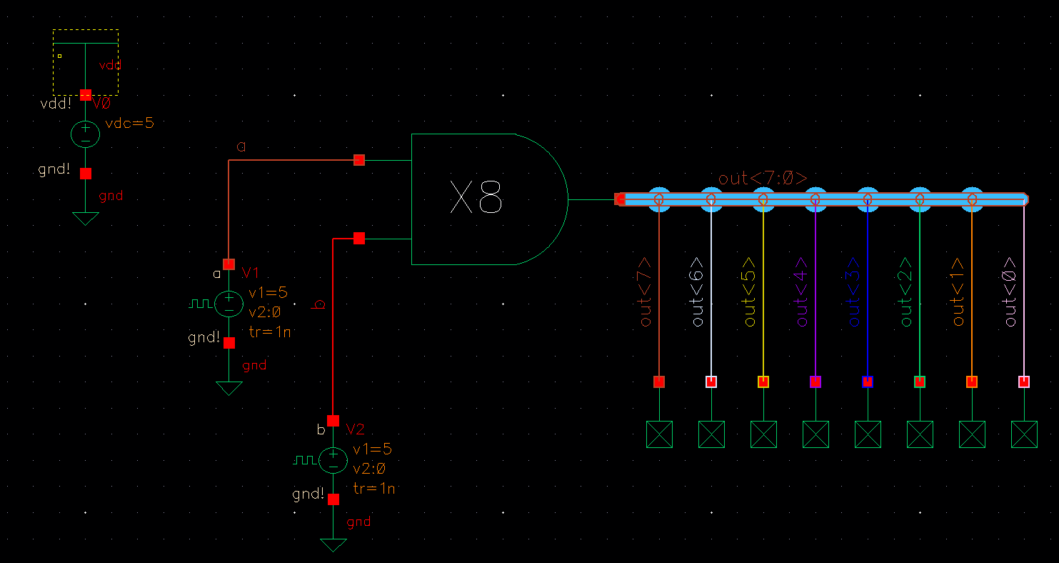
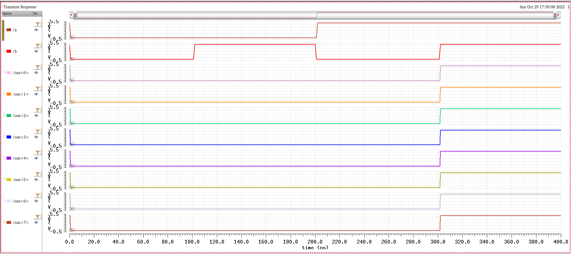
The next step was to create an 8-bit NAND gate. Below is my schematic and symbol for my 8-bit NAND.Pic

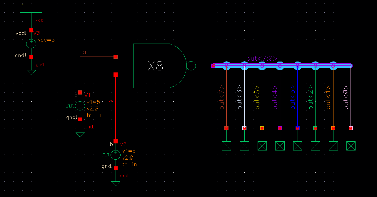
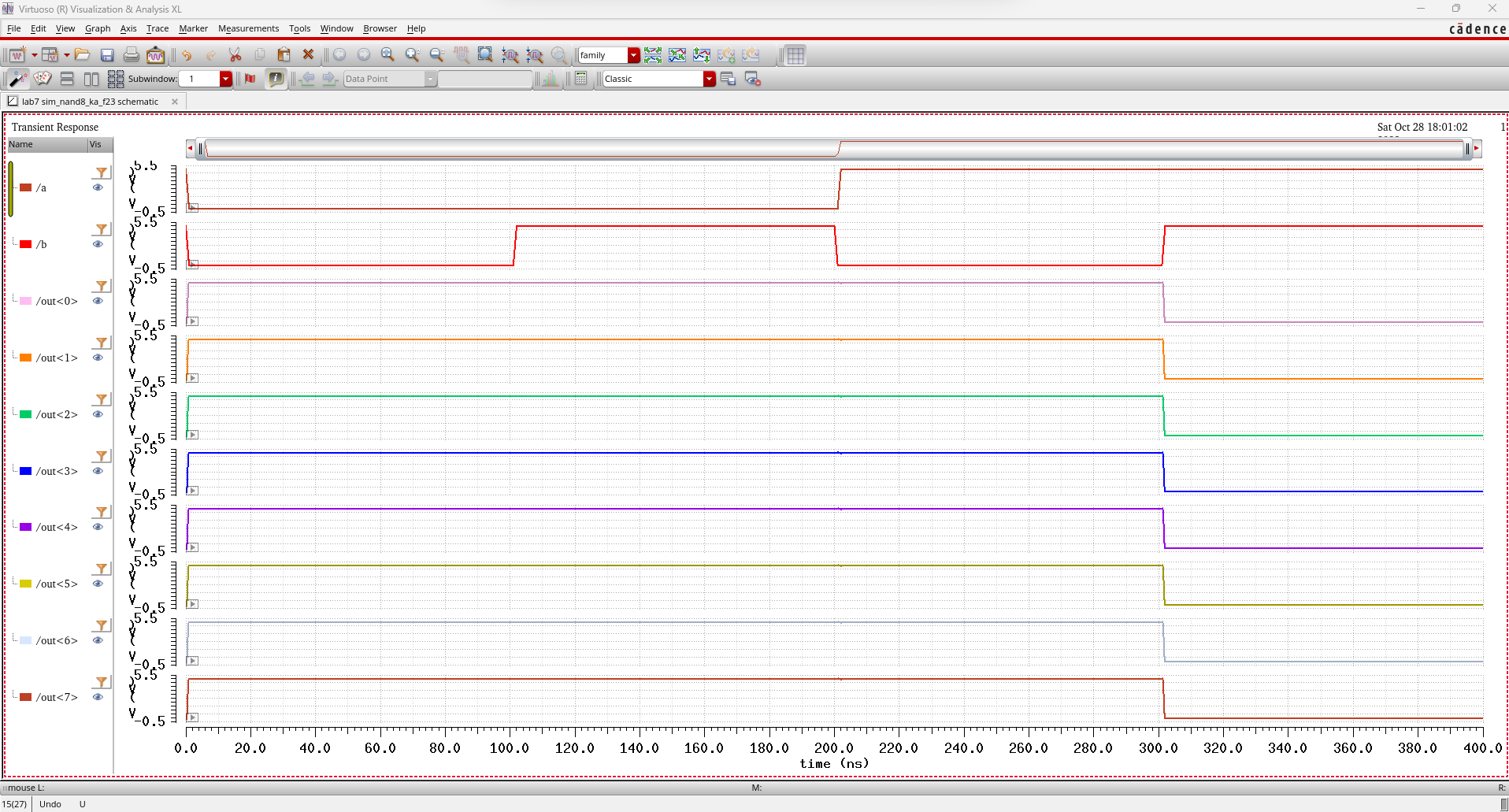
I
then tested my 8-bit NAND with the following schematic and got the
following output. As expected, with the same inputs and no load on each
output, we got the same output for each out bit. Each gate also had the
expected outputs for a NAND gate.
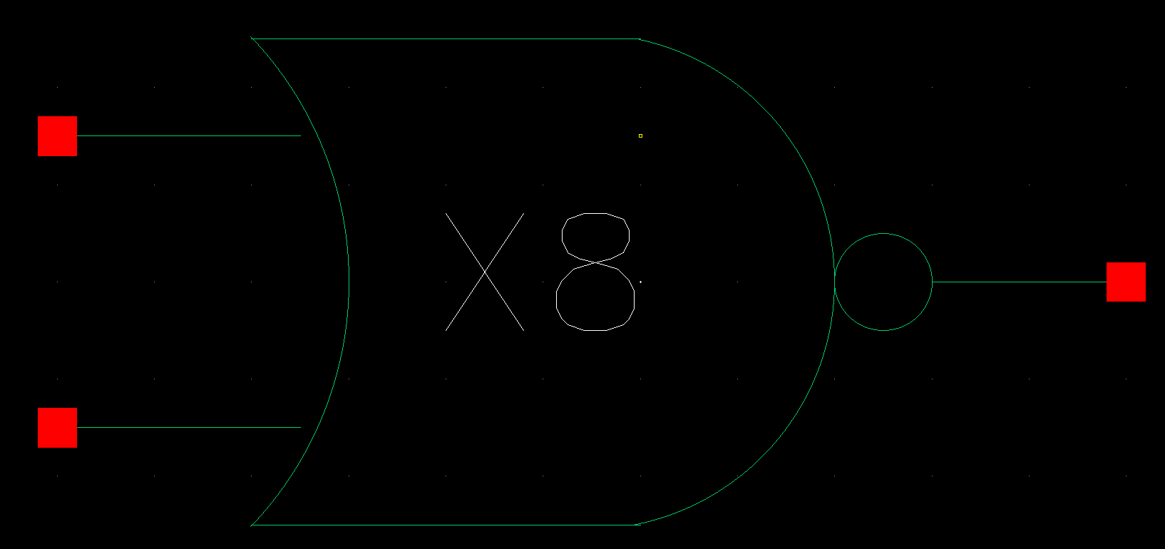
Next, I made the following schematic and symbol for an 8-bit NOR gate..
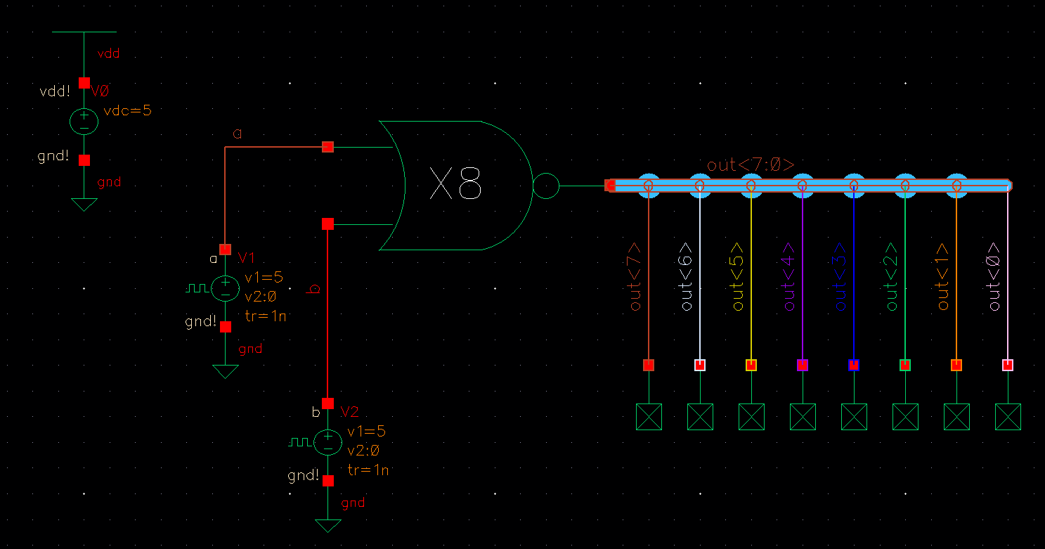
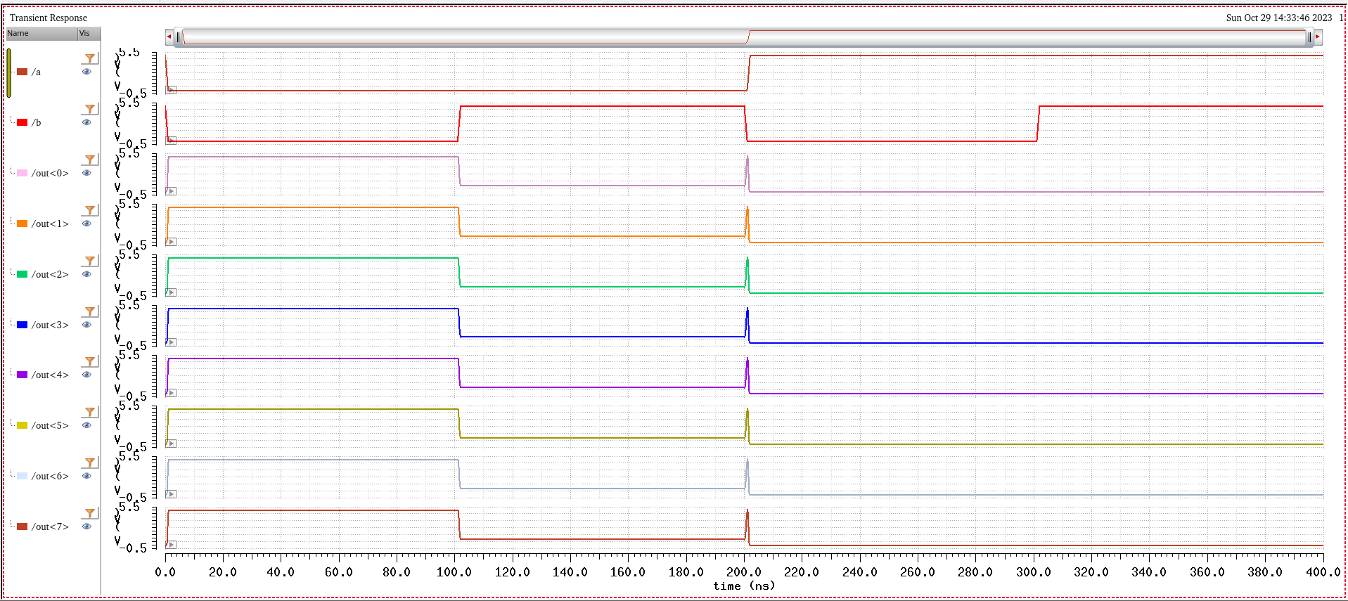
I then tested the operation of my 8-bit NOR gate with the following schematic and got the following output.
The
next gate I made was an 8-bit AND gate. I did this by connecting my
NAND gate's output to an inverter. Below are my schematic and symbol.
I then tested the operation of my 8-bit AND gate with the following schematic and got the following output.
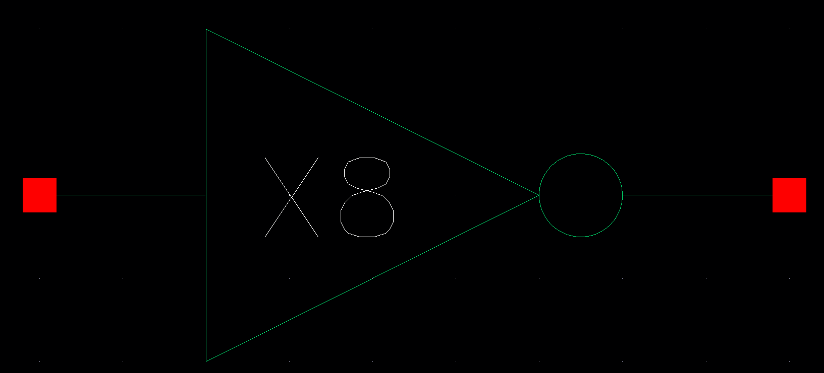
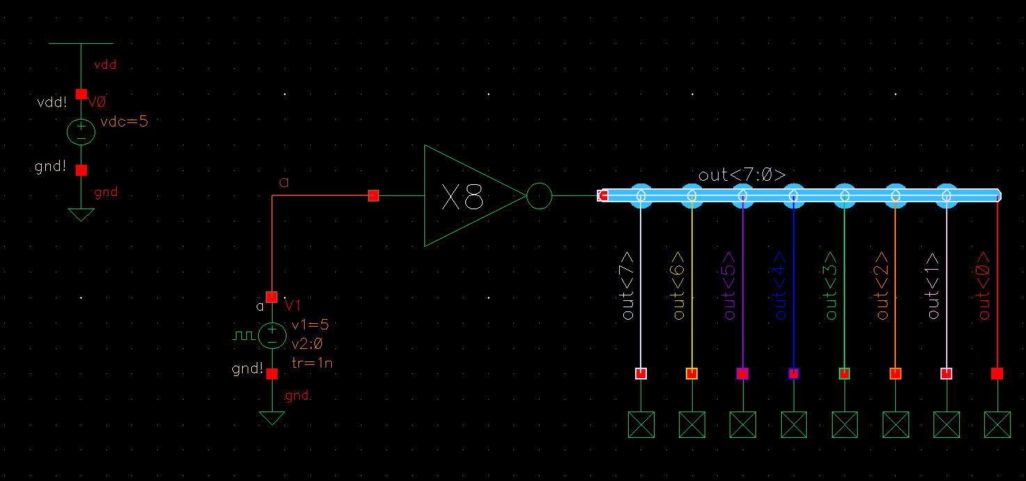
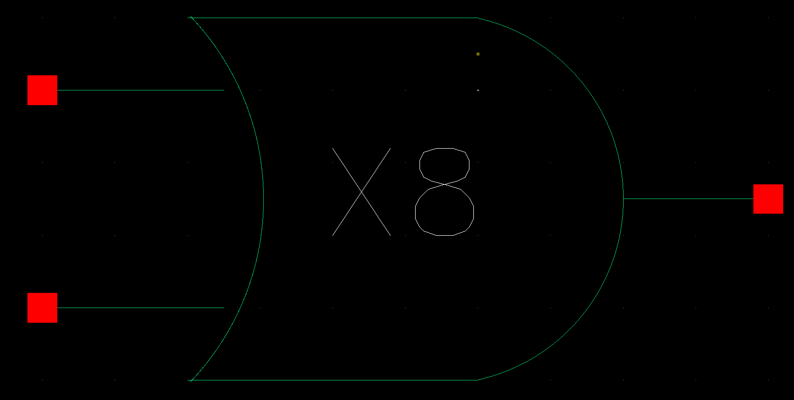
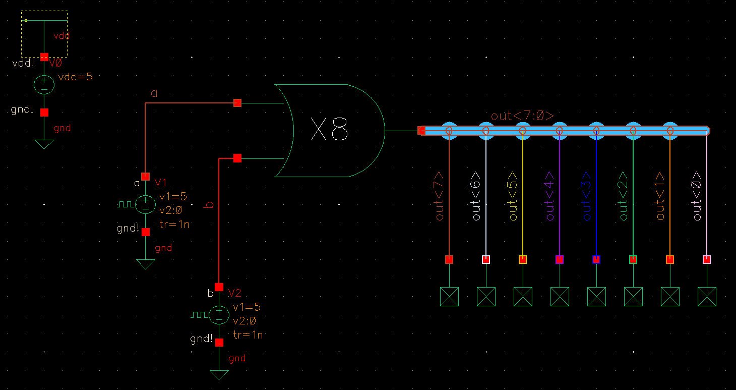
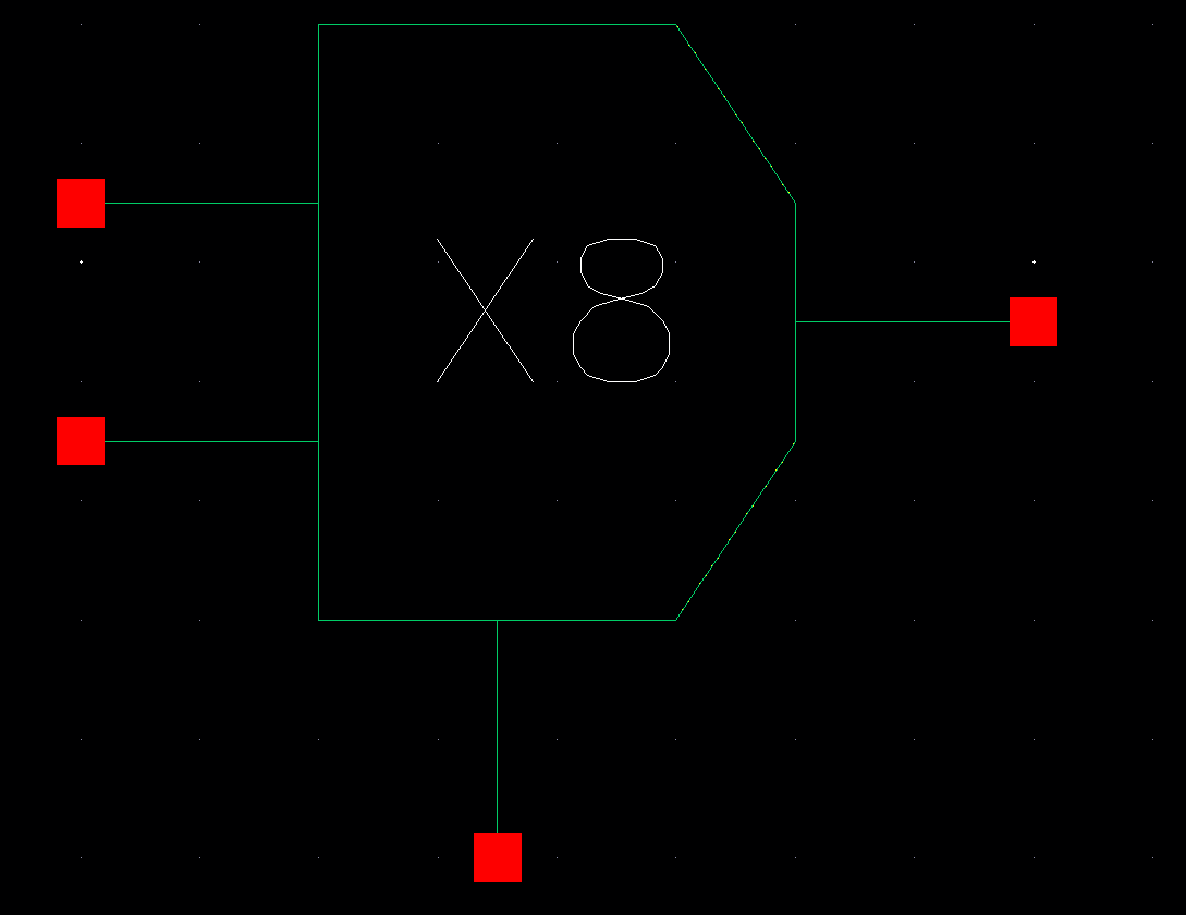
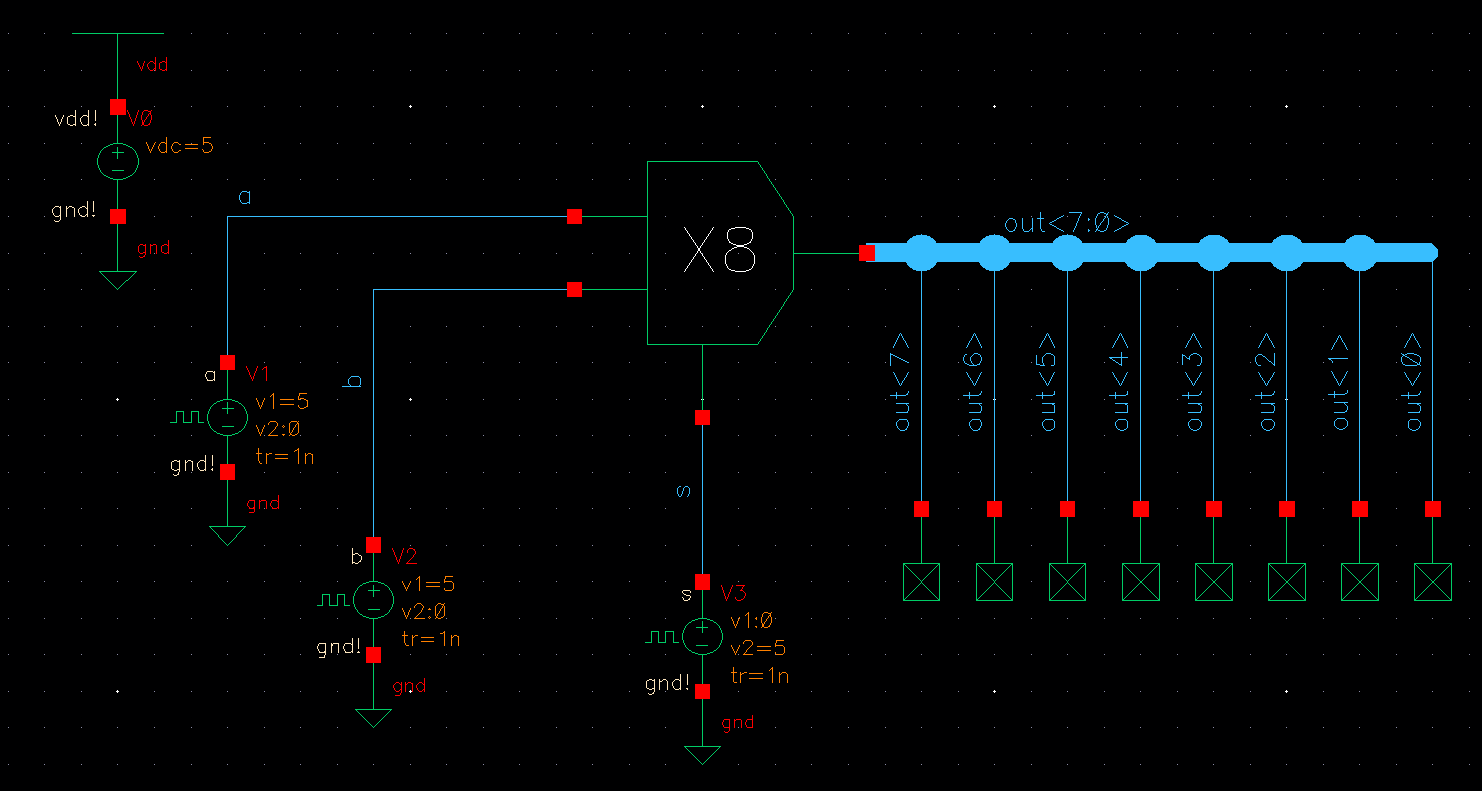
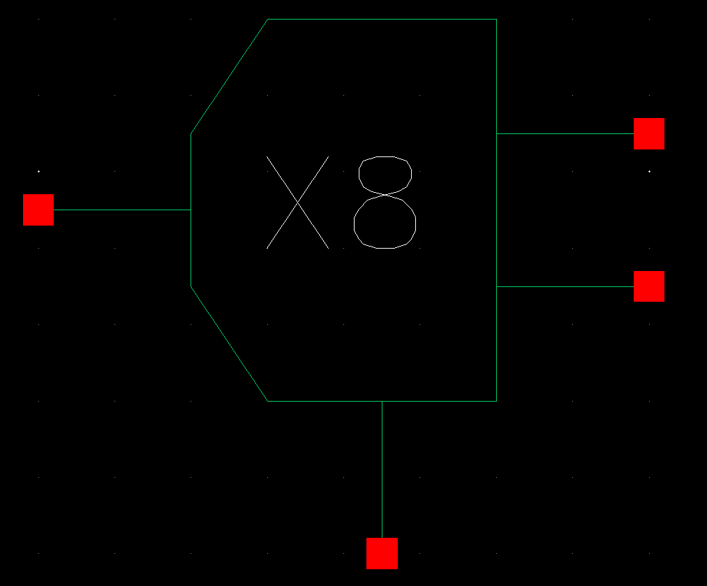
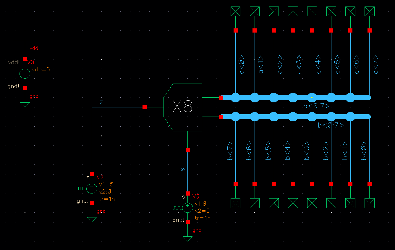
Next, I made the following schematic and symbol for an 8-bit inverter.
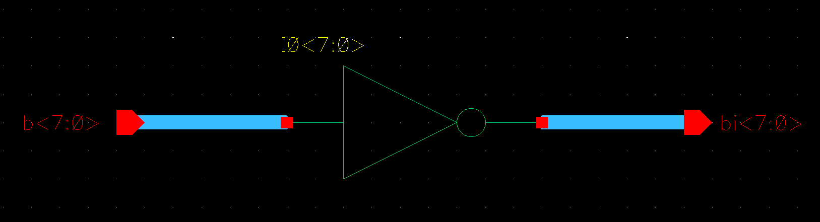
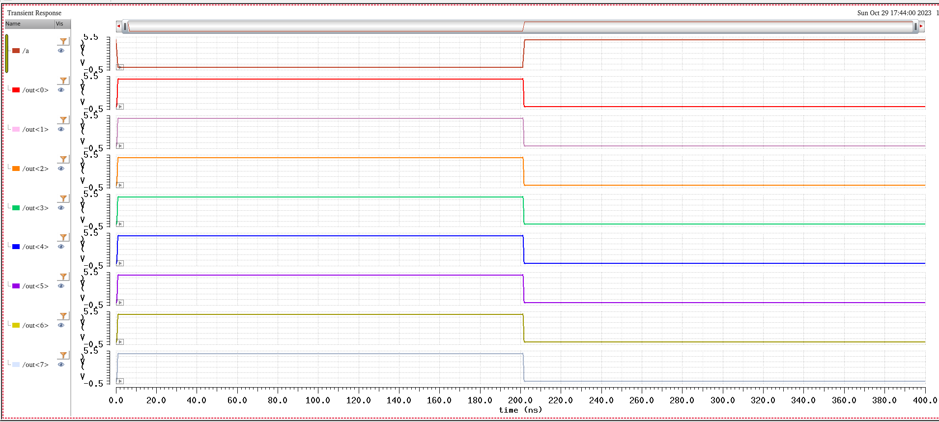
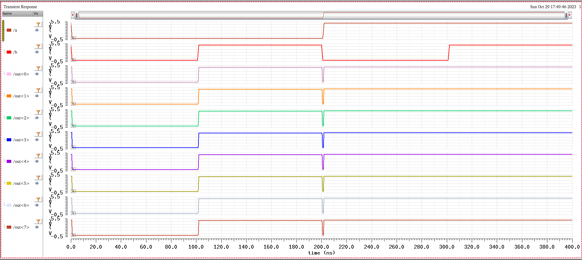
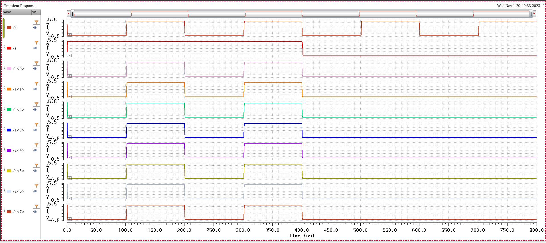
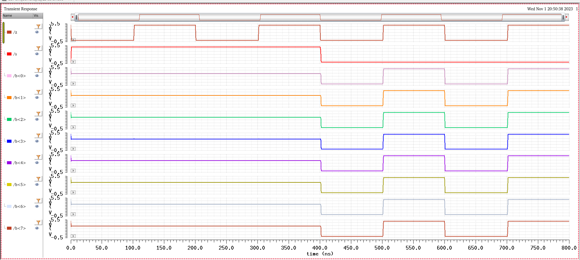
I then tested my 8-bit inverter's operation with the following schematic and got the following output.
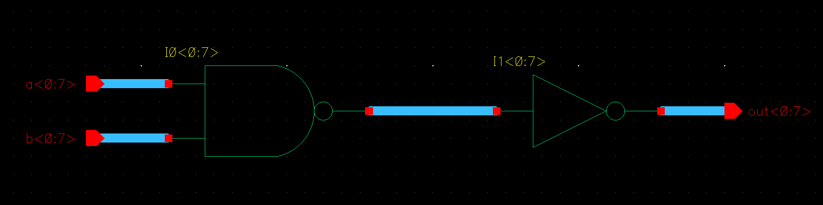
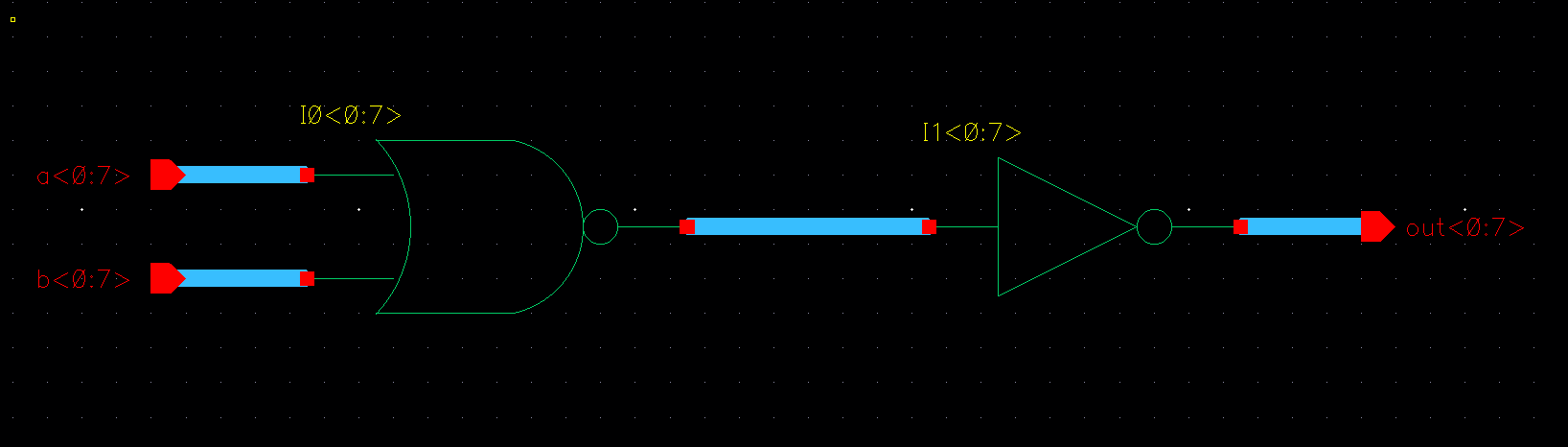
The
final gate I had to make was an 8-bit OR gate which I accomplished by
connecting my NOR gate's output to an inverter. Below are my schematic
and symbol.
I then tested the operation of my OR gate with the following schematic and got the following output.
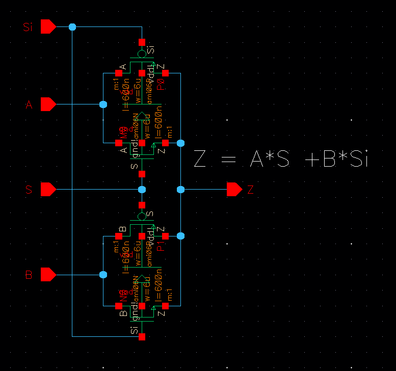
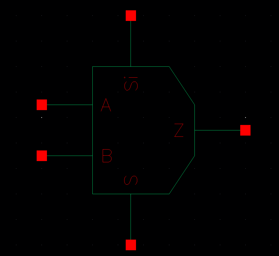
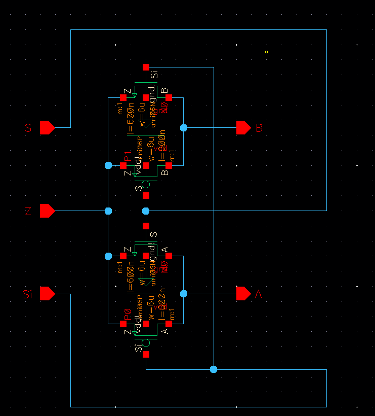
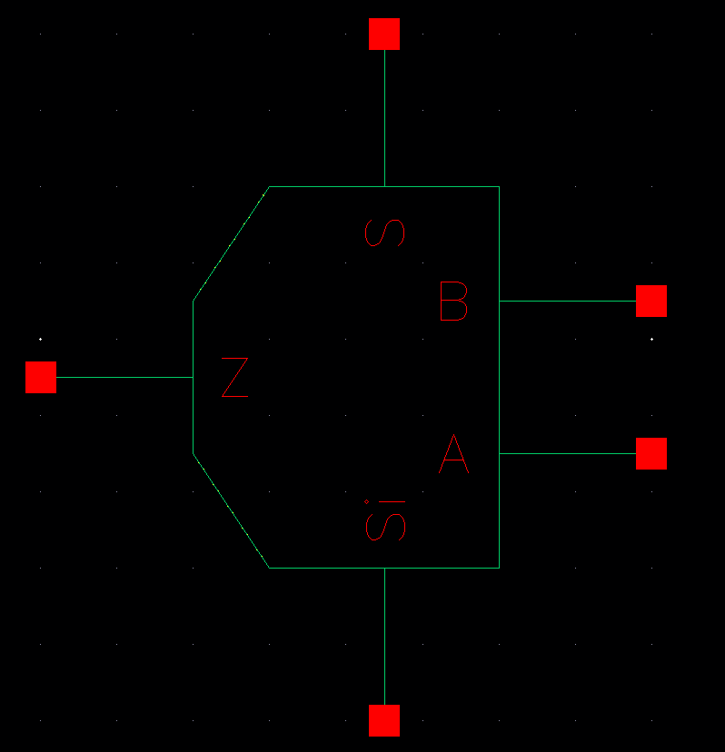
Next, we were given the following schematic of a 2 to 1 MUX. The way
this schematic works is that there is are four main inputs, A, B, S and
Si. S and its inversion, Si, act as the select line input. When the S
input is high, the input A is passed through to the output Z. When the
S input is low, the input B is passed through to the output Z.
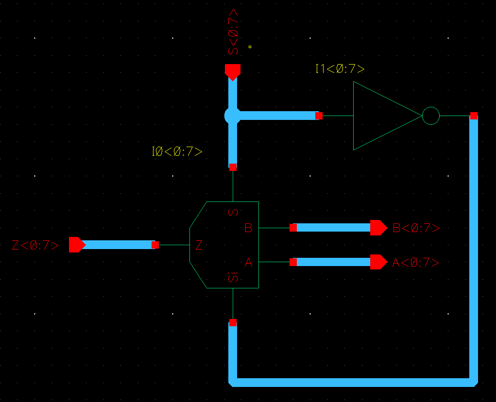
Using the given two to one mux, I made the following 8 bit wide two to
1 mux. An inverter was placed between the S input and Si so that the
design only requires the S input. Below are the schematic and symbol.
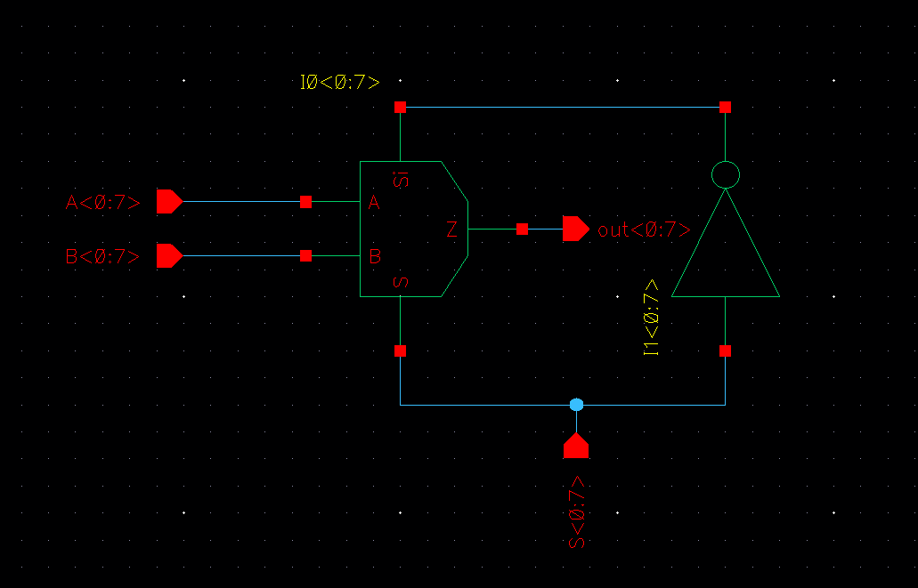
Next, I simulated the operation of my design with the following schematic and got the following output.
We can use the same schematic to create a two to one DEMUX by flipping
the inputs into outputs and the outputs into input as shown below. Now,
we are passing the Z signal input and outputting it either to A if S is
high or B if S is low.
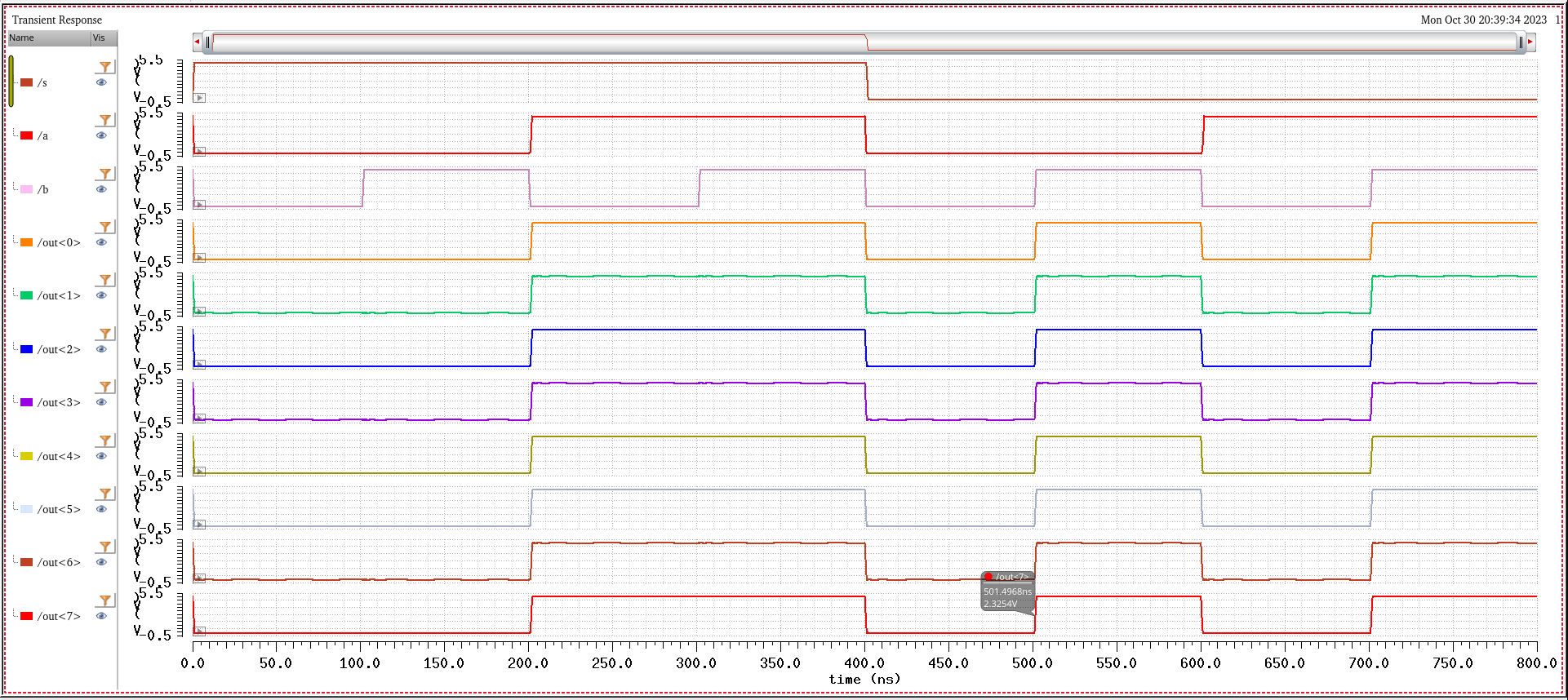
Once again, I made an 8 bit wide two to one DEMUX similar to the MUX with an inverter between S and Si.
I then tested the operation of my DEMUX with the following schematic and got the following output.
Output for A, the input Z is passed to A when S is high
Output for B, the input Z is passed to B when S is low
For the next part of the lab, I created a full adder using the
And-Or-Invert (AOI) schematic. Figure 12.20 from the book was
referenced to create the following schematic.
I then used this as the building block to create an 8 bit adder. Below are the schematic and symbol.
Next, I tested the operation of my 8-bit adder with the following schematic and got the following output.

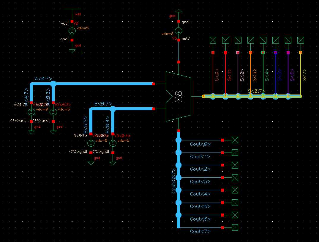
The
S output is the total sum of the inputs A<0:7>, B<0:7> and
Cin. In the simulation, A = 0000_1111, B = 0001_1111, and Cin = 1.
Adding these together, we should get S = 0010_1111 which is what we get
as seen below.
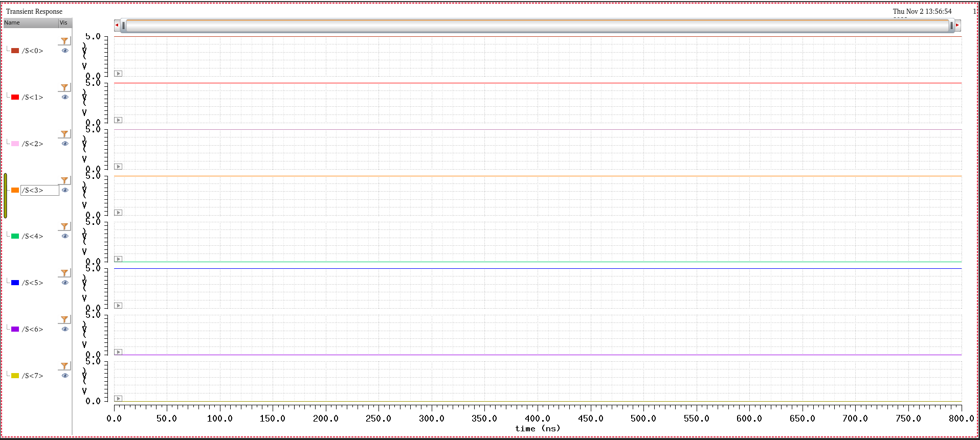
The
outputs Cout<0:7> are the carryouts of each full adder.
Cout<0> is the carryout of the first adder, Cout<1> is the
carryout of the second adder, and so on.
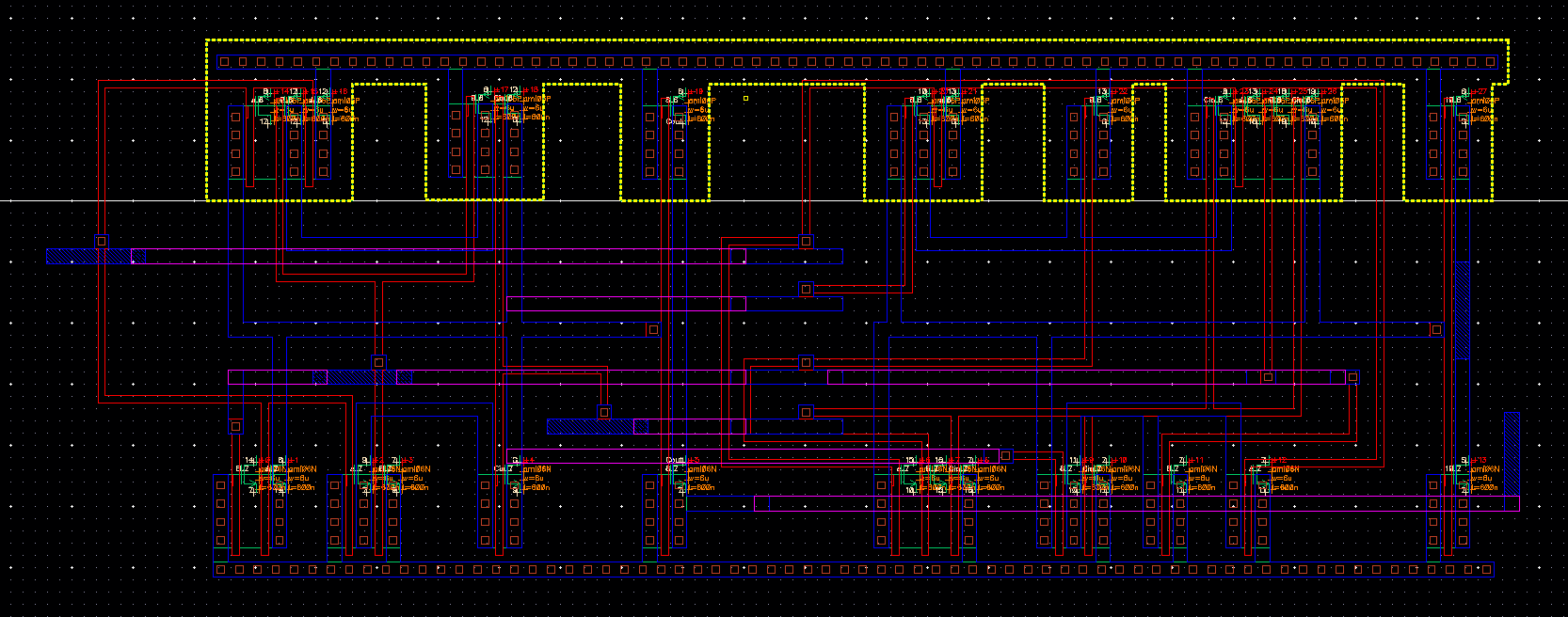
The
final step of the lab was to generate a layout for our 8 bit full
adder. To do this, I first made the layout for an individual AOI Full
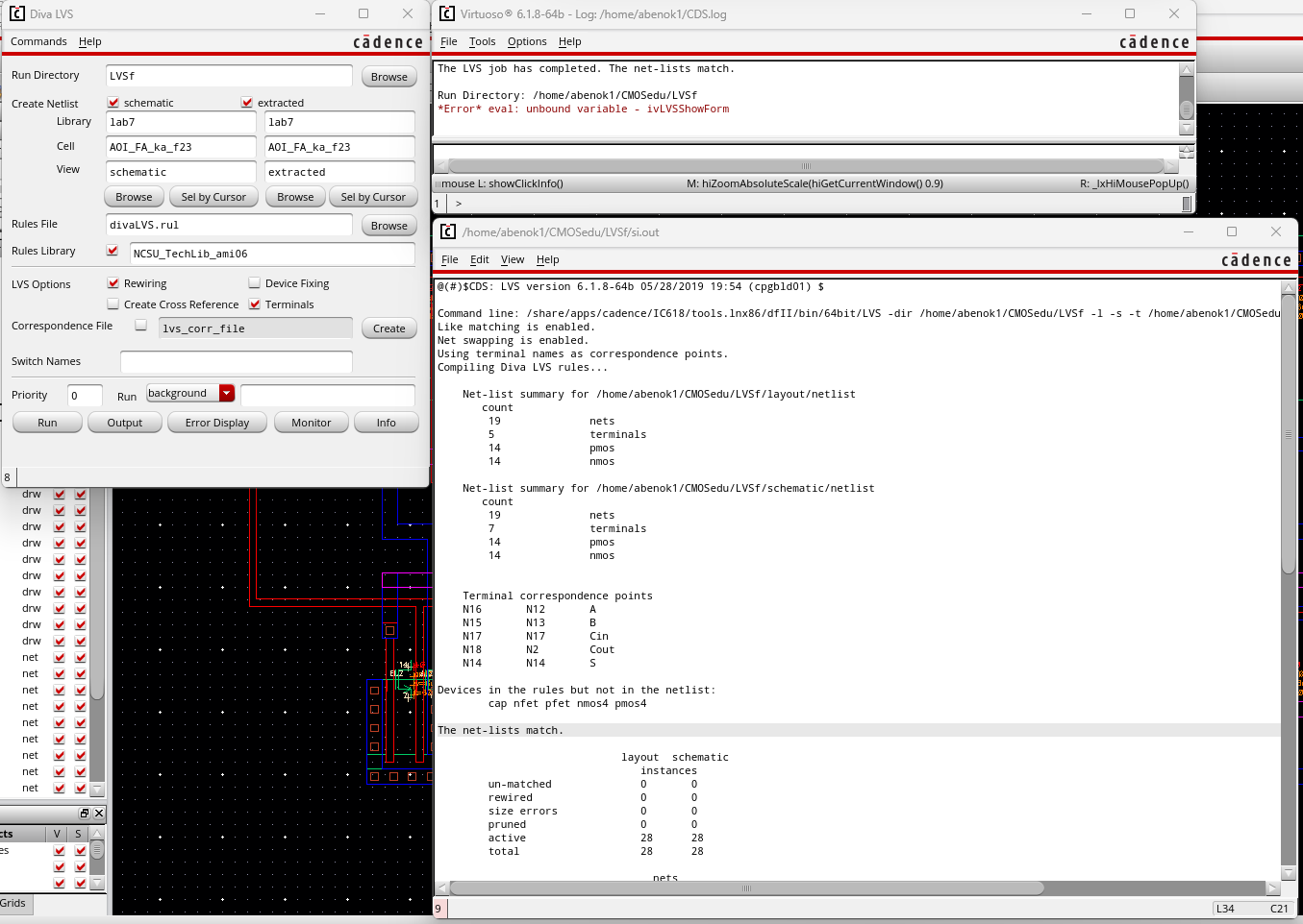
Adder and ensured that it DRC'ed and LVS'ed.
Full Adder Layout:
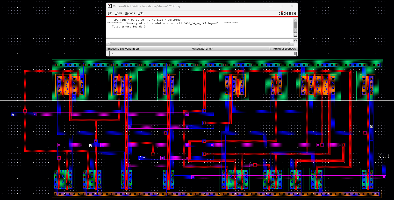
Full Adder Extracted View and LVS:
Once
this was done, I was able to start working the 8-bit adder. First, I
put two full adder layouts together and connected the Cout of the first
adder to the Cin of the second adder.
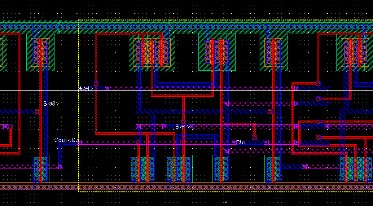
After
that, I was able to use the copy tool to create 8 copies of the full
adder layout. Then I added the proper input and output pins (input:
Cin, A<0:7>, B<0:7>; output: Cout<0:7> S<0:7>)
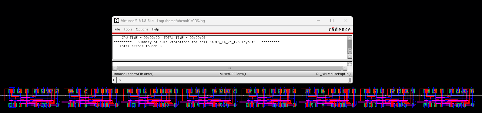
on metal 1. Once this was done I ensured that my layout DRC'ed and
LVS'ed cleanly.
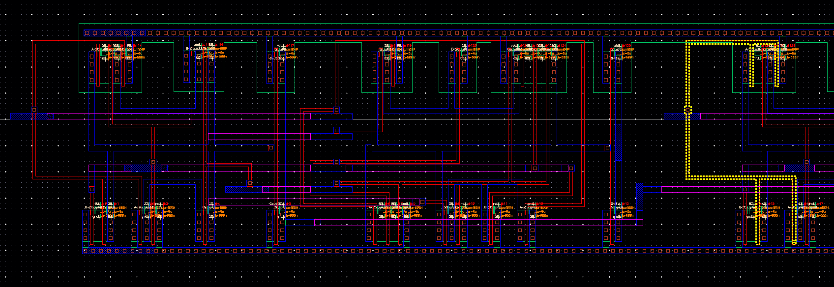
Full view of 8-bit Full Adder Layout:
Partial Extracted view of 8-bit Full Adder:
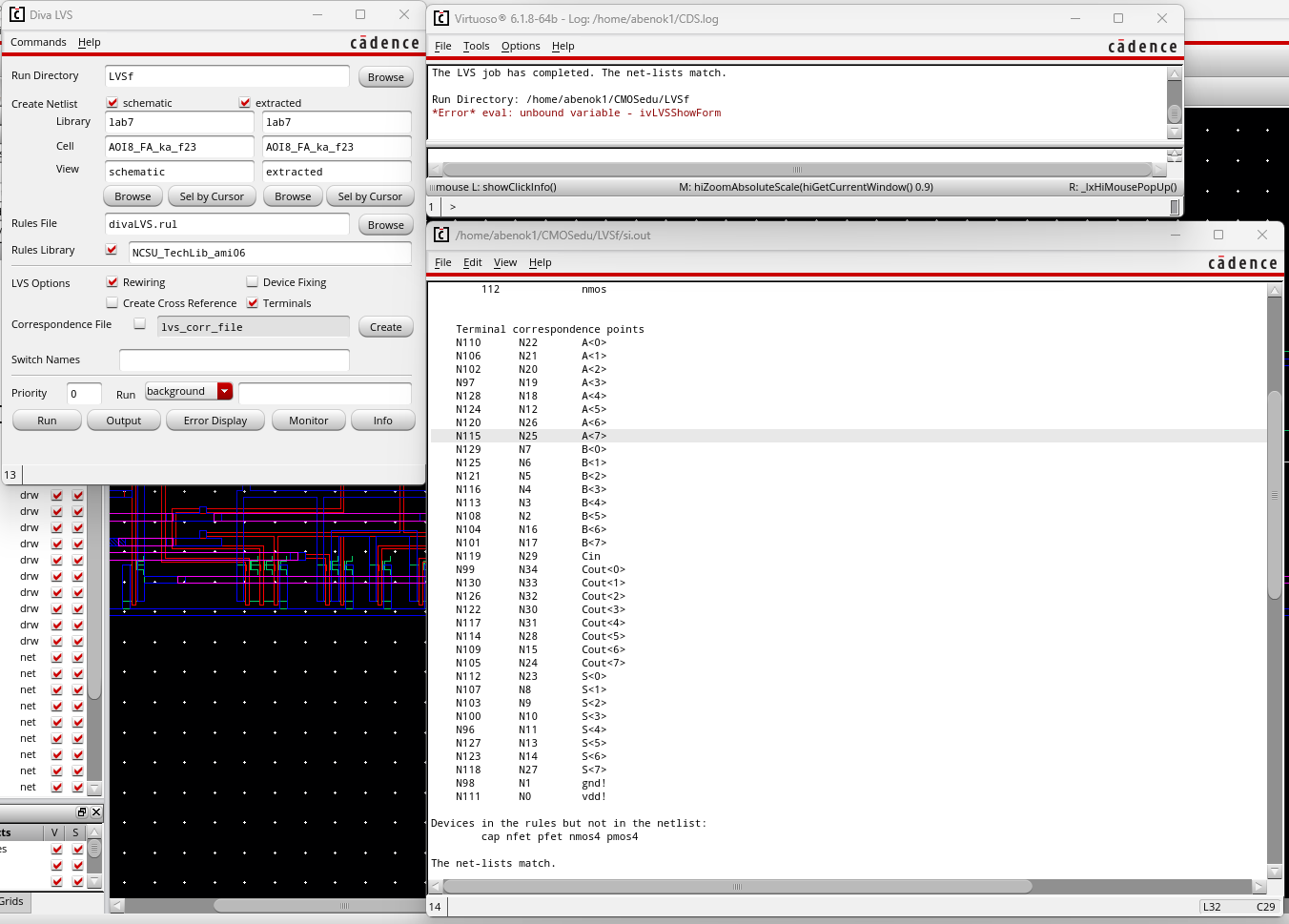
Full view of 8-bit Full Adder and LVS:


Return to 421L Labs