Lab 6 - ECE 421L
Authored
by Kyle Abenojar, abenok1@unlv.nevada.edu
October 25th, 2023
Prelab:
For lab 6, we were tasked with finishing Tutorial 4.
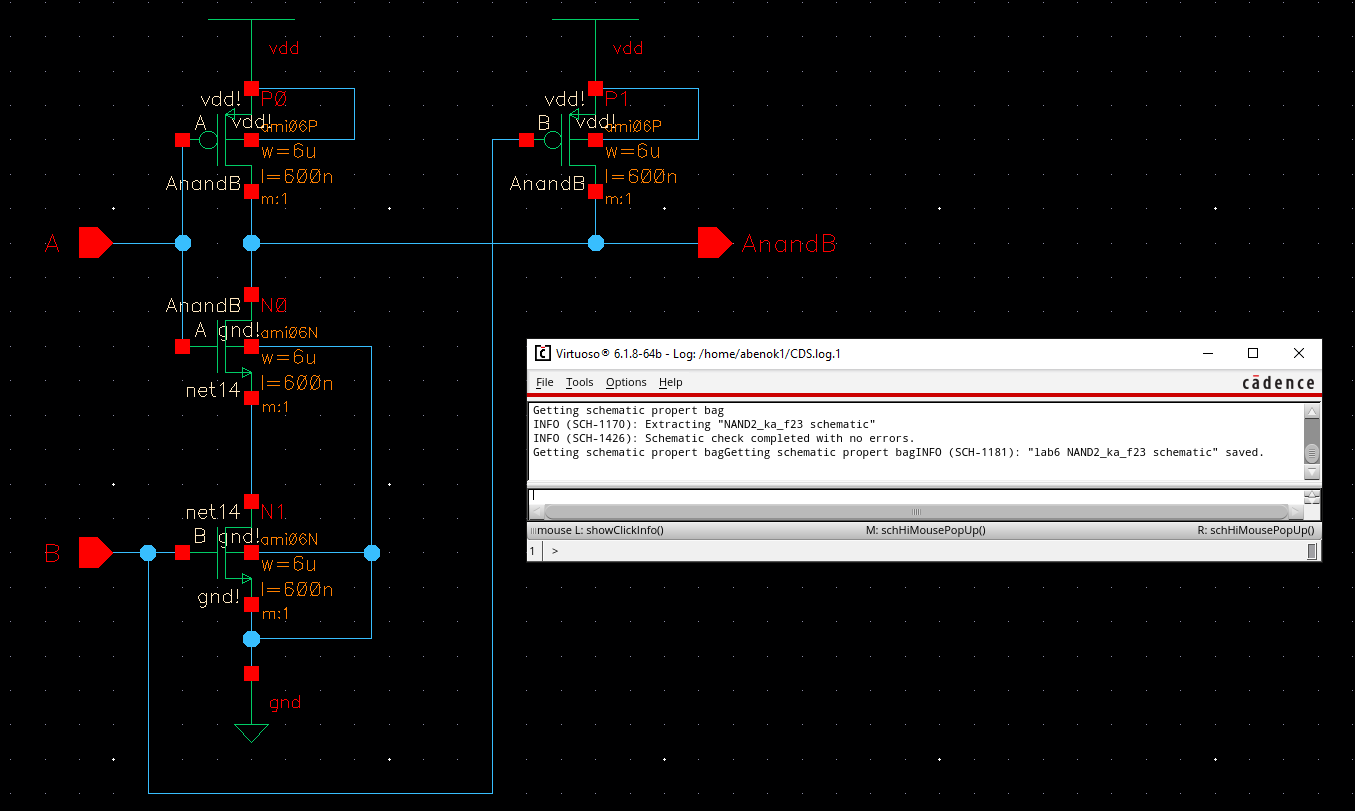
The first step was to create the schematic for a NAND gate.
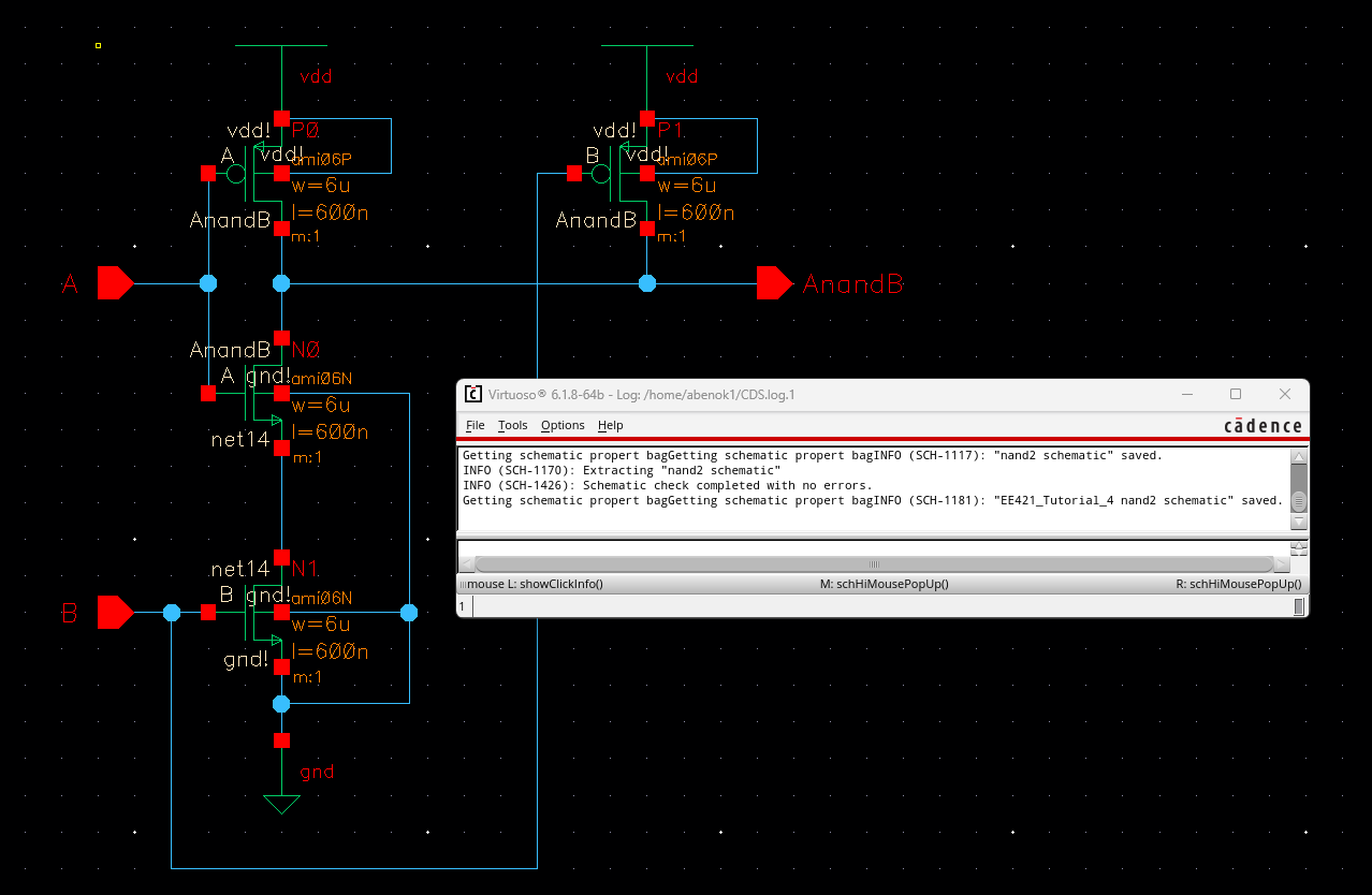
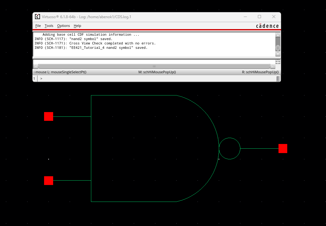
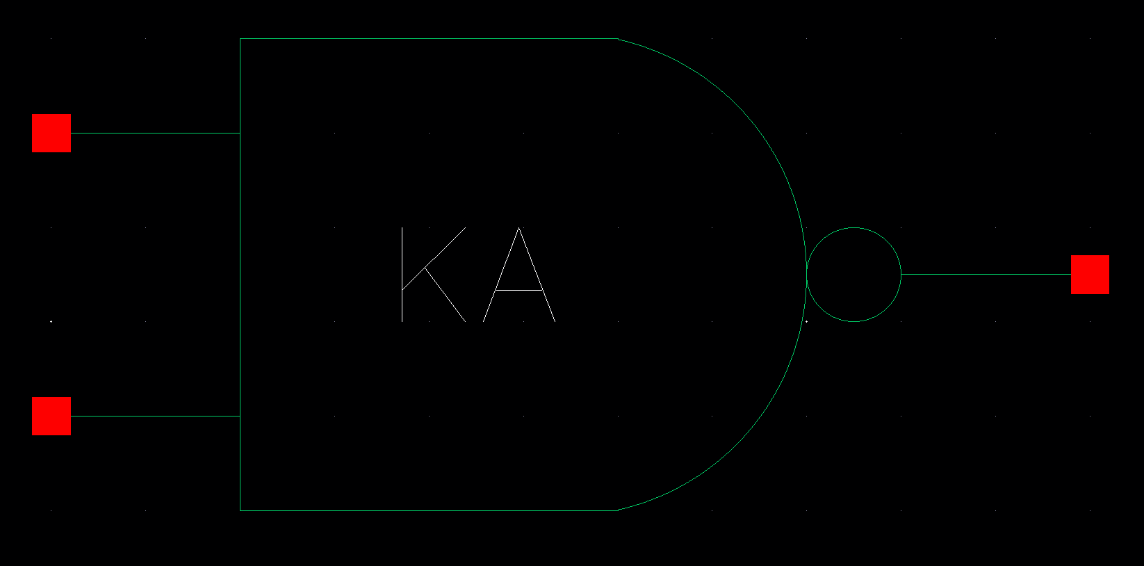
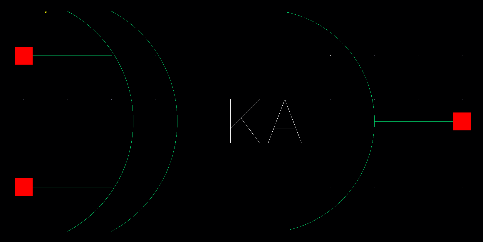
Next, we made a symbol using the typical symbol of a NAND gate.
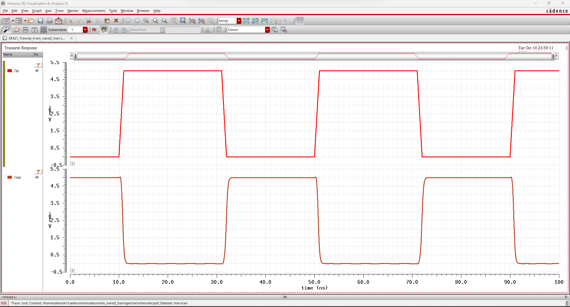
Then we tested the operation of our circuit and got the following.
After
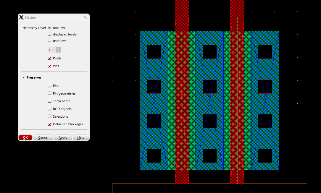
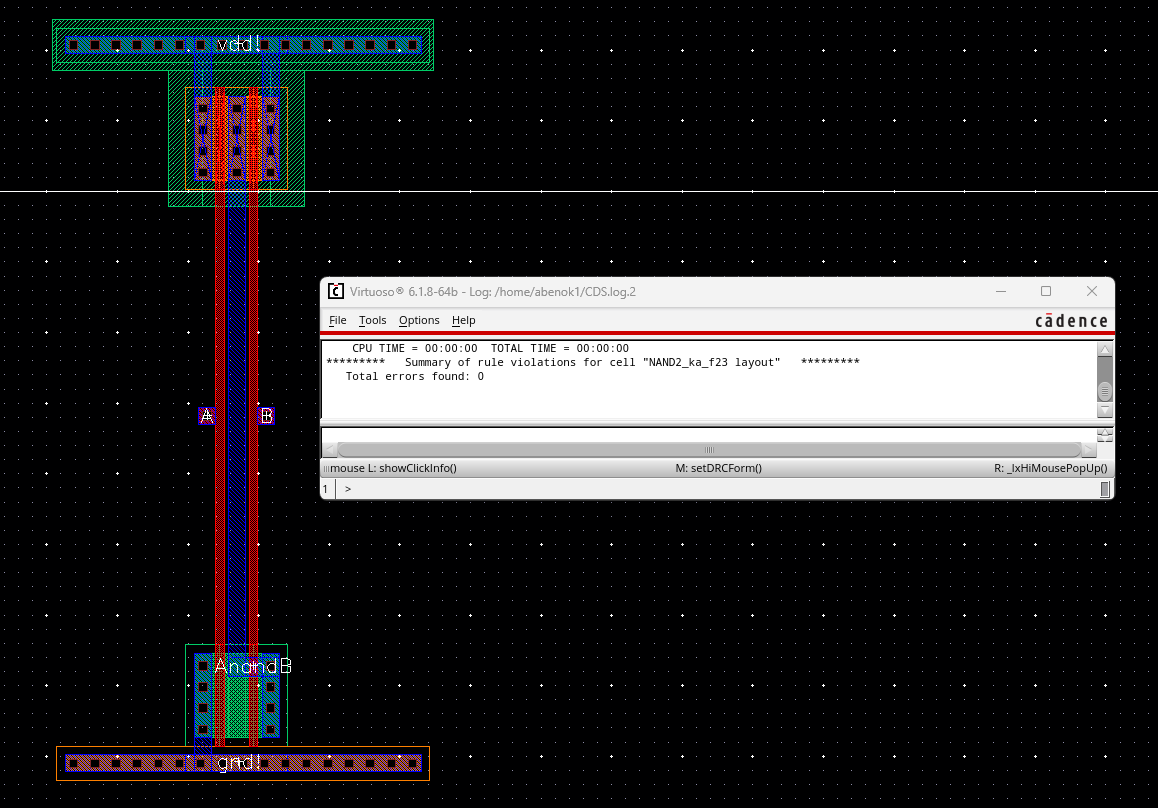
testing its operation, we built the layout for our NAND gate. One of
the new tools we used was the flatten tool. This takes our instance and
"flattens" as if it were rectangles we drew on our layout.
With that, we were able to make the layout for our NAND gate.
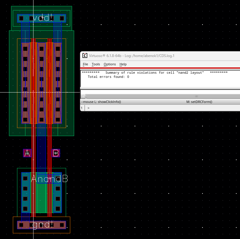
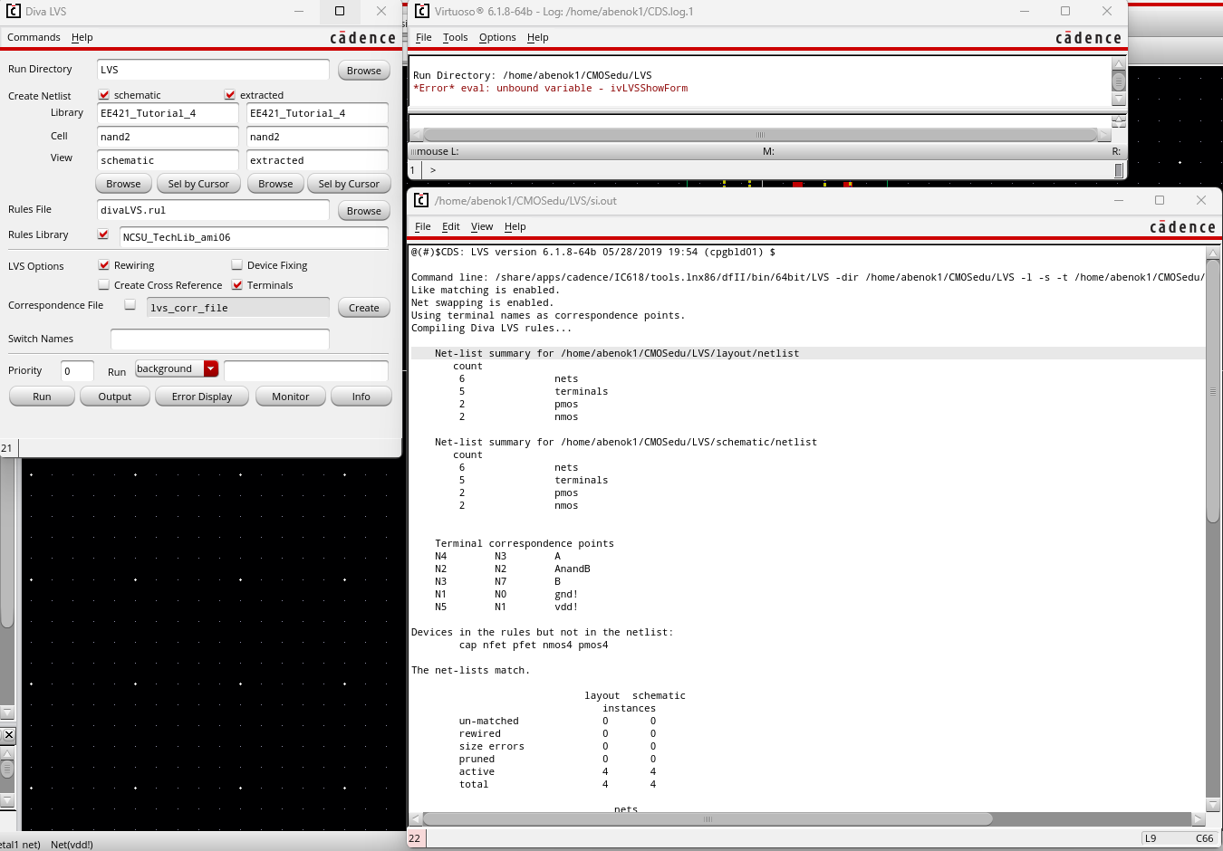
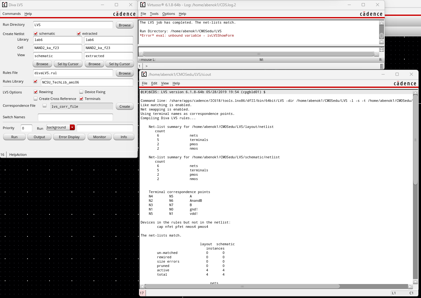
We then extracted our layout and performed an LVS.
Lab Report:
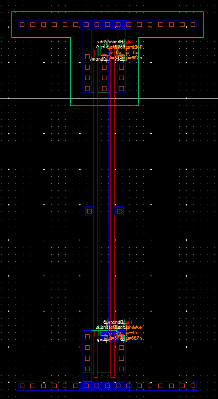
To
start, we needed to make the schematic, symbol, and layout as well as
LVS the extracted view of a NAND gate using 6u/0.6u MOSFETS. Slightly
modifying the NAND gate made in tutorial 4, I got the following. 1)
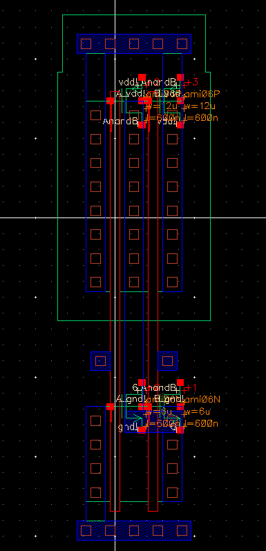
NAND schematic, 2) NAND symbol, 3) NAND layout, 4) NAND extracted view,
5) LVS results
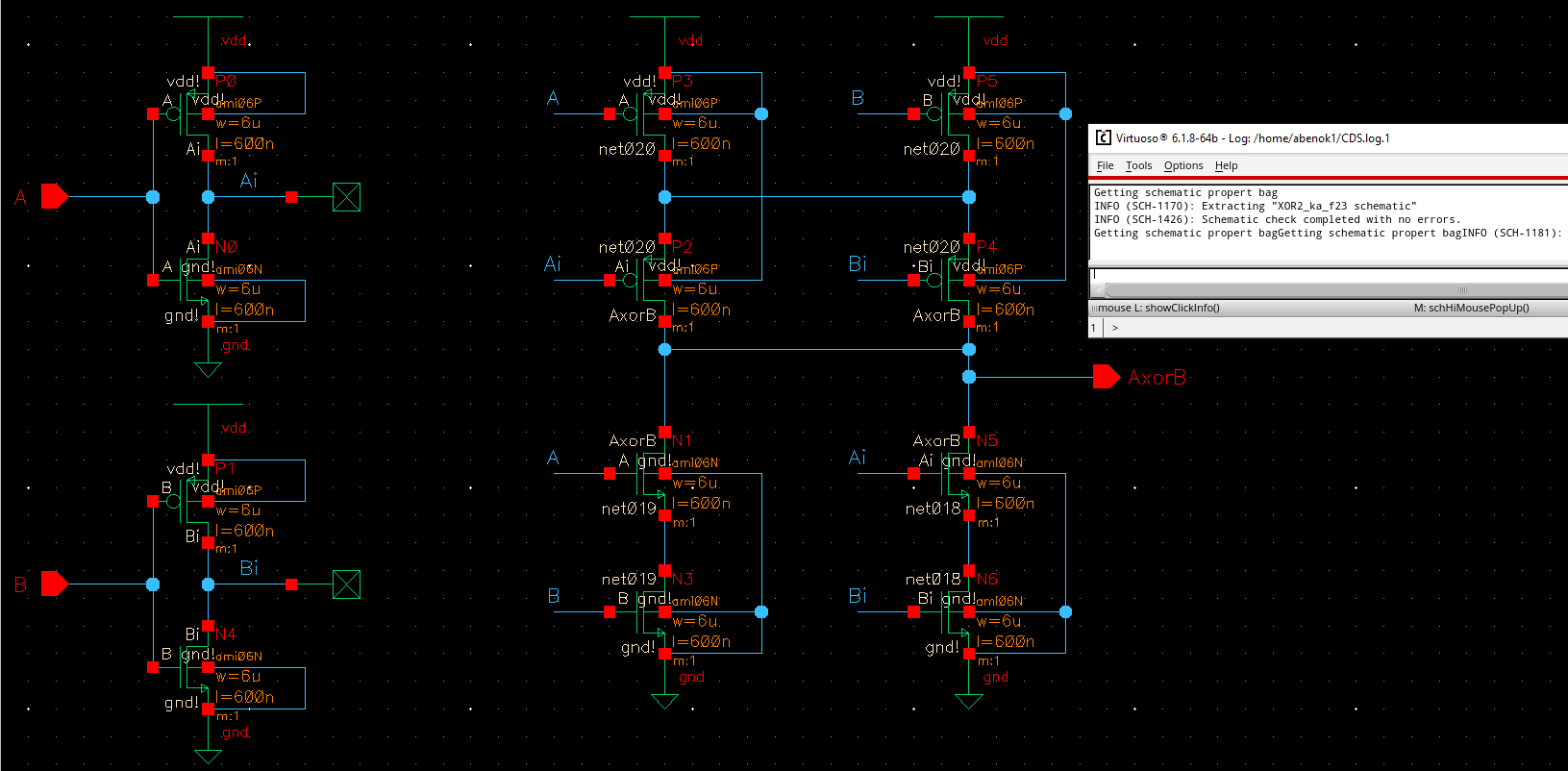
After this, we had to repeated the process for an XOR gate. 1) XOR schematic, 2) XOR symbol, 3) XOR layout, 4) XOR extracted view,
5) LVS results
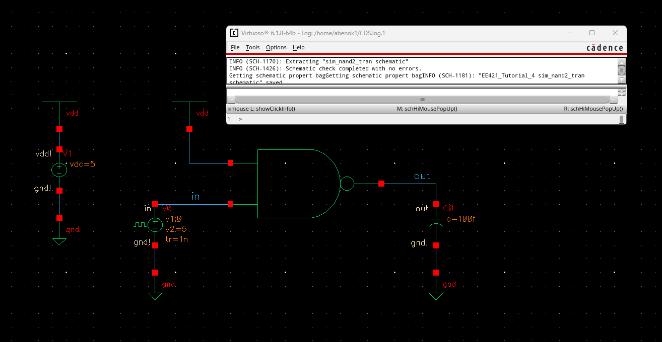
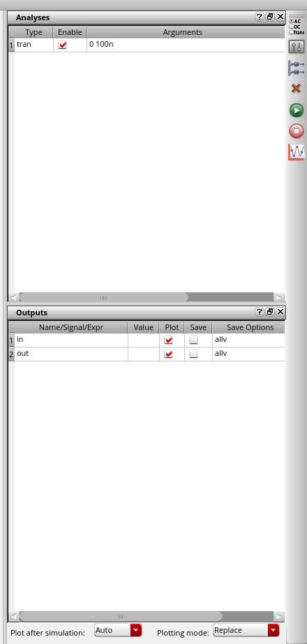
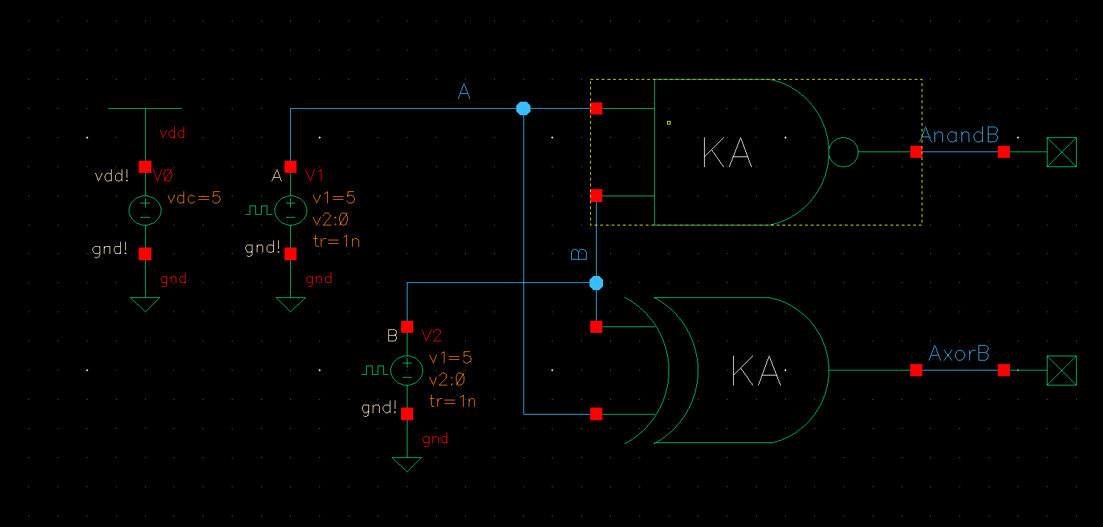
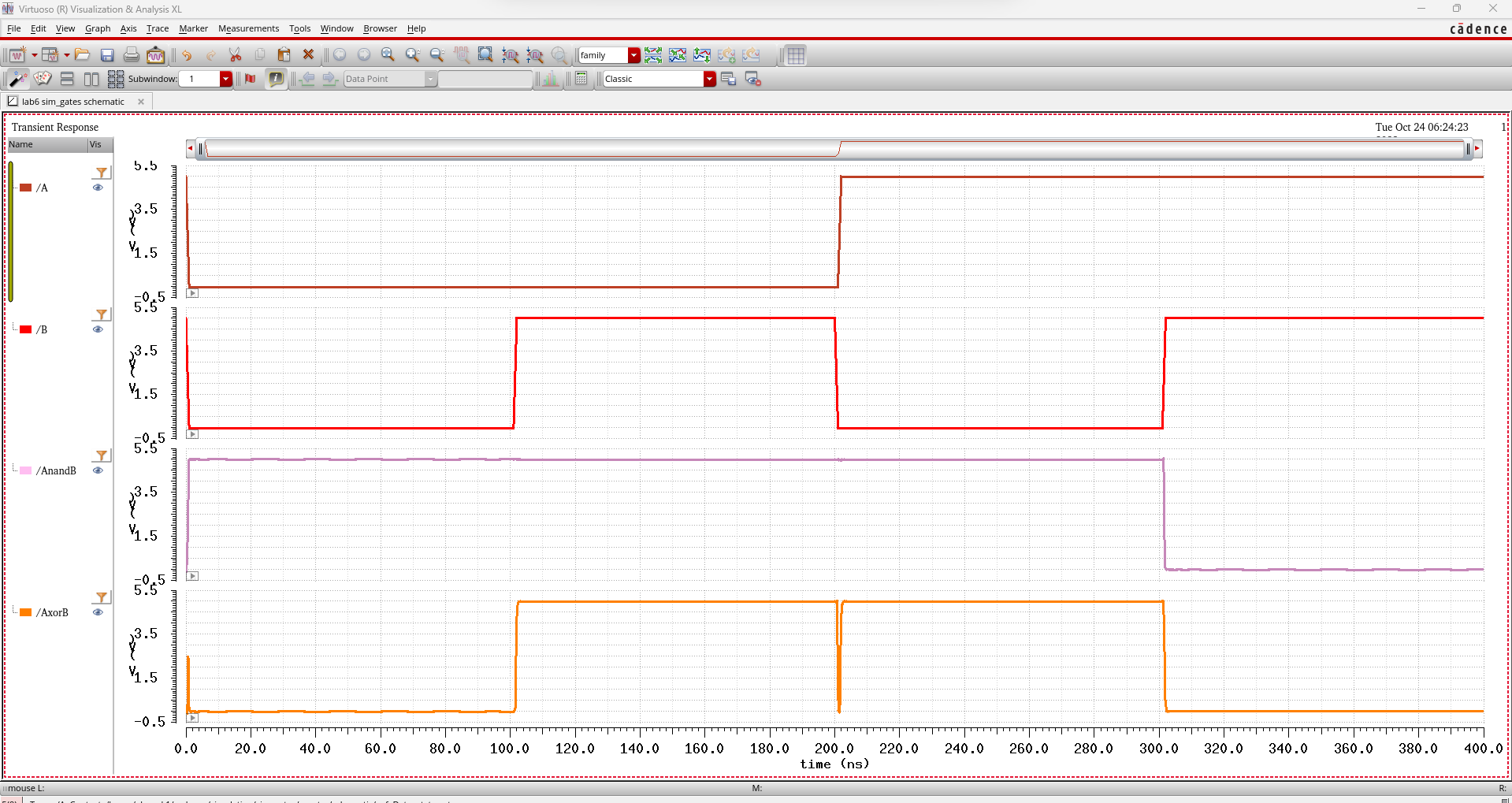
I then simulated my gates using the following circuit and got the following outputs.
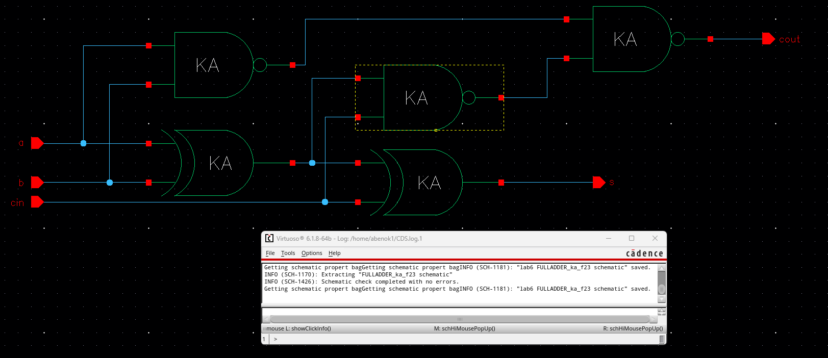
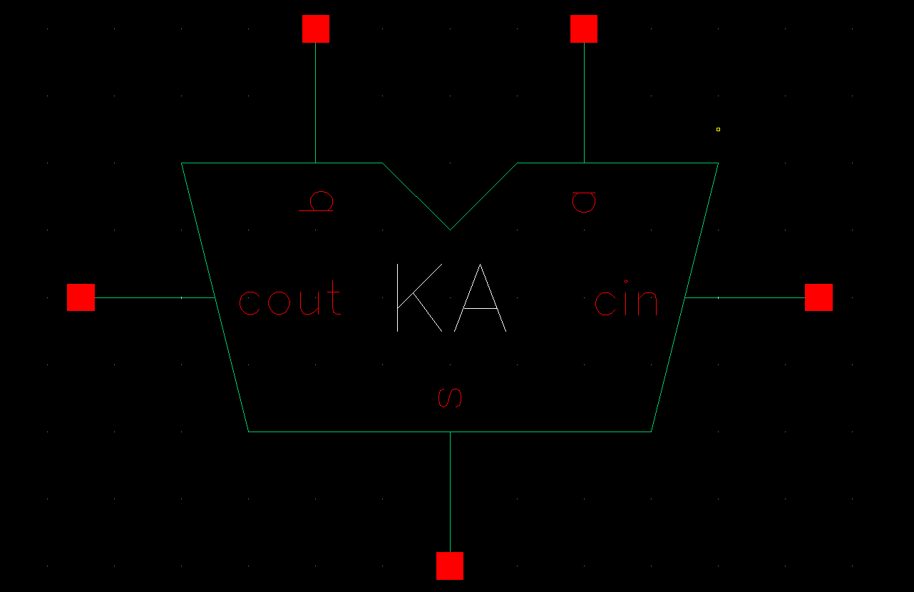
After confirming the operation of my gates, I used them to create a full adder. Below are the circuit and symbol I made for it.
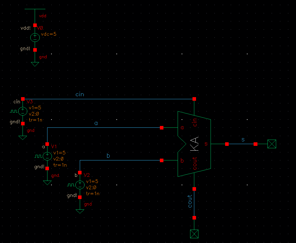
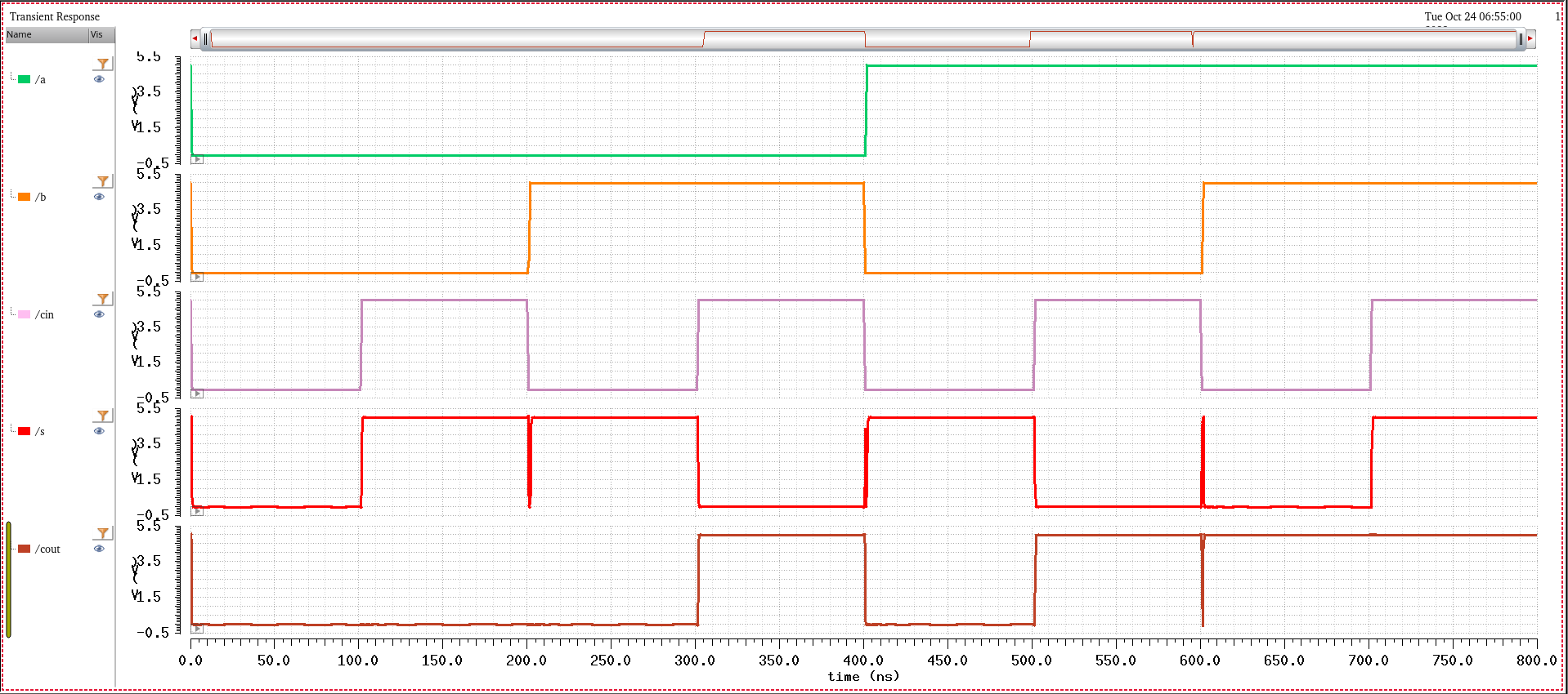
I then tested the operation of my full adder and got the following.
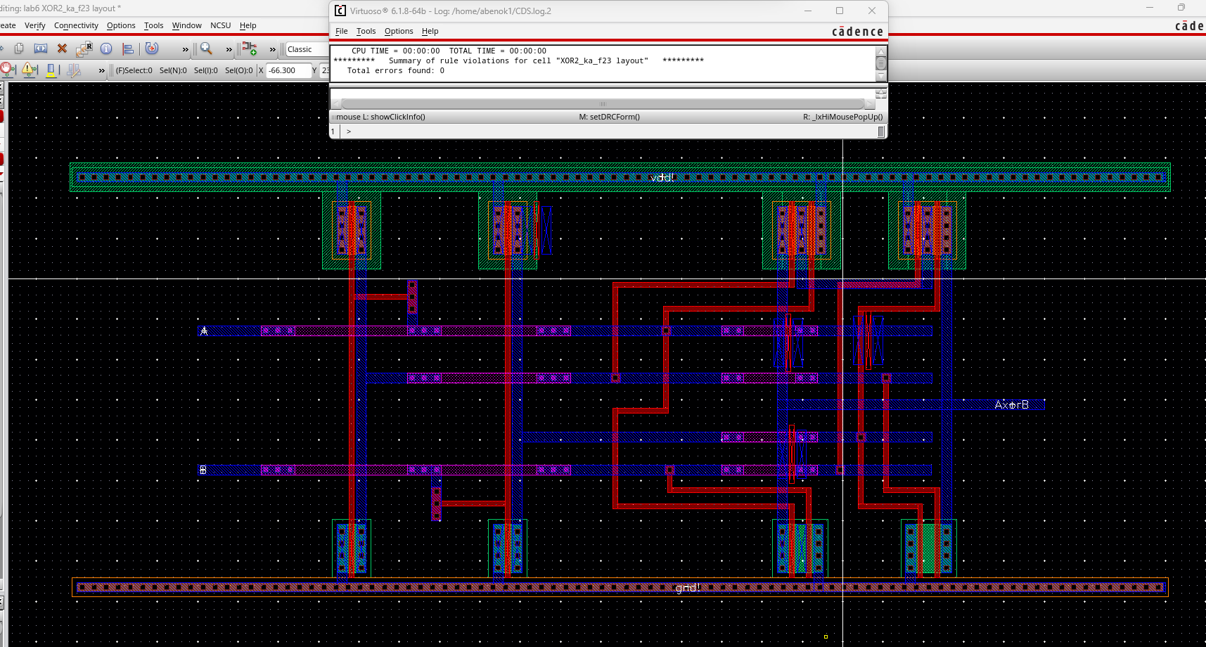
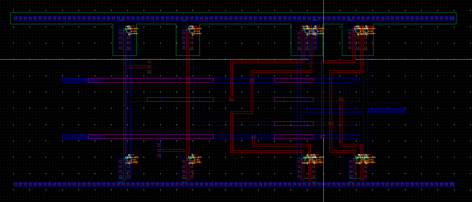
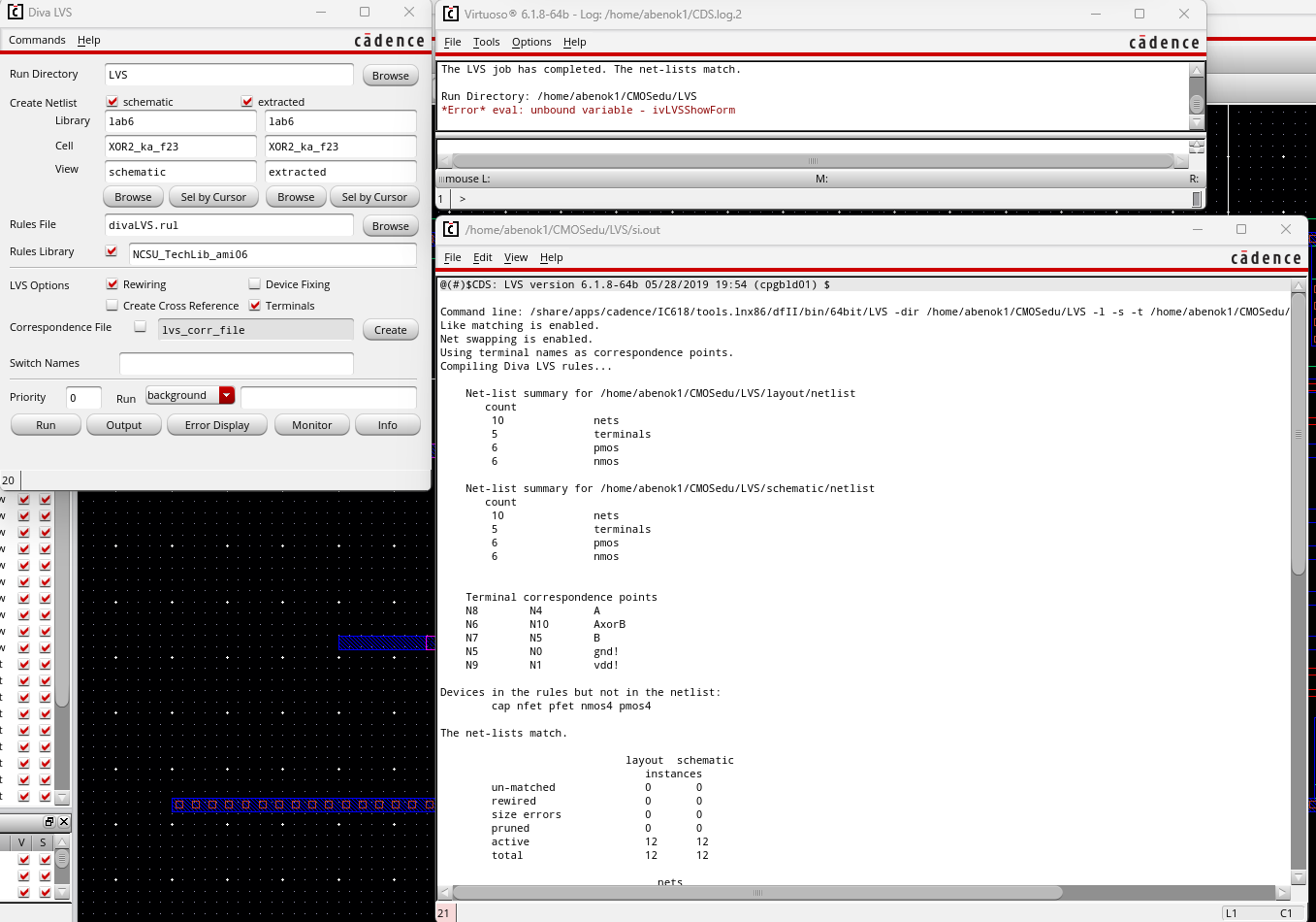
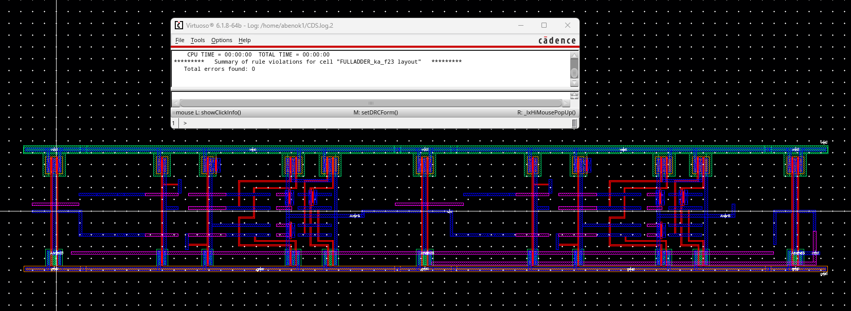
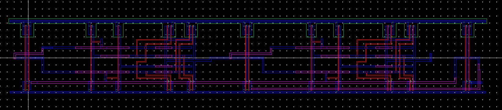
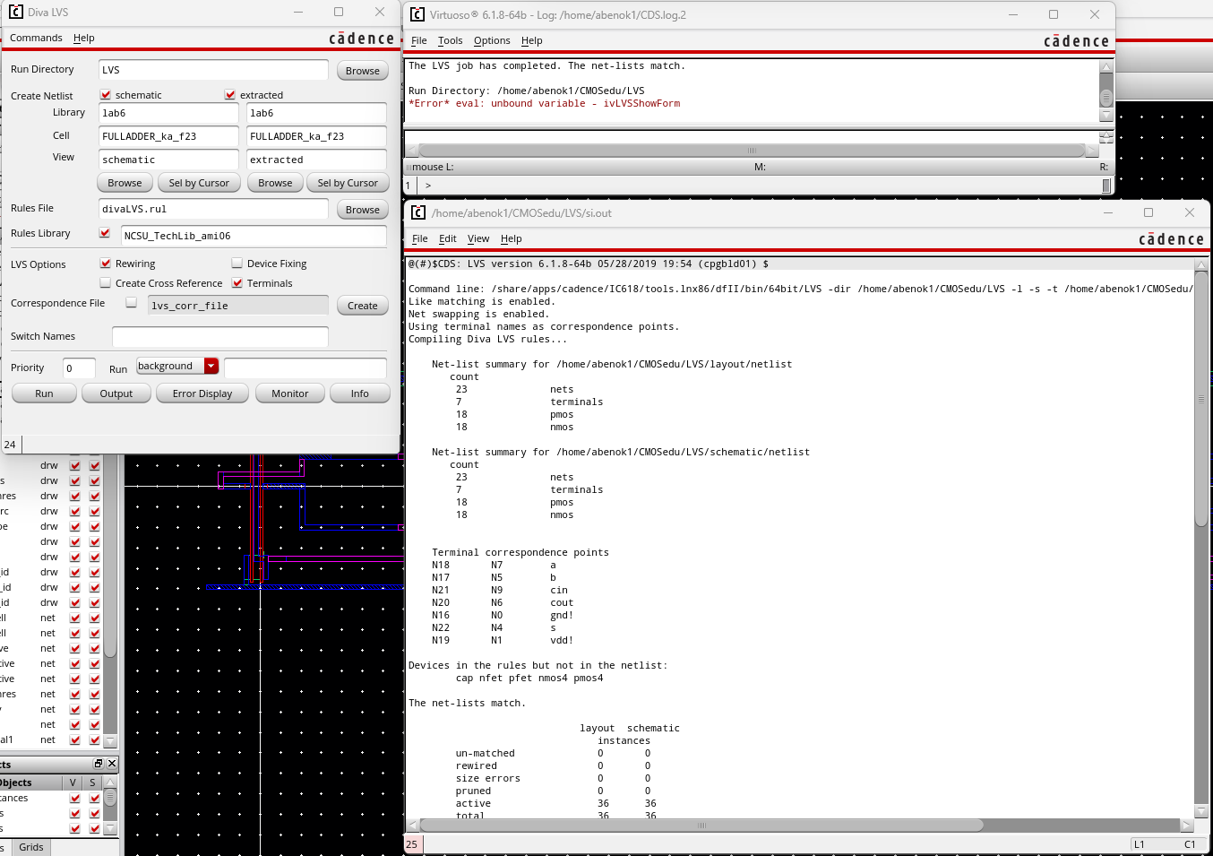
Lastly, I created the layouut for my fulladder ensuring a clean DRC and extracted it ensuring a clean LVS.1)
NAND schematic, 2) NAND symbol, 3) NAND layout, 4) NAND extracted view,
5) LVS results
Return to 421L Labs