Lab 4 - ECE 421L
Authored
by Kyle Abenojar, abenok1@unlv.nevada.edu
September 27th, 2023
Prelab:
For lab4, our prelab was to finish Tutorial 2.
To
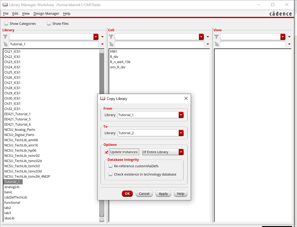
start tutorial 2, we copy our files from Tutorial 1 to Tutorial 2
making sure to update the instances so that Tutorial 2's files don't
stay dependent on Tutorial 1's.
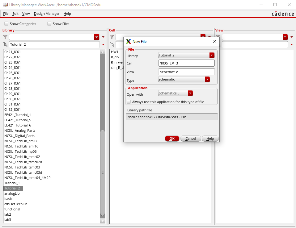
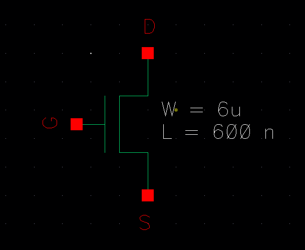
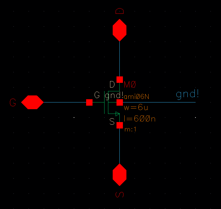
Next, we create a new schematic cell called NMOS_IV_3
In
the schematic view, we then add the NMOS symbol from the
NCSU_Analog_Parts library. We set the width and length as 6um and 600nm.
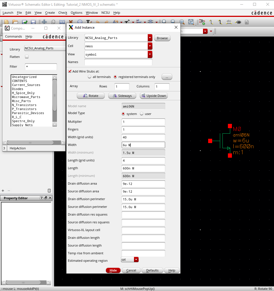
After adding the symbol, we add 3 pins: G, S and D with the I/O type set as inputoutput.
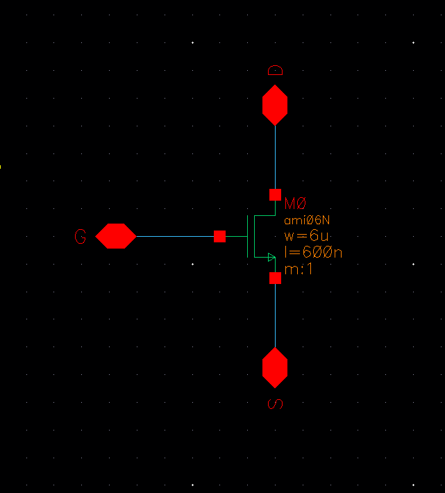
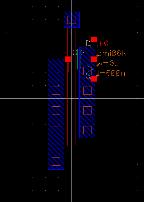
Next,
we create a symbol for our schematic by going into the create tab and
creating a symbol cellview from our current schematic cellview.
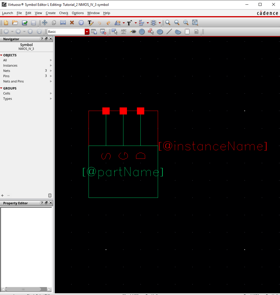
We then edit our symbol to look like the following below.
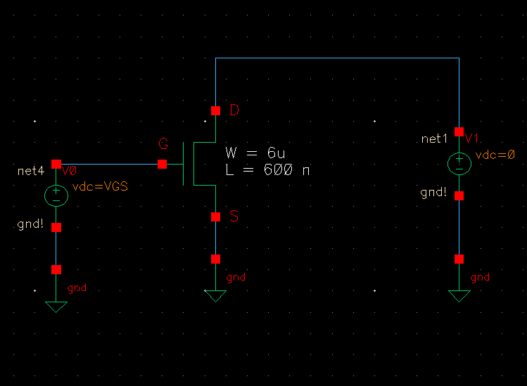
Next,
we create a new schematic in our Tutorial_2 library titled
sim_NMOS_IV_3 and create the following schematic using the symbol we
created in the steps above.
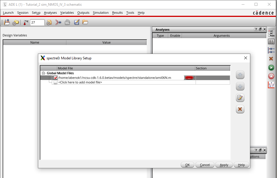
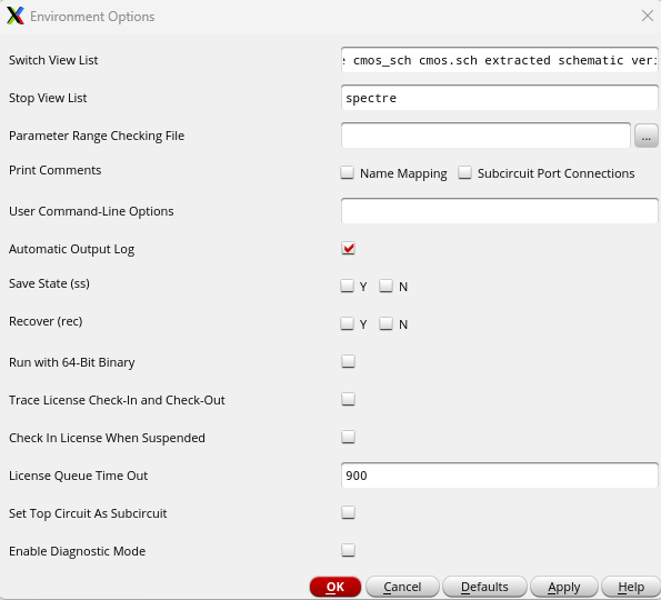
We then open the ADE L and edit the model library setup to the proper file.
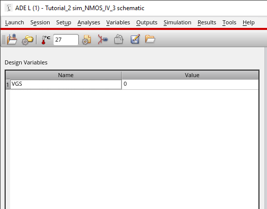
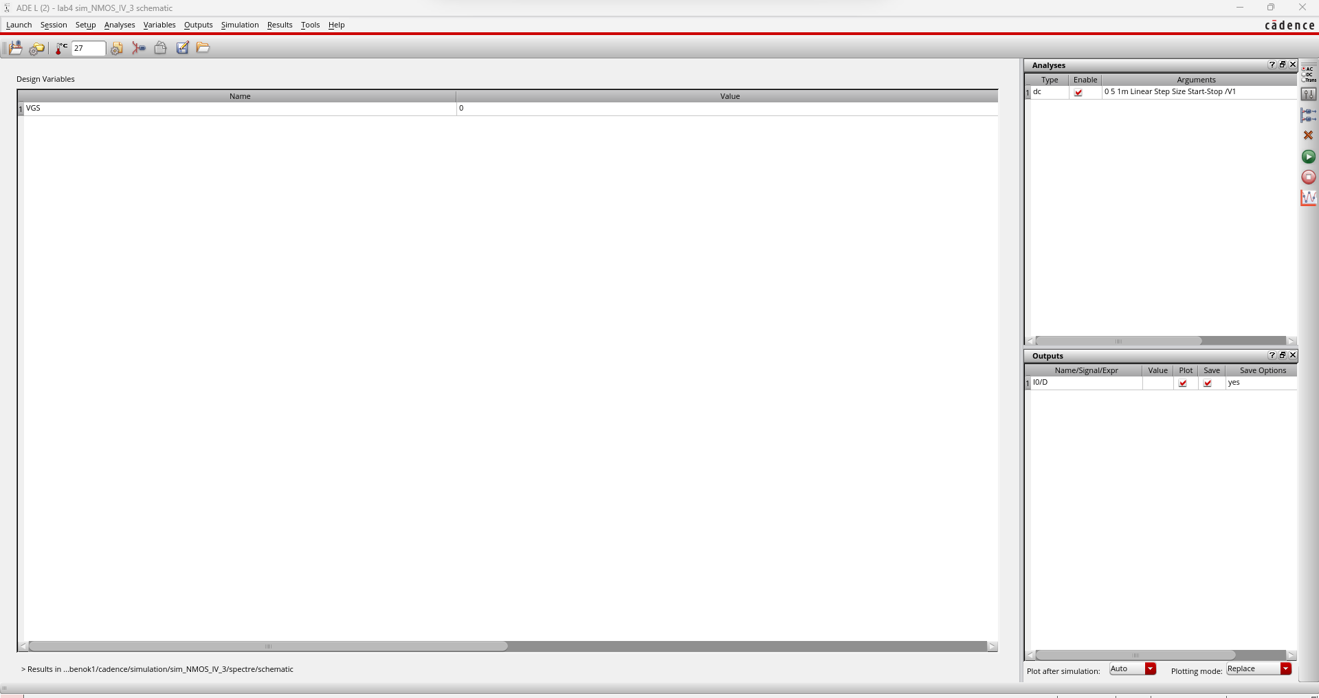
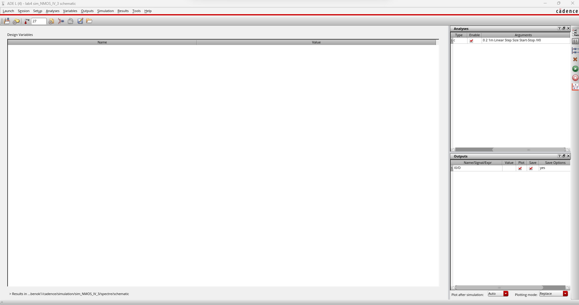
Next, we create a new variable called VGS and set the value to 0.
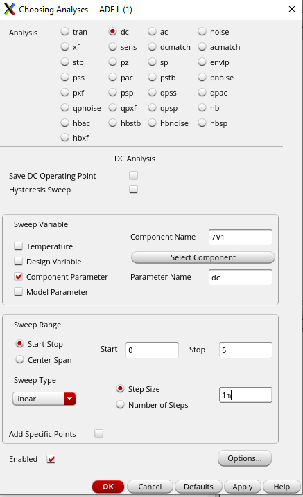
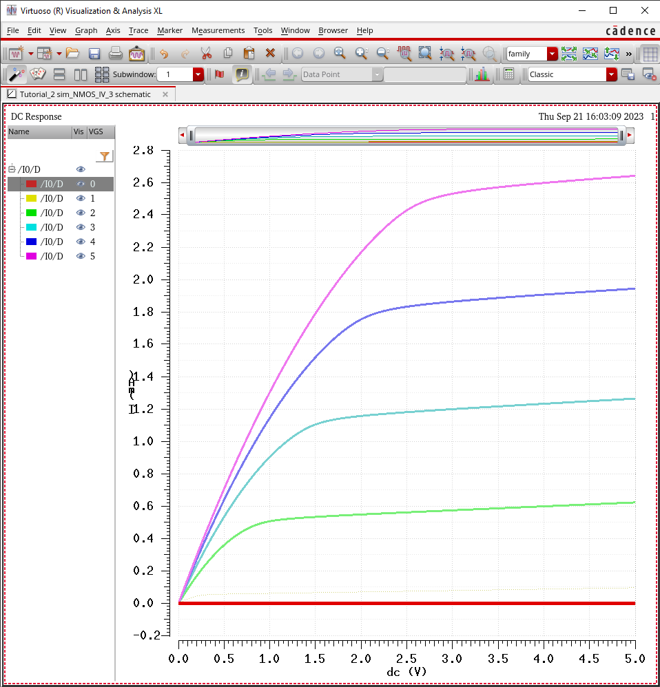
We then set a dc analysis with the following parameters below.
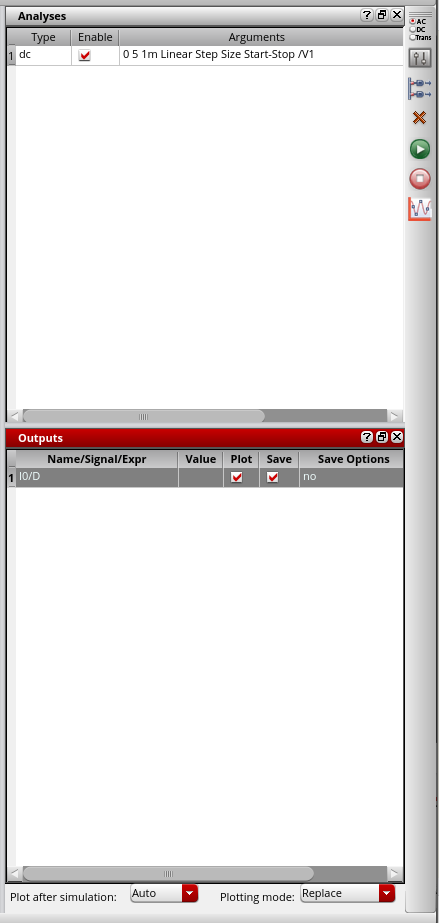
We
also choose the D pin to be plotted on the schematic ensuring that both
plotted and saved are selected. Our ADE L window now has this selected.
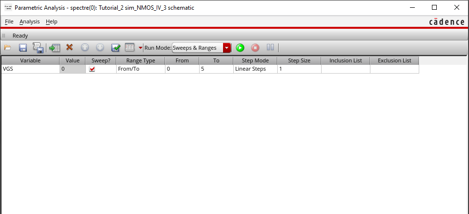
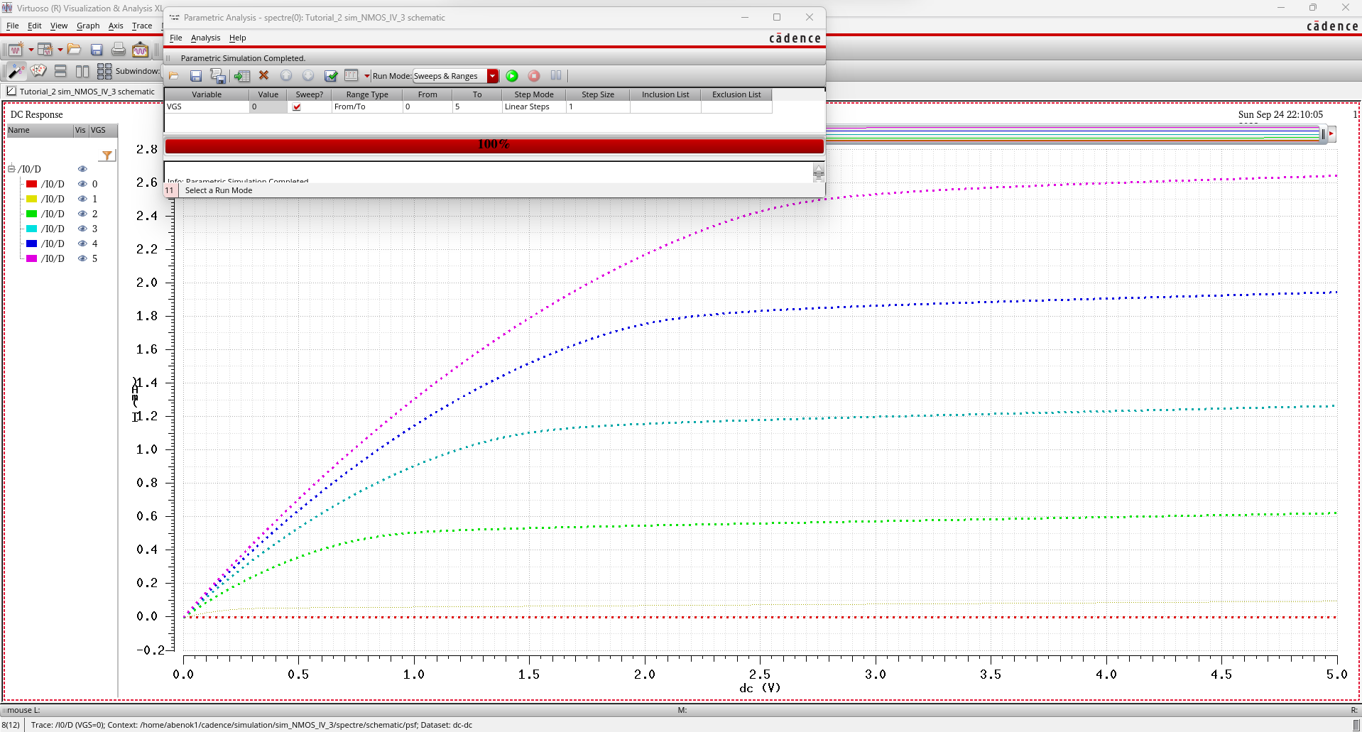
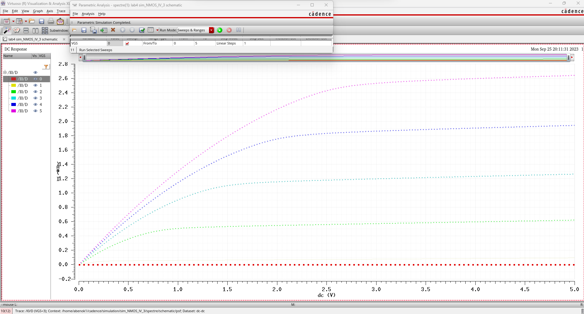
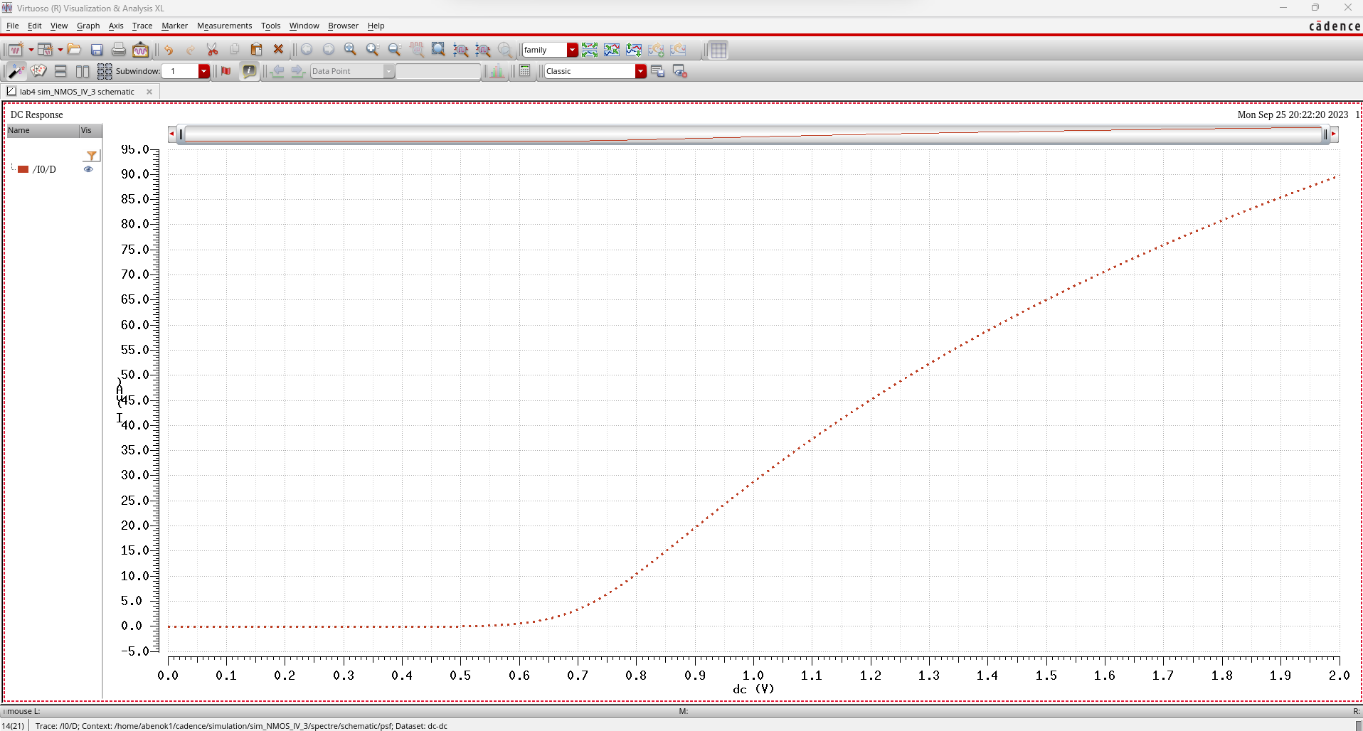
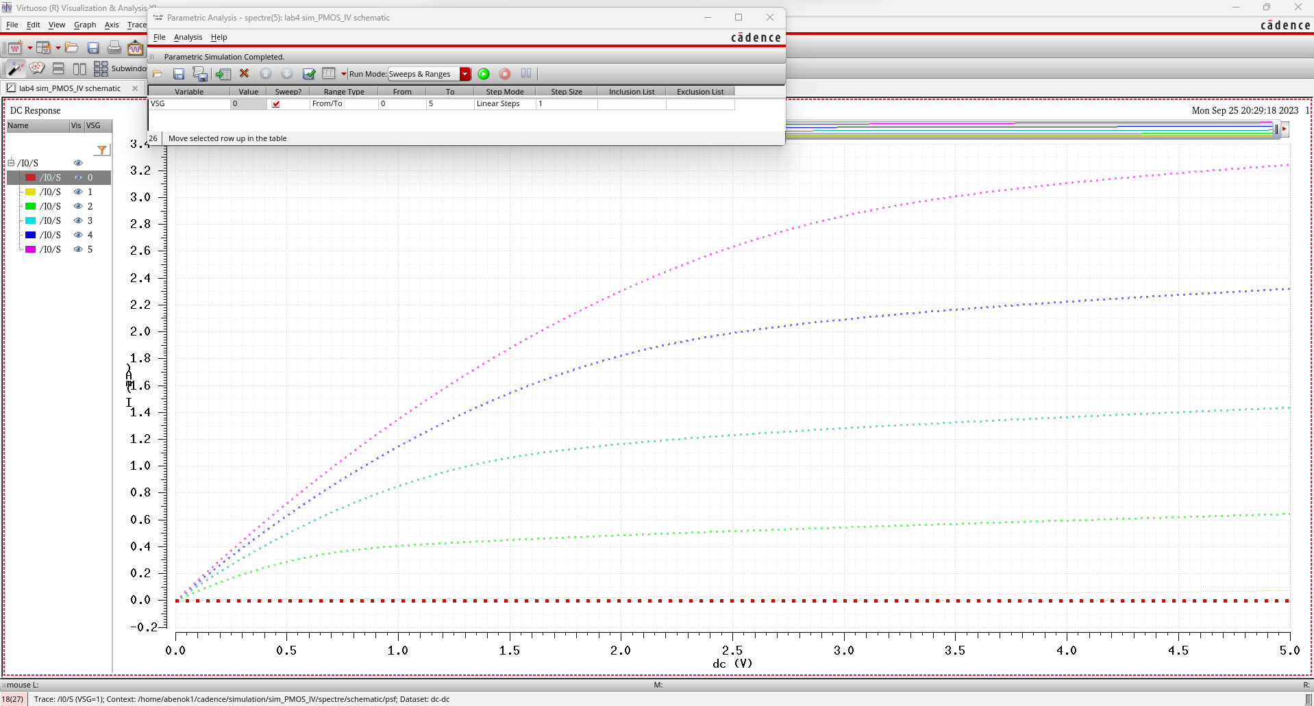
We then go into Tools and select Parametric Analysis and set the following parameters. We then simulate our schematic.
After plotting our output, we get the following graph.
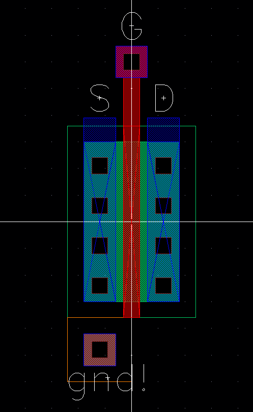
Next,
we create a layout view for our NMOS_IV_3 cell and add an instance of
an nmos cell making sure to set the proper length and width and a ptap
cell.
Next,
we add a m_poly cell as well and connect a poly rectangle from NMOS
cell to it. Then we add metal1 rectangles to connect to the source, the
drain, and gate. Lastly, we also add the S, G and D pins in the metal1
layer with the I/O type set to inputoutput.
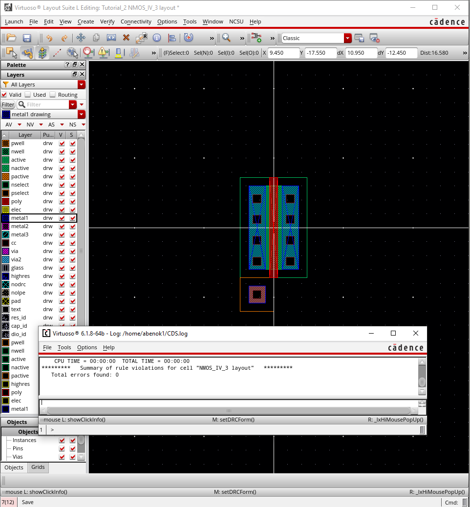
We
then extracted our layout view to get the following. However, we have
to make changes since our extracted view has 4 terminals whereas our
schematic only has 3.
So we go back into our layout view and change our S Pin and tie our ptap to gnd!.
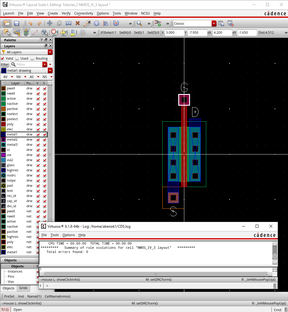
We
then get the following view when we extract our new layout. However, we
need to make one more change, so we go into our schematic view.
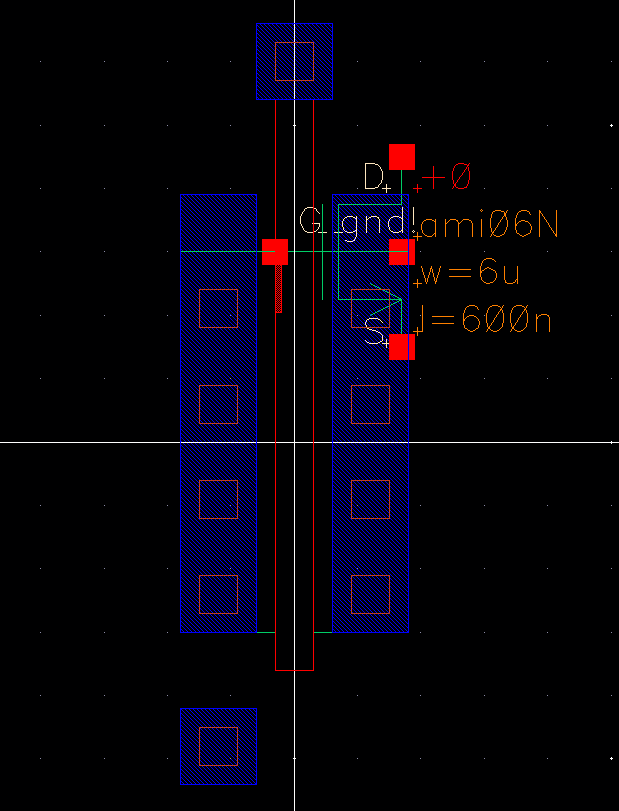
We change our nmos cell in our schematic to nmos4 so that we can discretely tie the p-substrate to gnd.
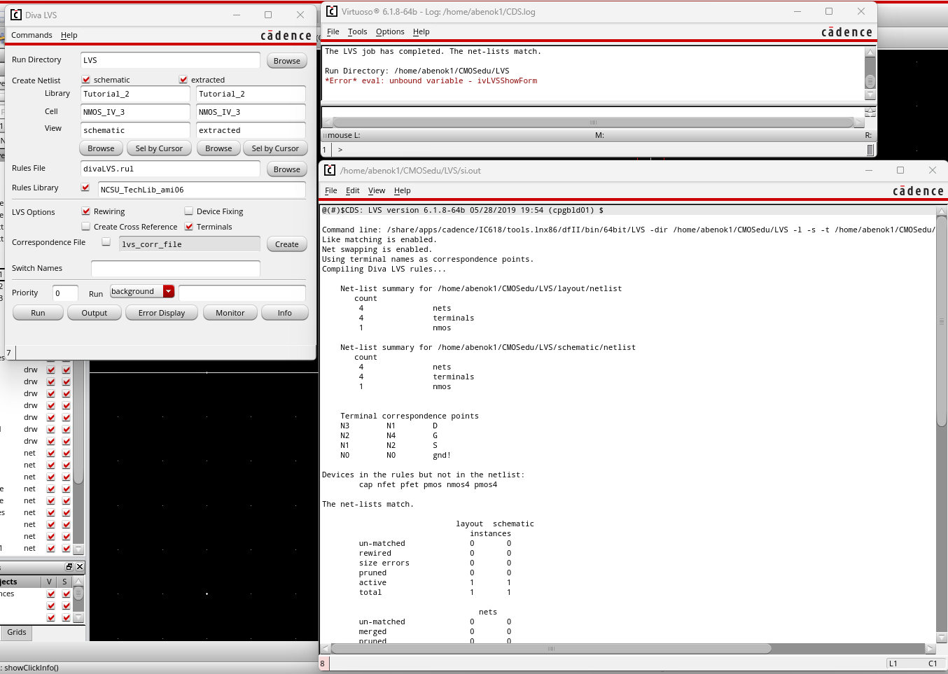
After
all of that, now we can go into our extracted view and perform an LVS.
We then see that it succeeded and that our netlists matched.
Now, we want to simulate
our extracted schematic. So we back to our sim_NMOS_IV_3 schematic and
open the ADE L. We then have to edit the environment view list by
adding 'extracted' before 'schematic'.
We then perform another parametric analysis to get the following curves.
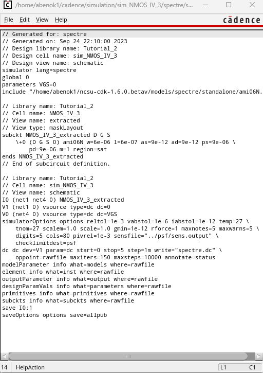
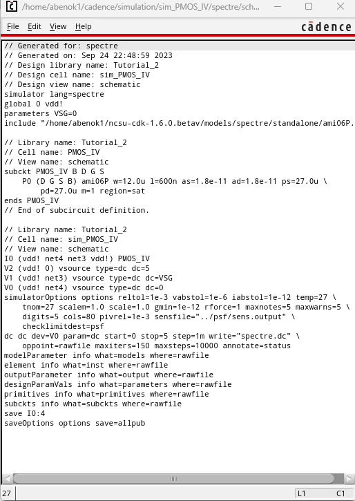
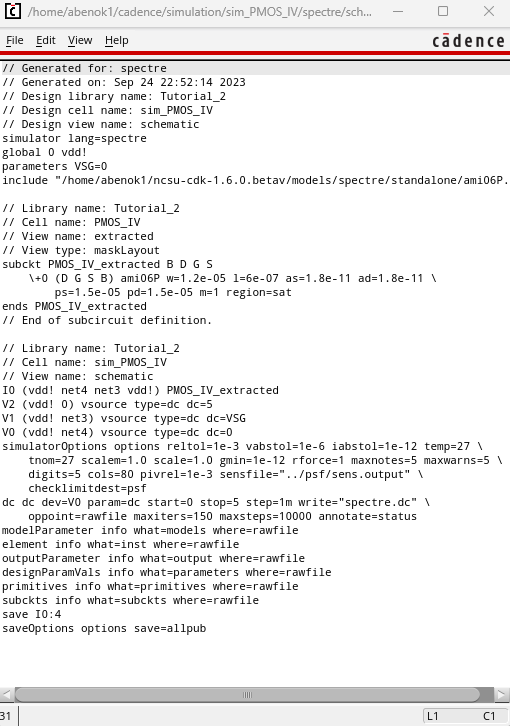
To ensure we are simulating the extracted view, we can go back to the ADE L and display the netlist.
Now
that we've gotten the hang of simulating an NMOS, we can simulate a
PMOS. We start by creating the following schematic using the pmos4 cell
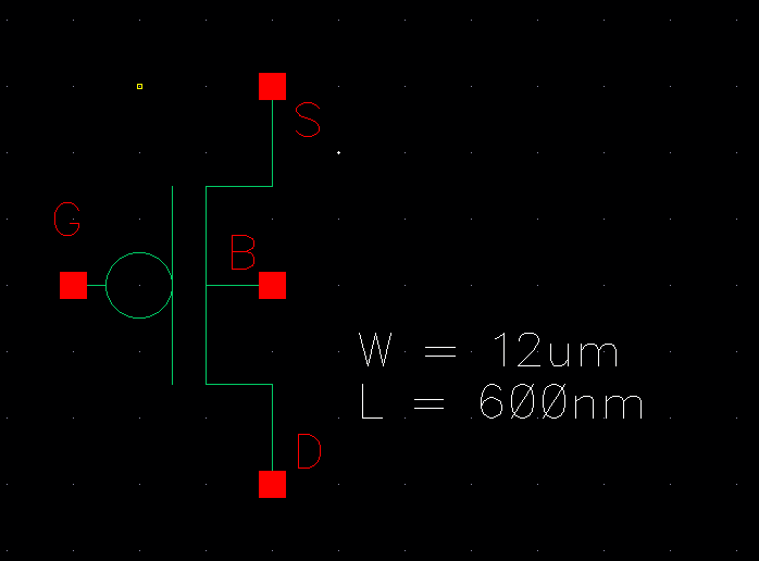
with a width of 12 um and a length of 600 nm.
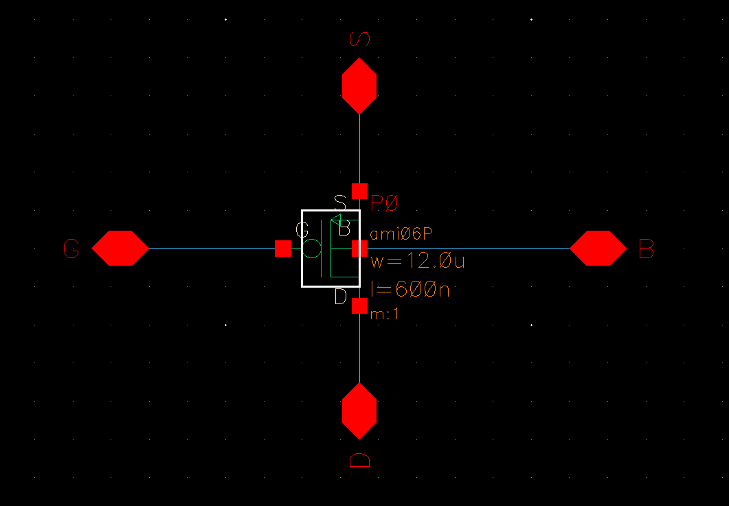
We then create the following symbol for our PMOS.
Then, we create a layout for our pmos using the pmos cell and an ntap.
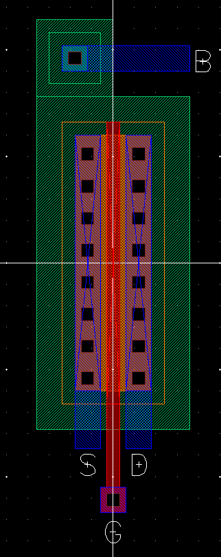
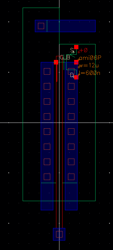
We can then extract our layout to get the following for our extracted view.
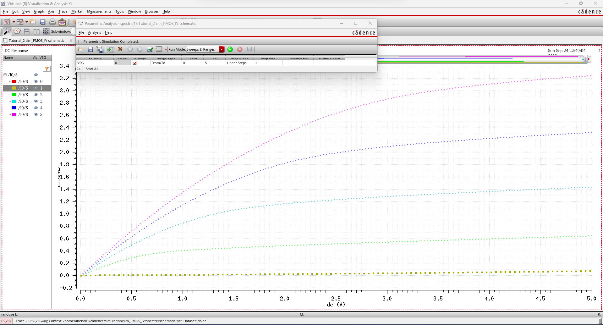
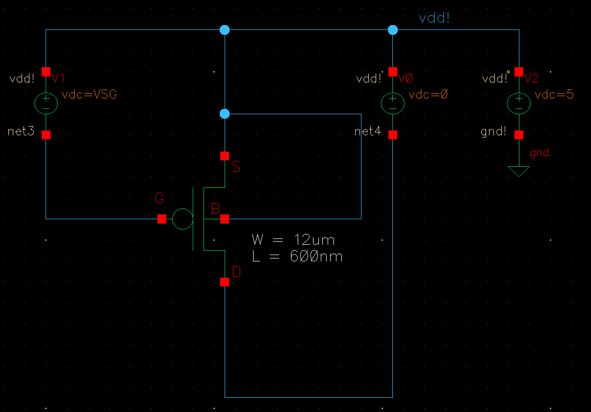
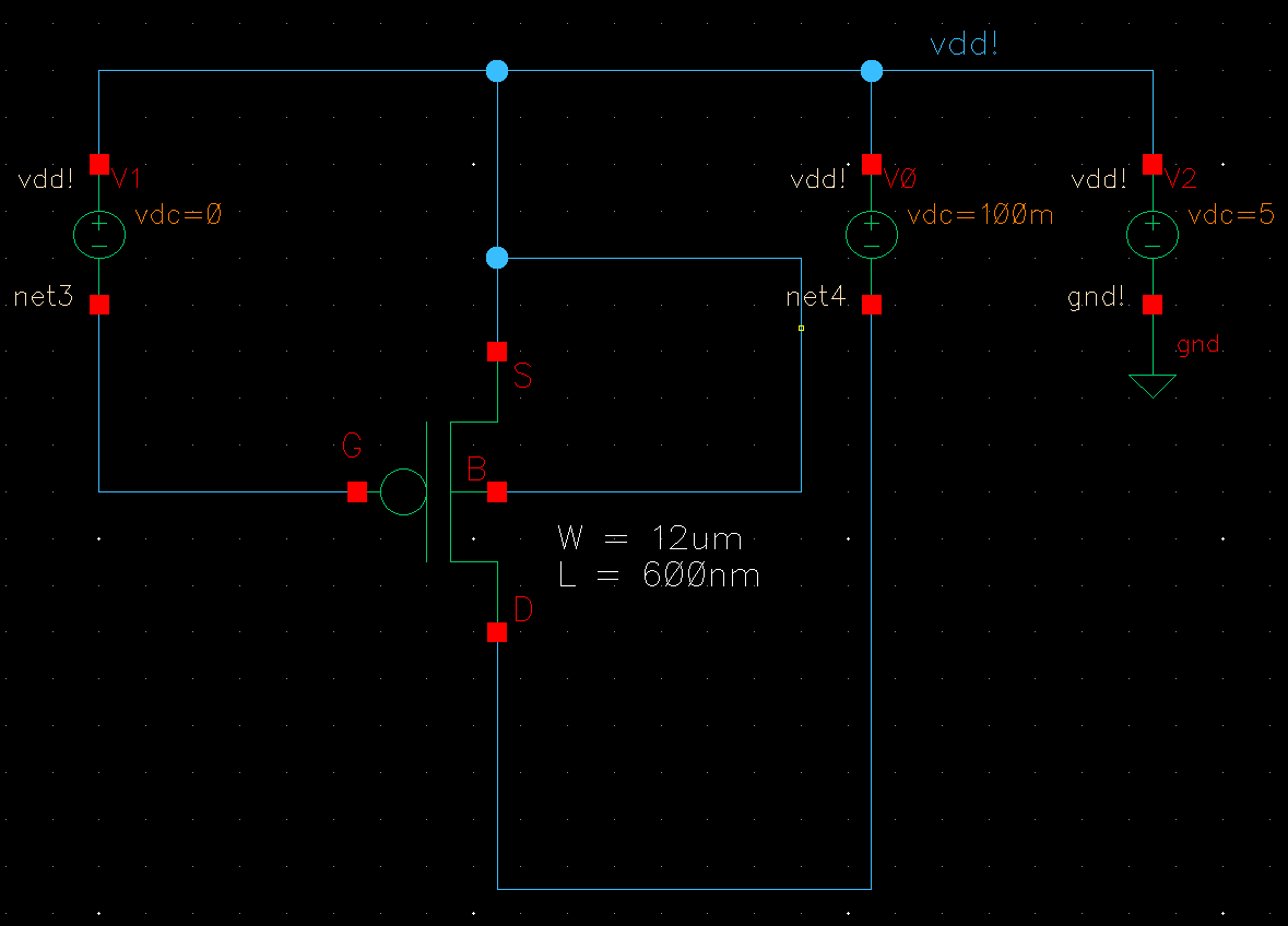
Now, we go to simulate our PMOS. We create a new schematic titled sim_PMOS_IV and draft the following schematic.
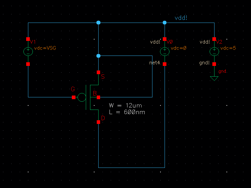
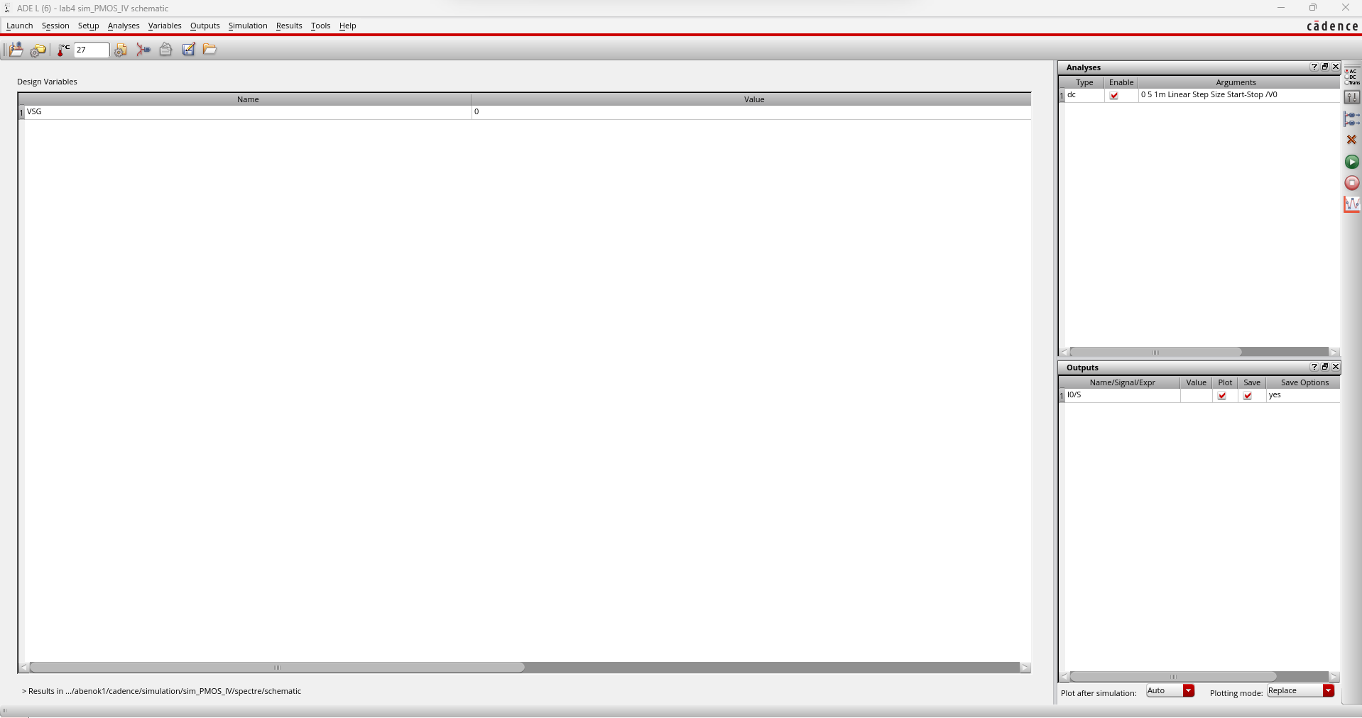
Simulating
the PMOS is very similar to simulating the NMOS with the main
differences being that we have to set the model library toami06P.m and
that we set our voltage source as VSG. After simulating, we get the
following curves.
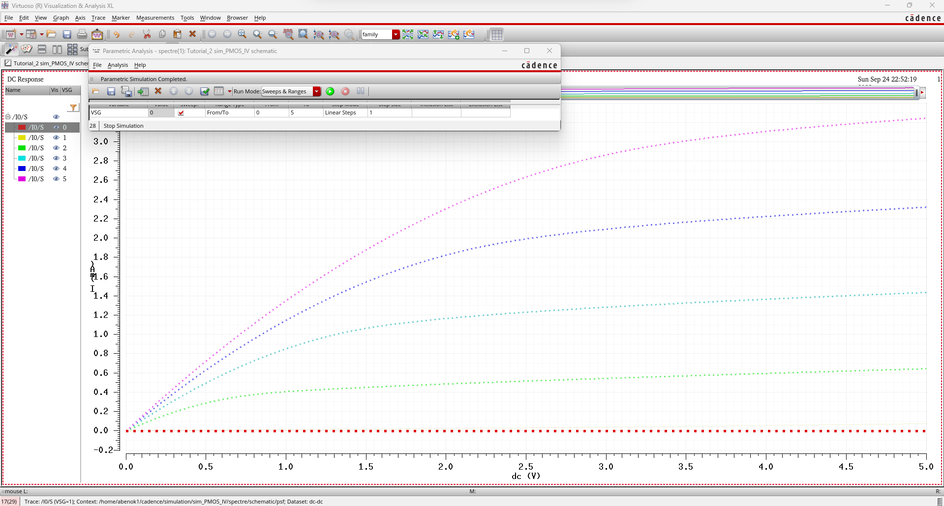
Here,
we see that we simulated the schematic first. Now we go onto simulate
the extracted schematic the same way we did for the NMOS.
Lastly, we simulate the extracted schematic and we get the following graph.
Lab Report:
In this lab, we were tasked with creating 4 different schematics with 4 different simulations.
These
are my results for simulating ID vs VDS of an NMOS device for VGS
varying from 0V to 5V in 1V steps while VDS varies from 0 to 5V
in 1mV steps. 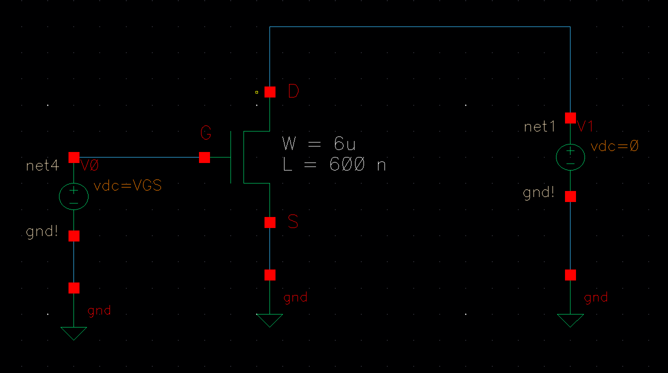
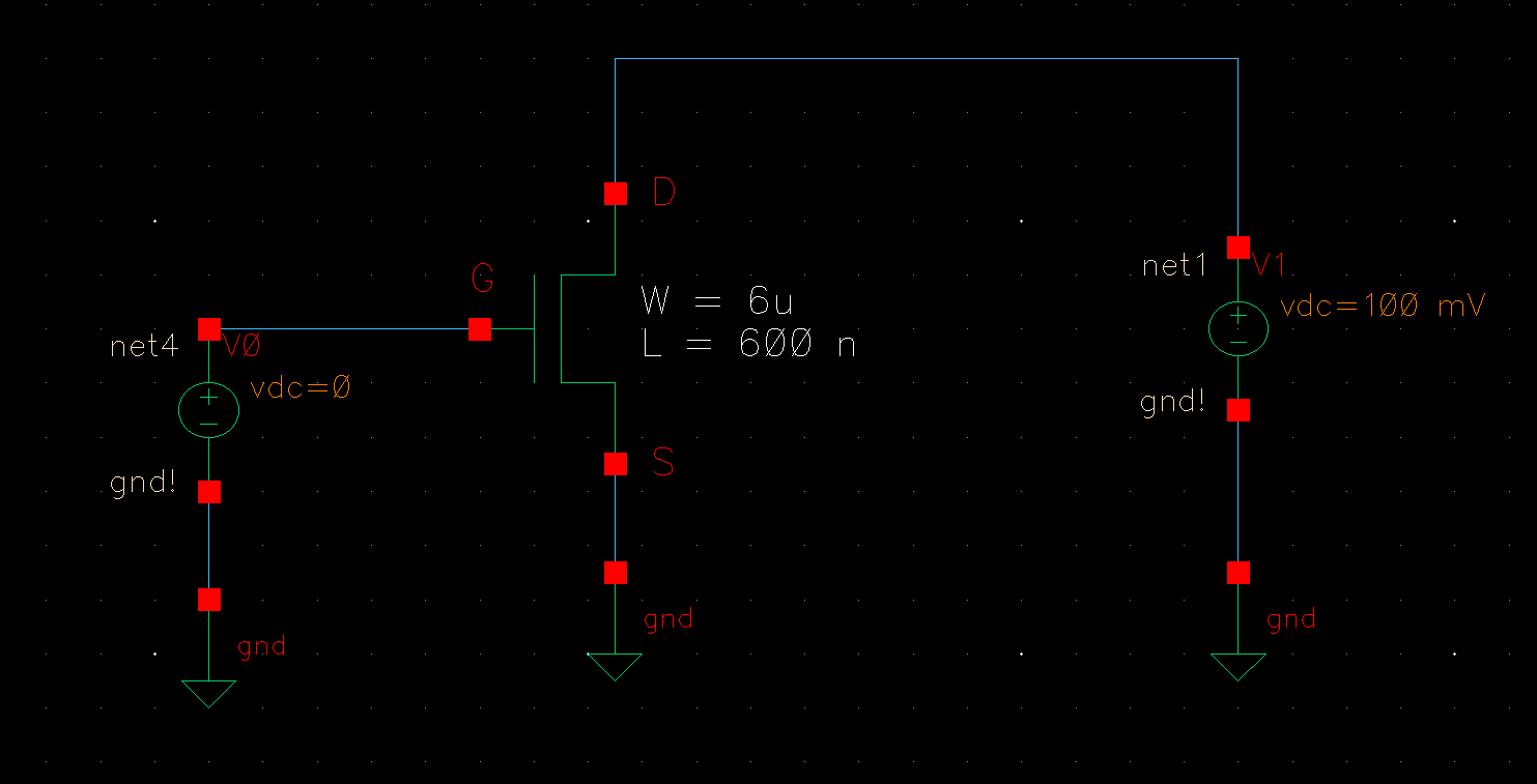
These are my results for simulating ID vs VGS of an NMOS device for VDS = 100 mV while VGS varies from 0 to 2V in 1mV
steps.
These are my results for simulating ID vs VSD of a PMOS device for
VSG varying from 0V to 5V in 1V steps while VSD varies from 0 to 5V in
1mV steps.
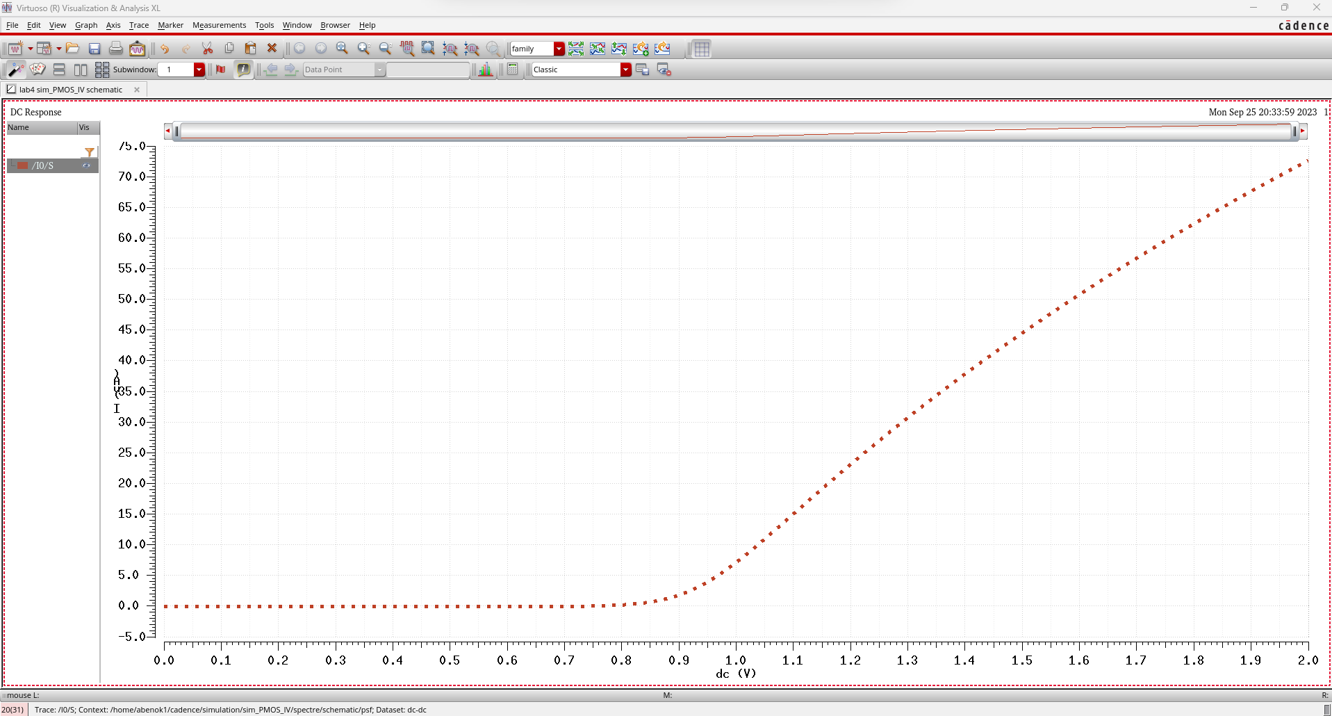
These are my results for simulating ID vs VSG of a PMOS device for VSD = 100 mV while VSG varies from 0 to 2V in 1mV
steps.
Next, we had to create a new schematic of our NMOS with the MOSFET terminals connected to probe pads.
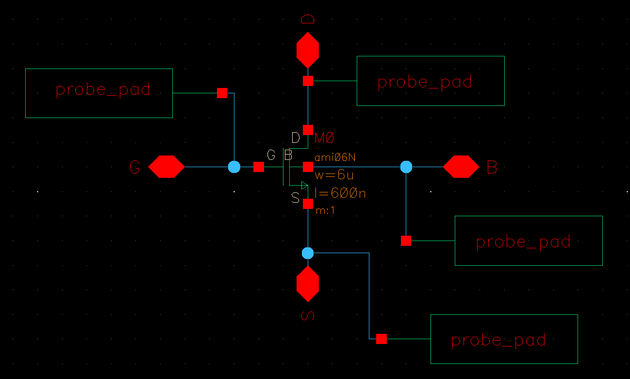
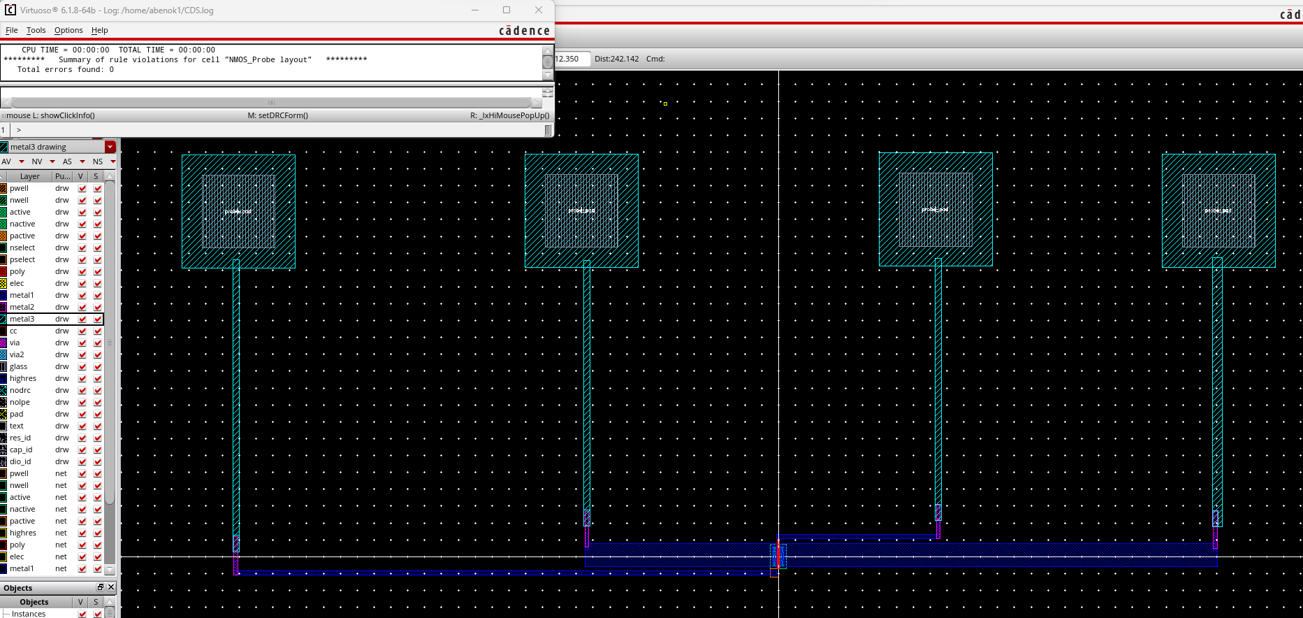
I then created a new layout for my NMOS connected to probe pads. I also DRC'ed my layout to ensure there are no errors.
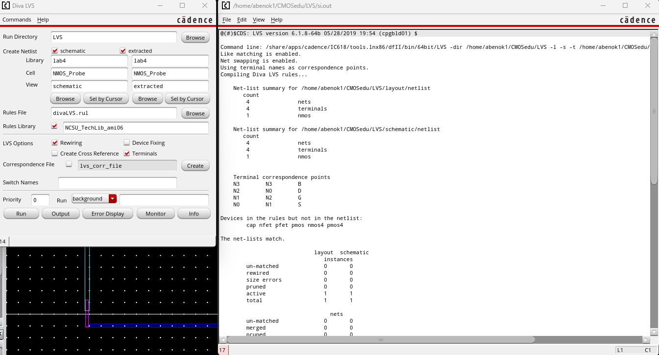
I then extracted my new layout and performed an LVS to check if the netlists matched.
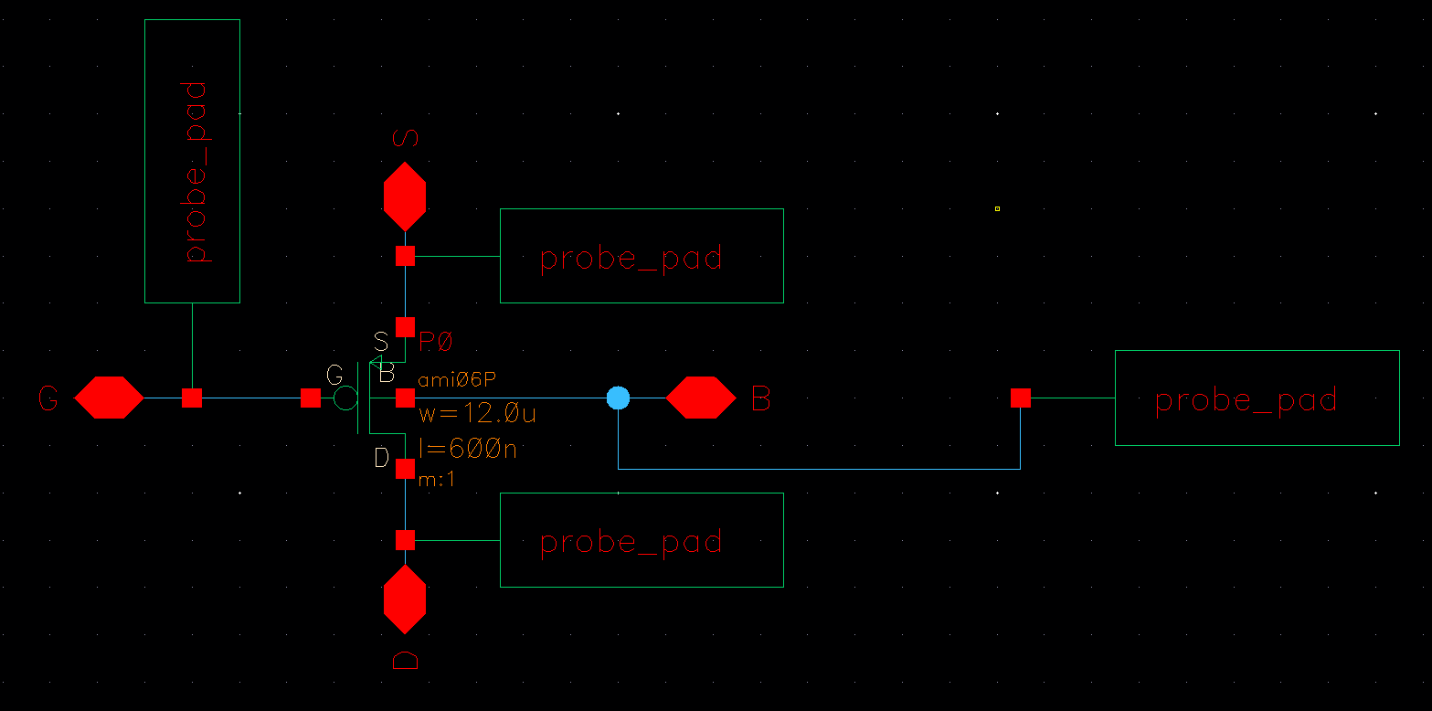
Next, we had to create a new schematic of our PMOS with the MOSFET terminals connected to probe pads.
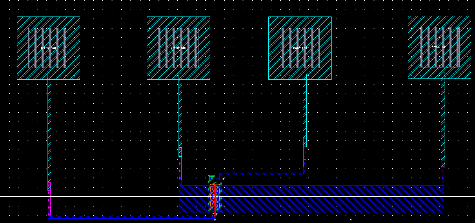
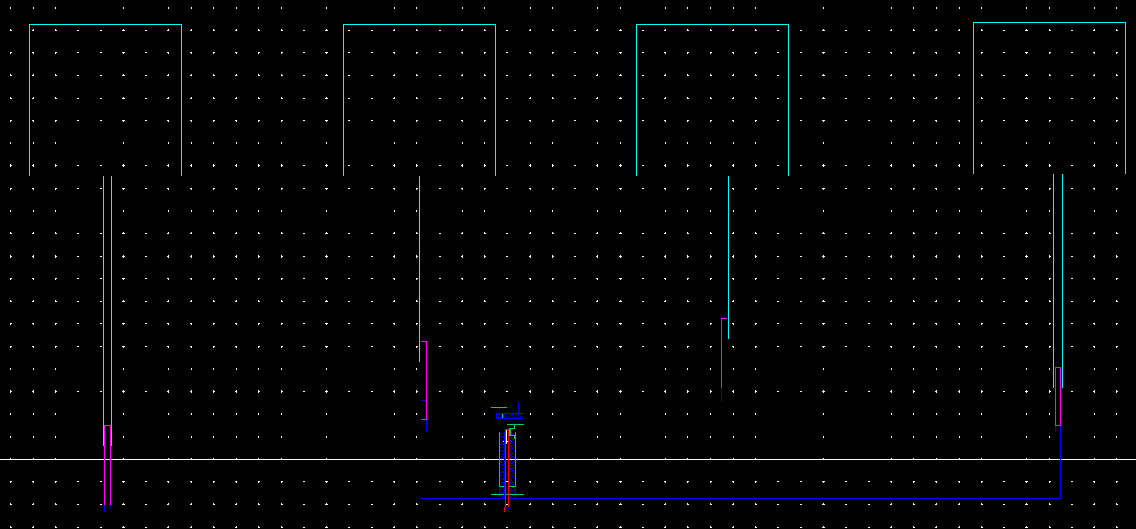
I then created a new layout for my PMOS connected to probe pads. I also DRC'ed my layout to ensure there are no errors
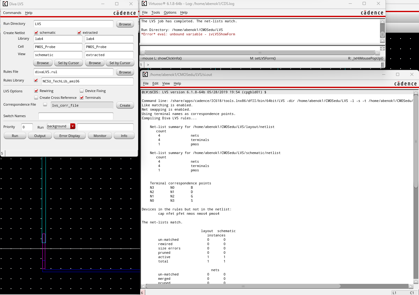
Lastly, I then extracted my new layout and performed an LVS to check if the netlists matched.
Return to 421L Labs