Lab 3 - ECE 421L
Authored
by Kyle Abenojar, abenok1@unlv.nevada.edu
September 20th, 2023
Prelab:
In this lab, we were tasked with continuing Tutorial 1 for the prelab.
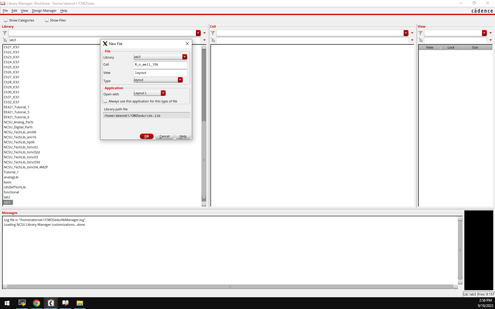
I started off by creating a new layout cell view titled R_n_well_10k. This will hold my n_well resistor layout view.
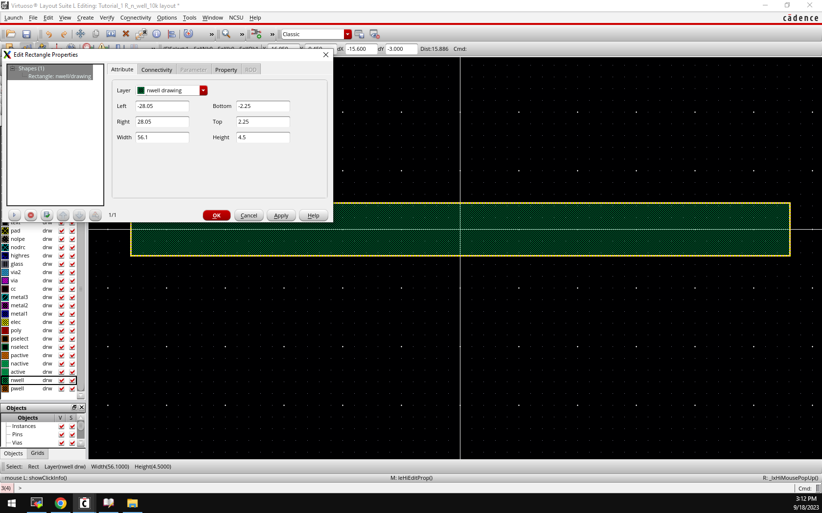
Next, in the layout suite, I used the R key to create a rectangle
while also making sure that I have the n_well layer selected. I then
clicked the rectangle and used the Q key to change the properties
to make it a 56.1 by 5 rectangle. These dimensions were used to create
a rectangle with a resistance of 10K with dimensions divisible by .15
since the program needs the shape to be on the grid or else errors will
occur.
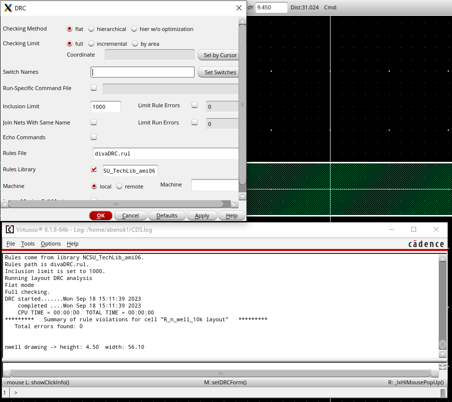
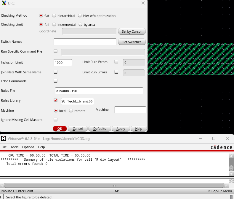
After creating my rectangle, I clicked the Verify Tab to DRC my layout, and as shown below, 0 errors were detected.
I
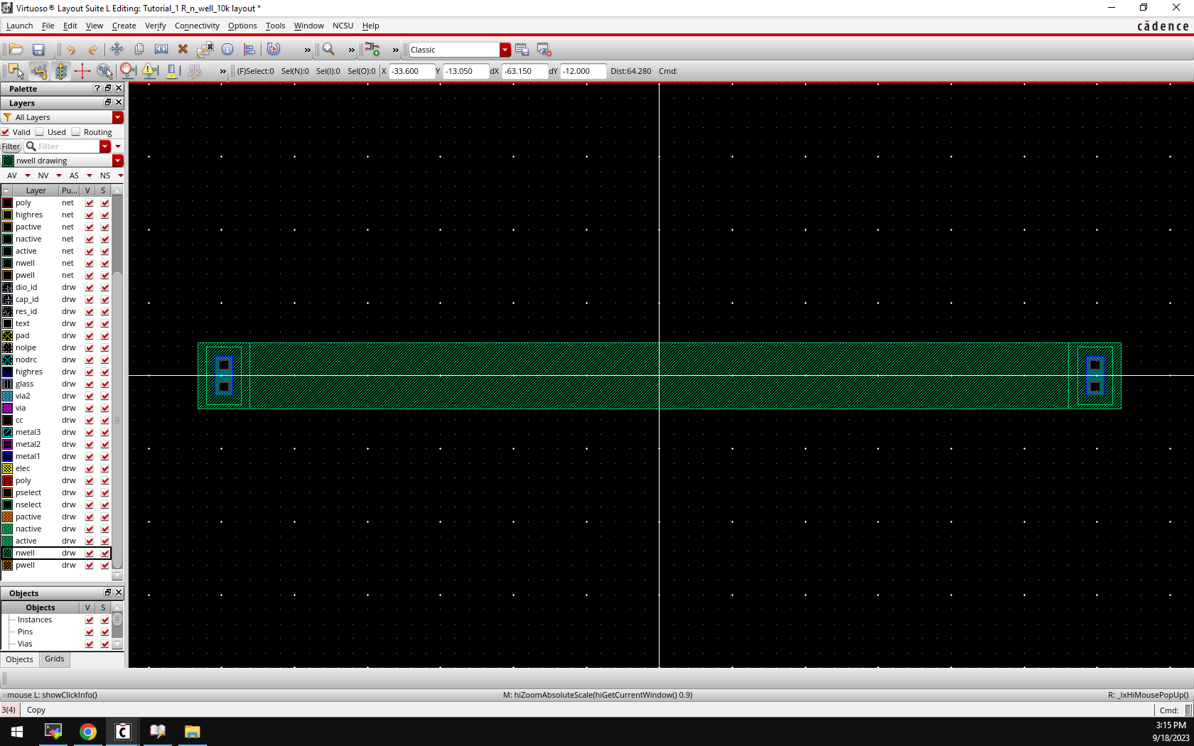
then clicked the I key to create a new instance. After navigating to
the NCSU Analog Library, I was able to add two ntaps to my layout. The
two ntaps have 2 connections per row. I then placed the ntaps on the
right and left side of my n_well.
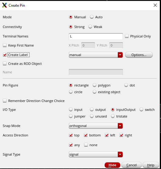
Next,
I needed to make pins for my resistor. By going in the Create tab, I
can open the Create Pin window. Here, I make sure that a new label in
created when I generate the pin. I create a pin for both the left (L)
and right (R) ntaps.
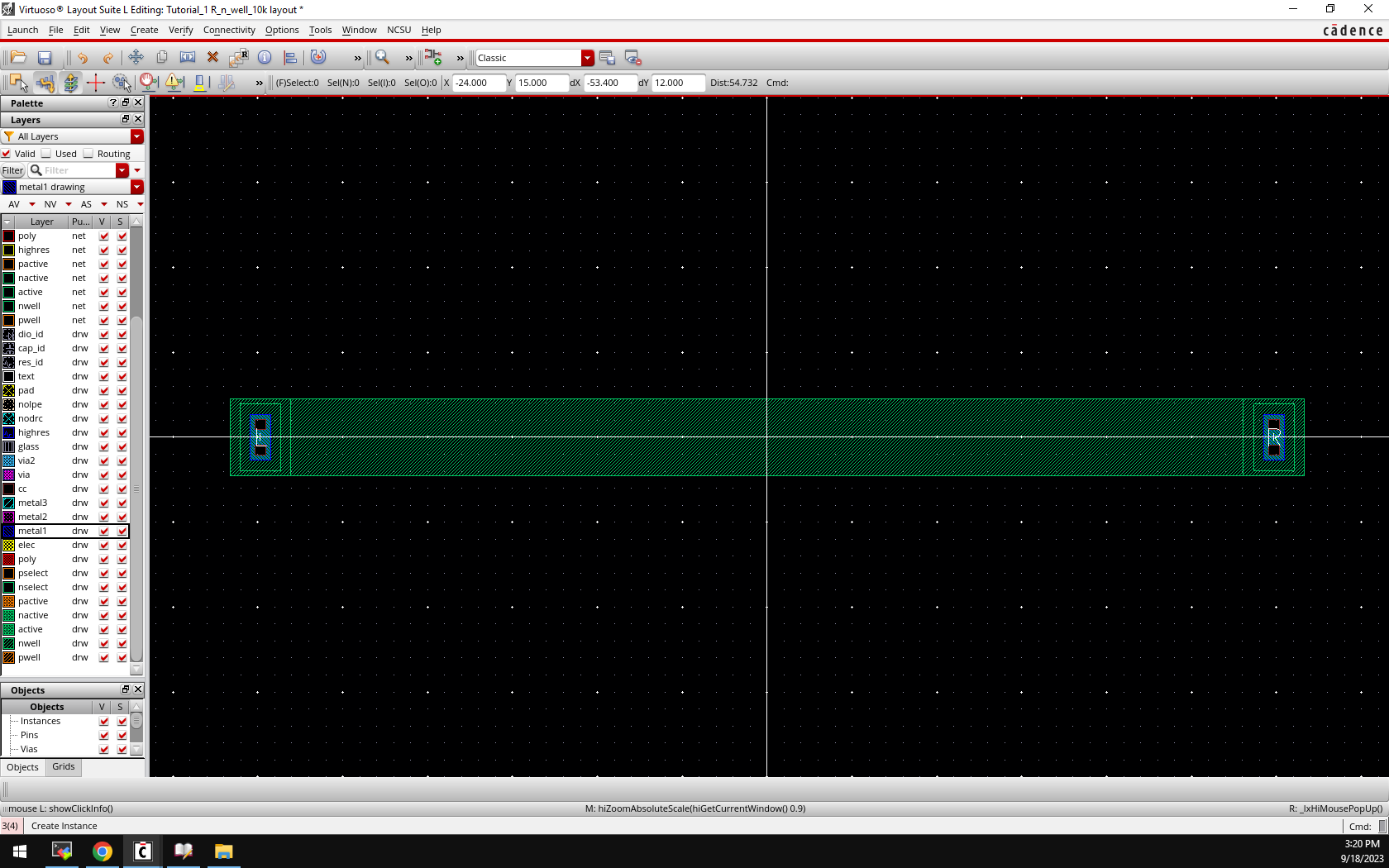
After generating my pins and placing them on the metal contacts of my ntaps, this is what I was left with.
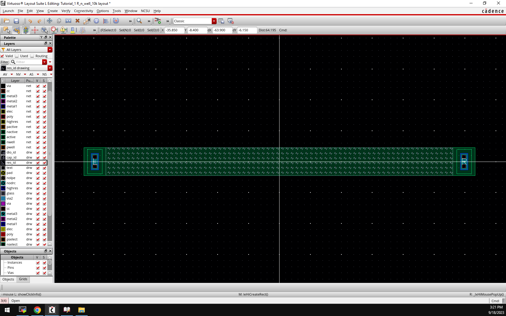
Next,
I chose the res_id layer and placed a rectangle over my n_well layer.
What this does is tells the program that the n_well is being used as a
resistor. Otherwise, DRC'ing the layout will spit out an error since it
will think that the L and R pins are defining the same thing.
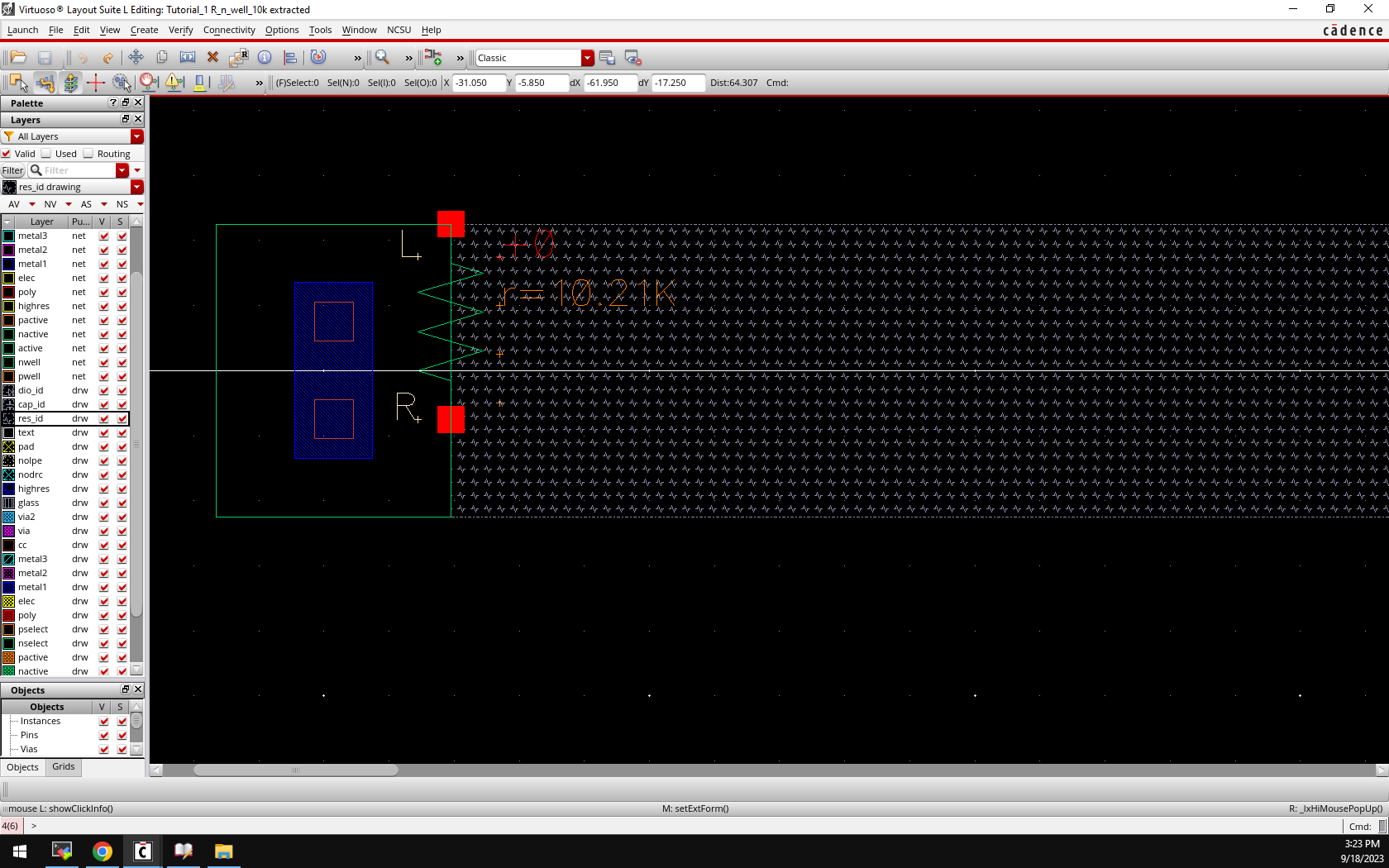
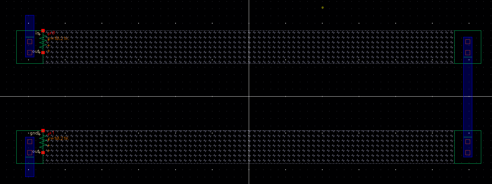
Now
that the layout is finished, we can DRC the layout one more time to
ensure there are no errors and extract to see the resistance of the
n_well. Below is the extracted view of my layout which shows my n_well
has a resistance of 10.21kOhms. This n_well resistor will be used to
generate my layout for my DAC in the lab report.
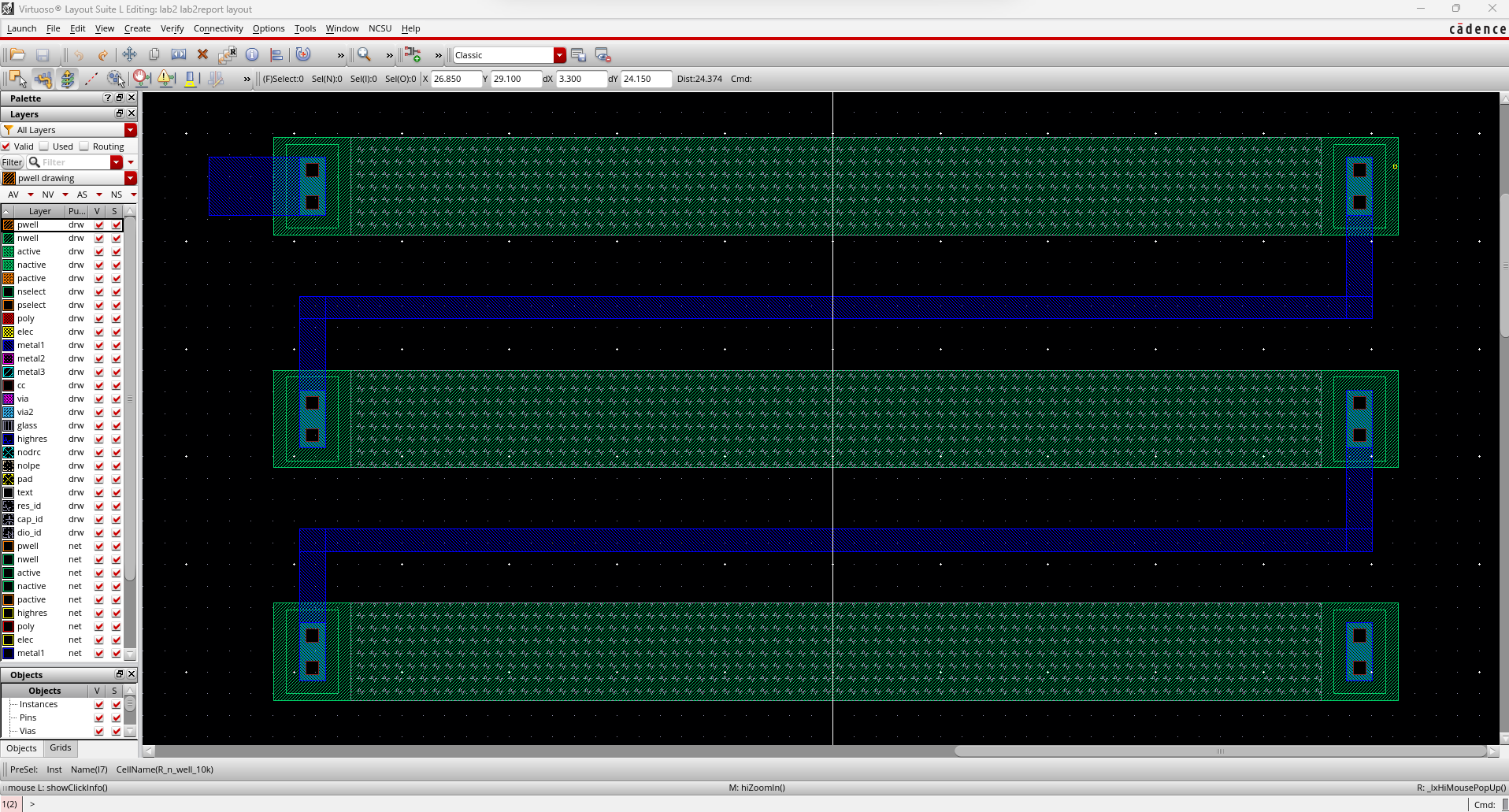
Next, I created a Layout Cell View for my Voltage Divider. I then built the follow layout using the 10k n_well resistor above.
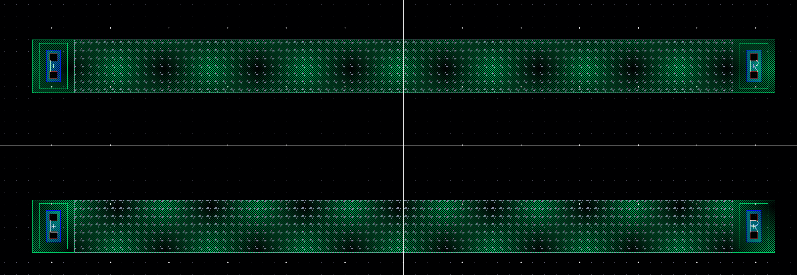
Next,
I connected my resistors using the metal1 layer. Then, I created pins
in the metal1 layer for in, out and gnd. It is important to make sure
to choose the proper I/O type for each pin. For example, in must be an
input pin and gnd must be an input/output pin. It is also important to
name the gnd pin as gnd!. The exclamation point indicates a global
value.
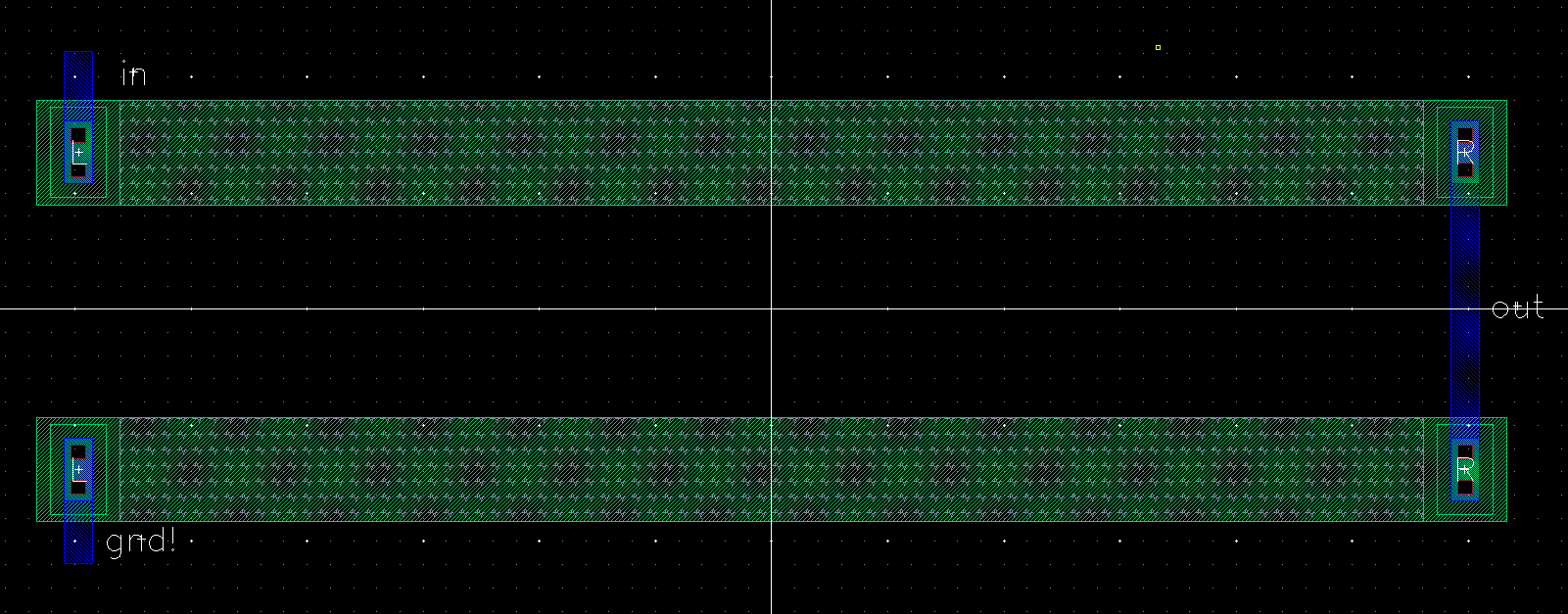
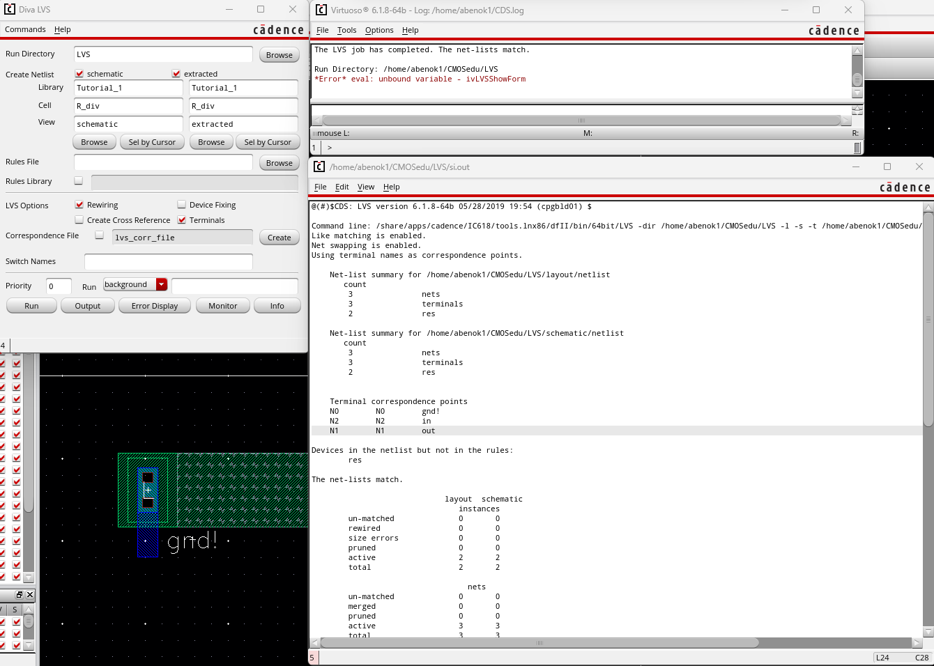
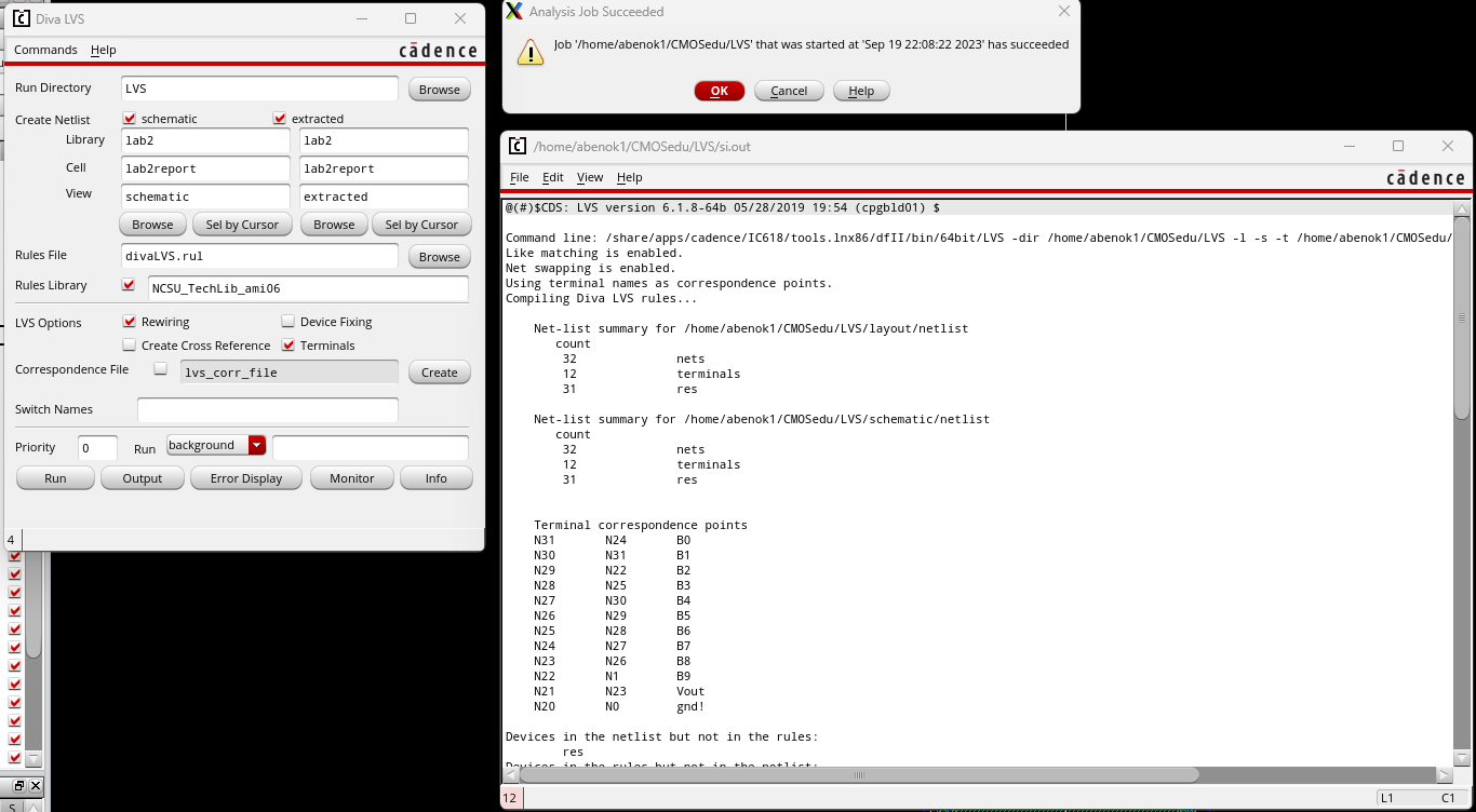
Lastly, I DRC'ed my design, extracted it and performed an LVS to ensure all of the netlists matched.
Lab Report:
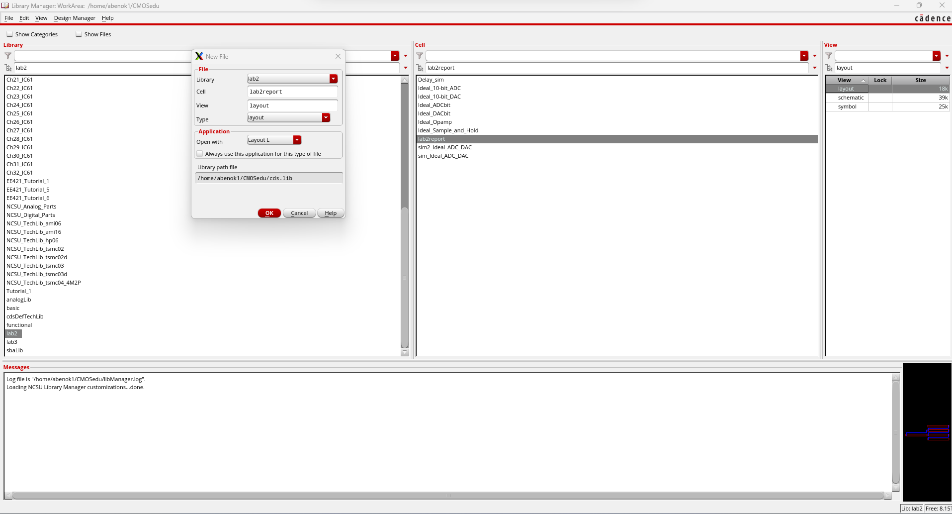
The first thing I do is create a layout cell view for my DAC schematic I made for Lab 2.
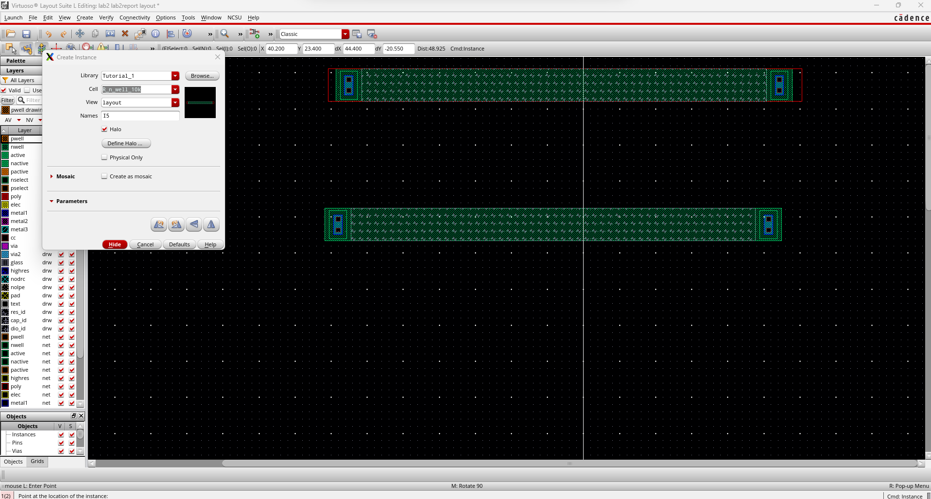
Next, I create a new instance of my 10k n_well resistor to start generating my layout.
If
I wanted to measure the length and width of my resistor, I can go into
the Tools tab and use the ruler to create measurements.
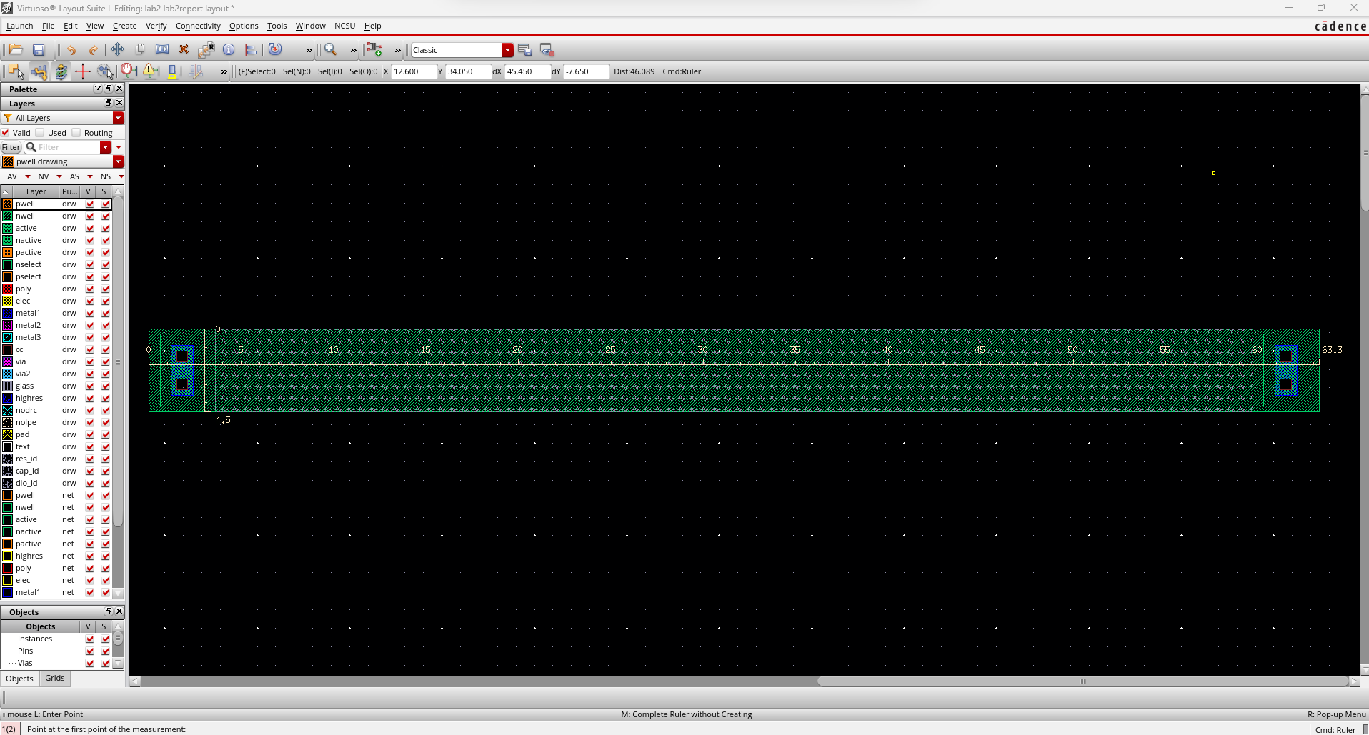
We can figure out what length
and
width to use by knowing what process we're using for our simulations.
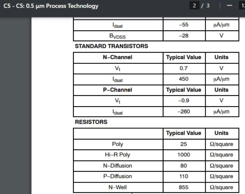
We are using the ON's C5 process which we can find the
data sheet for to see that the n_well layer has a rating of 855 ohms
per square. We chose a width of 4.5 microns, so we can figure out the
length we need for a 10k resistor by using the formula R = Rsq * (L/W).
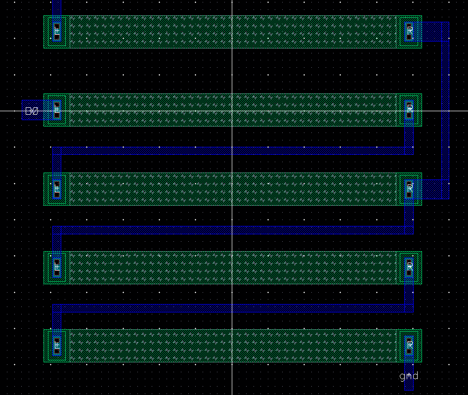
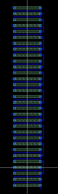
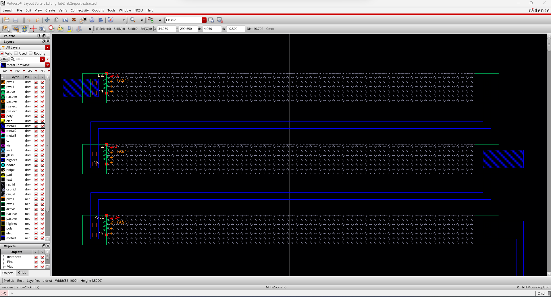
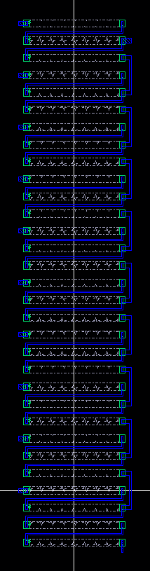
Since
the design of the DAC is modular with each bit, I create the circuit
for one bit, so I can copy and paste to make the process quicker. The
resistors will be connected by the metal1 layer. However, note the
least significant bit has an extra resistor at the bottom. It is also
important to DRC throughout this process to ensure no errors are
detected.
After generating all of the resistors and their
connections, I can now add the pins for bits 0-10, gnd and vout while
making sure to DRC throughout.
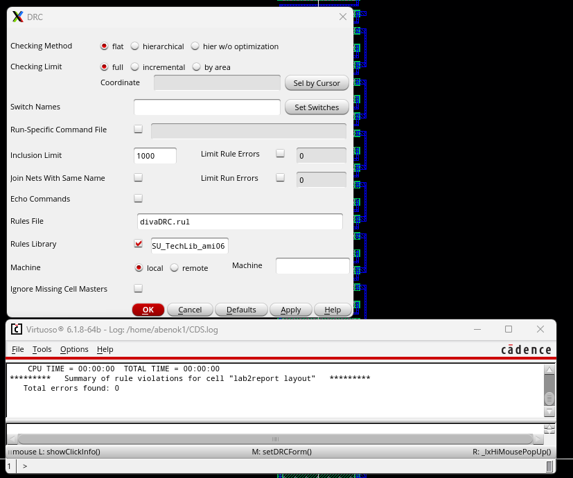
Below are my results after doing a final DRC,
extracting and lastly performing an LVS. All my files will be linked in
a zip file below.
Lab3 Zip
(Note,
it will download a zip file for lab2 since I built the layout from
Lab2. The Layout, Schematic and Extracted Cell View can be found in the Cell titled lab2report)
Return to 421L Labs