Lab 2 - ECE 421L
Authored
by Kyle Abenojar, abenok1@unlv.nevada.edu
September 13th, 2023
Prelab:
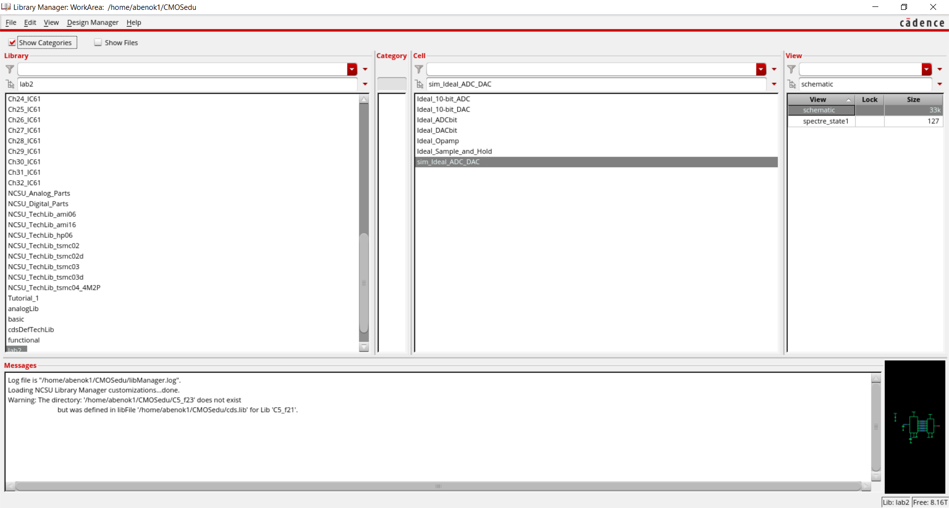
After
uploading the lab folder into my CMOSedu folder and editing the cdslib
file, I navigated to the folder in the Library Manager to open the
ideal_ADC_DAC schematic.
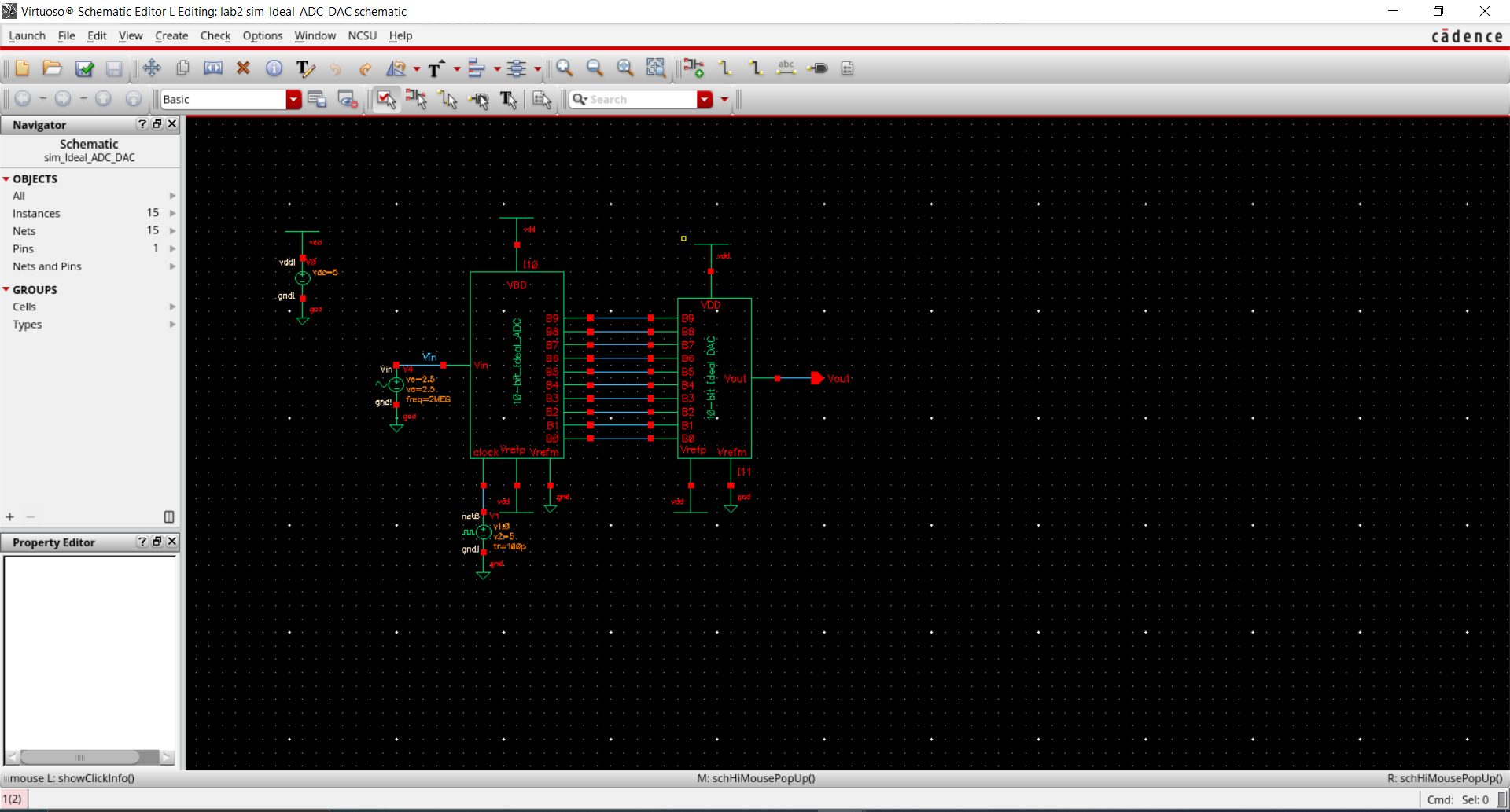
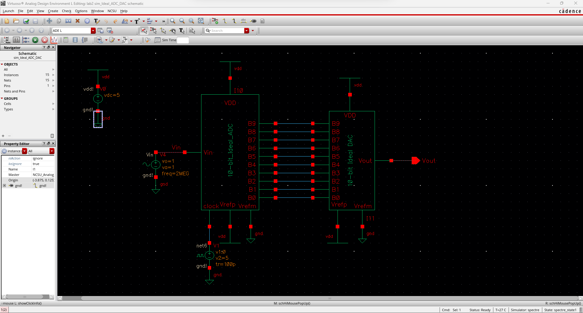
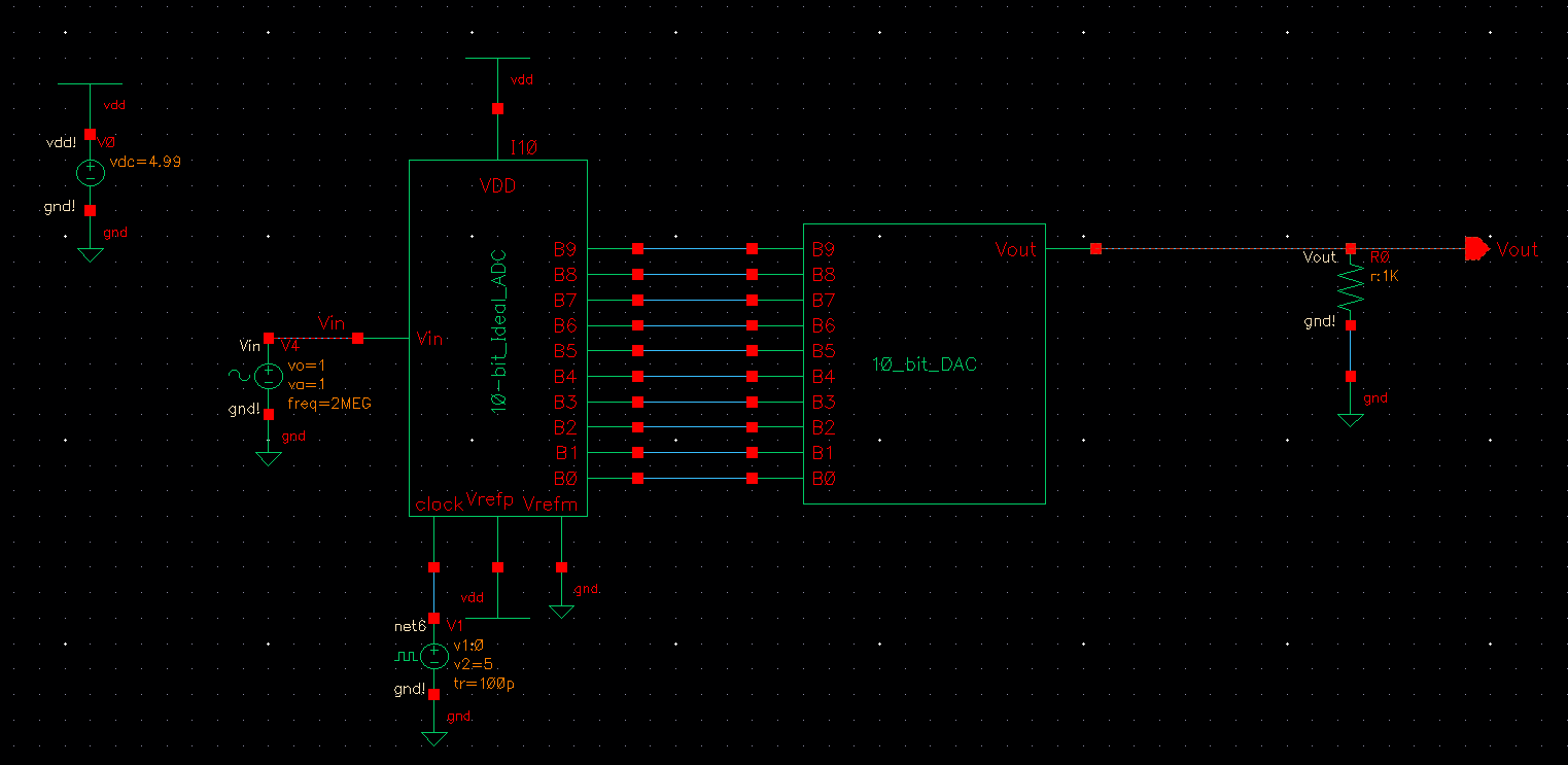
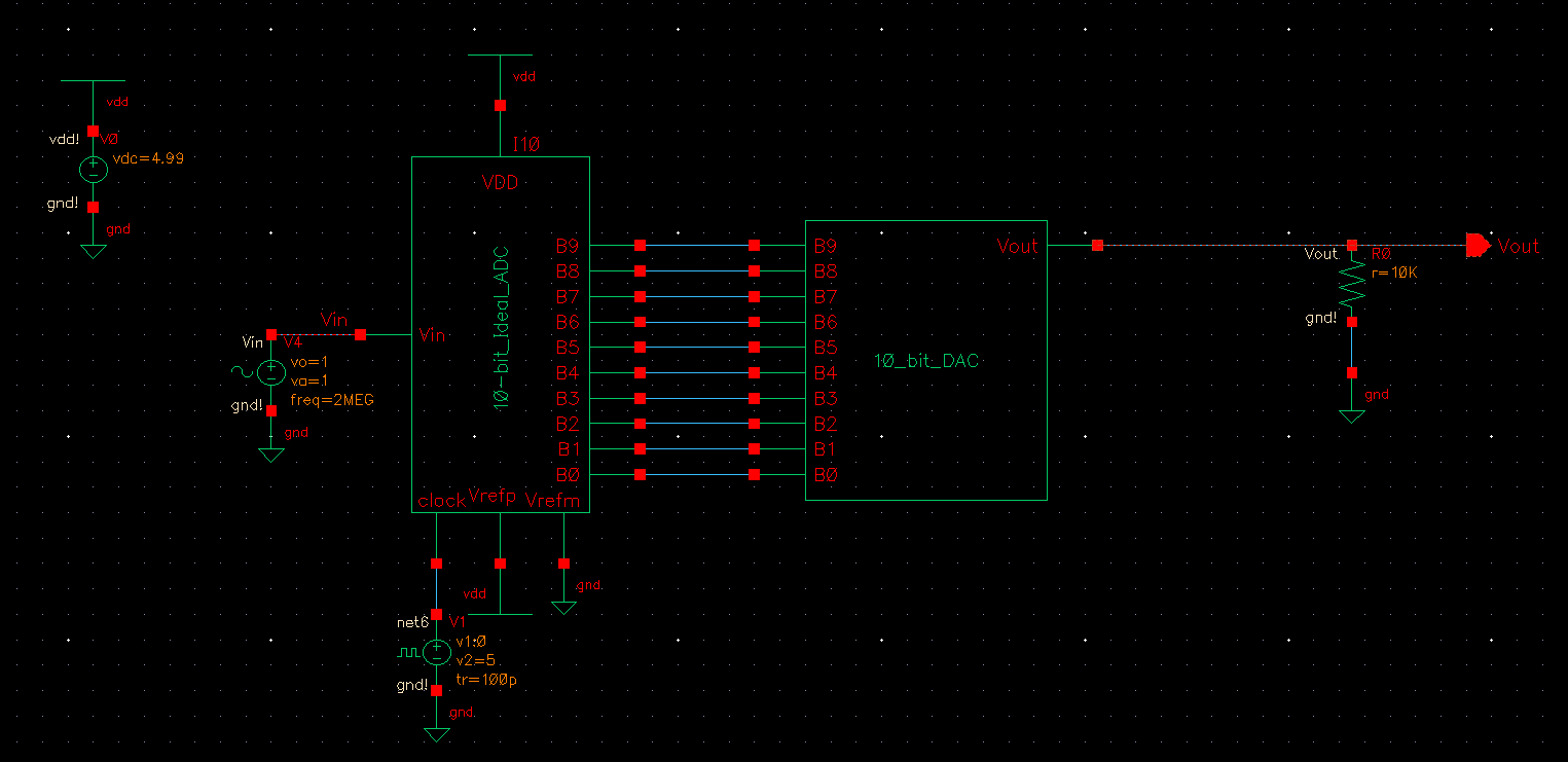
I
then launched the ADE, loaded up the previous state and ran the
simulation which gave me the graph below. As indicated by the schematic
above, we are taking an analog signal (Vin) and turning it into a
digital signal via the ADC (Analog to Digital Converter) module. This
module then feeds into a DAC (Digital to Analog Converter) which turn
the digital signal back into an analog signal which gives out Vout.
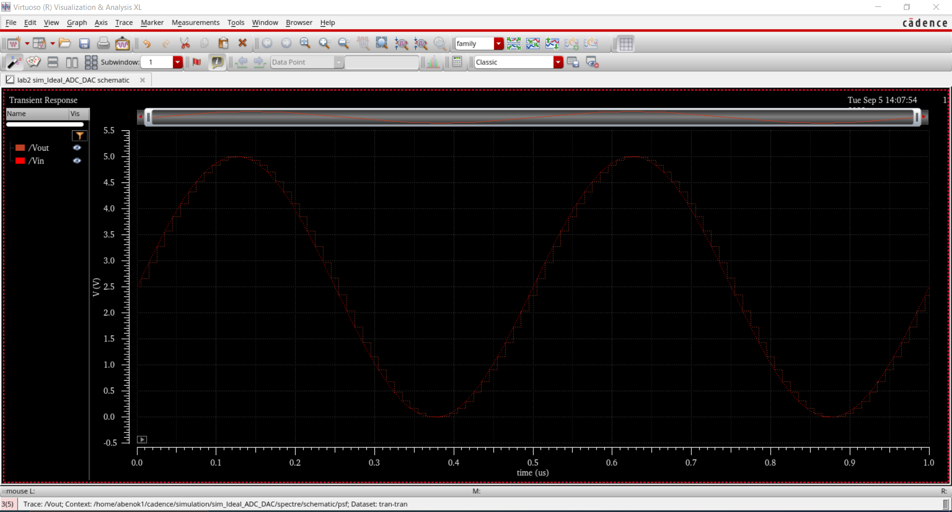
However, as shown in the graph below, Vout is not a perfect recreation
of Vin because the some of the original signal's data is lost due to
the ADC.
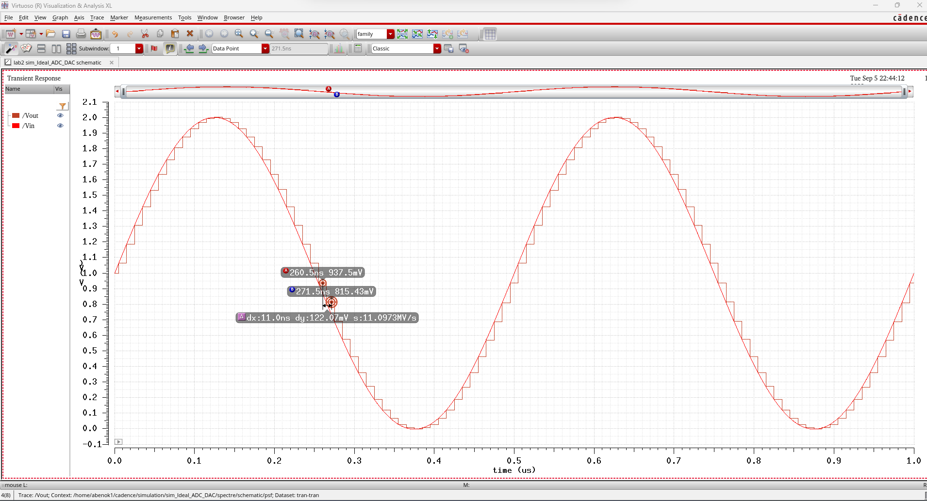
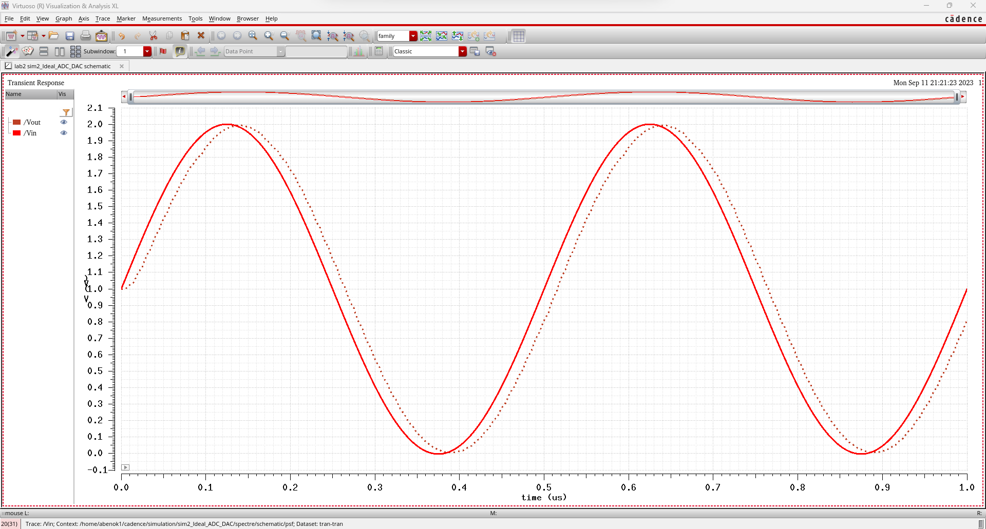
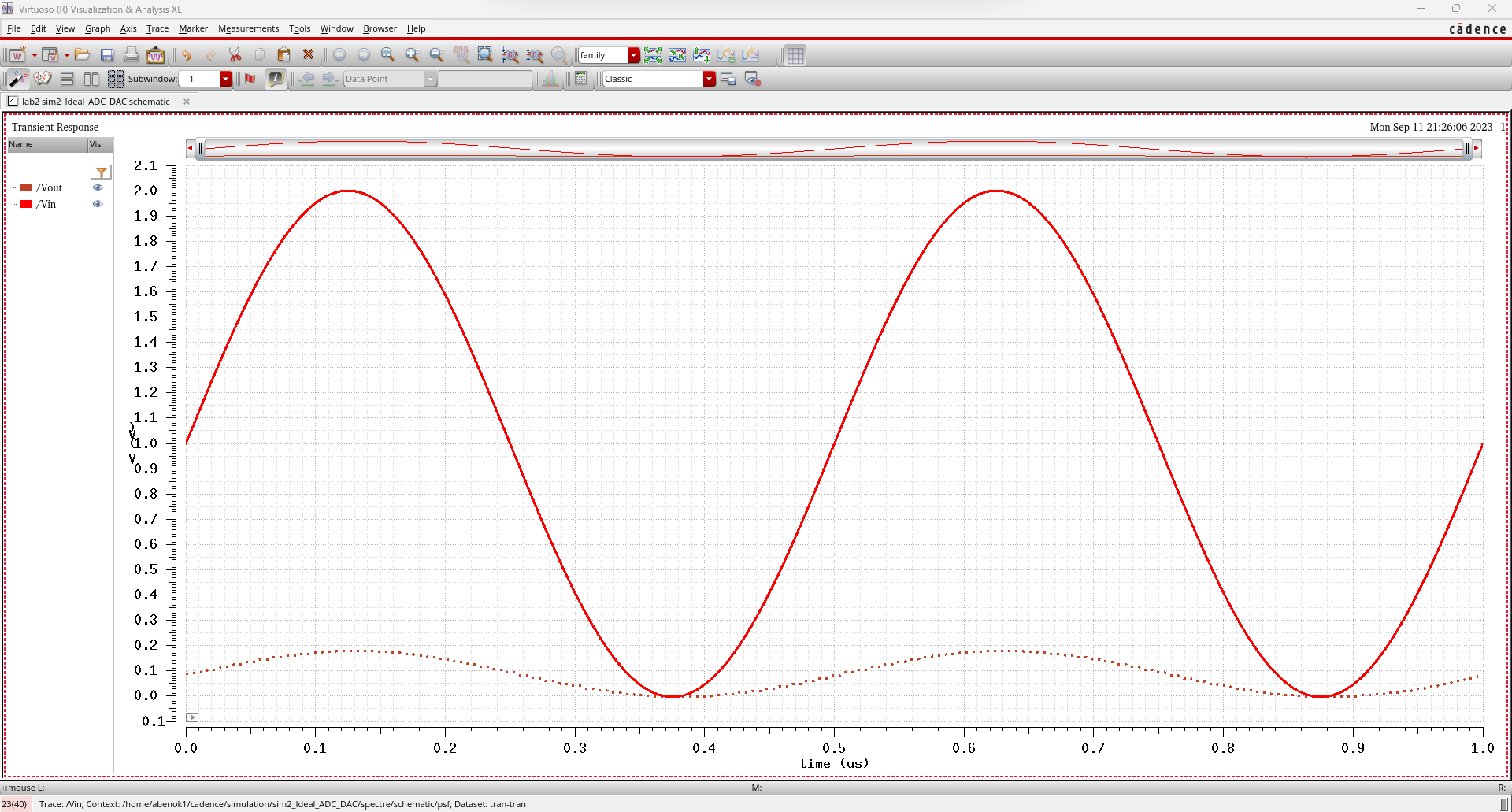
In
the picture below, I changed the amplitude and offset of the Vin
voltage source to 1V changing the range from 0 to 5V to 0 to 2V.
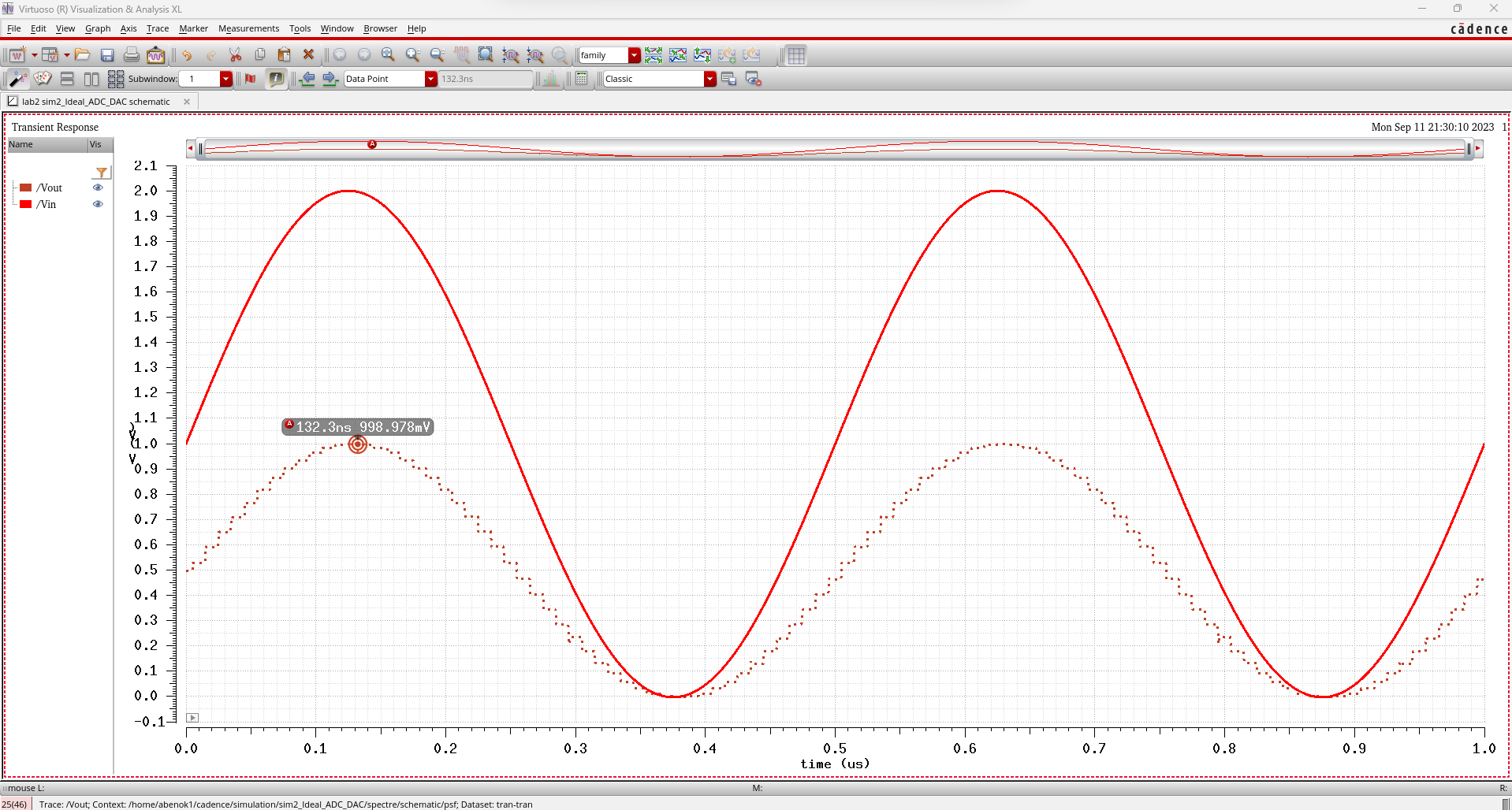
This
is how the simulation changed. Here we see again that the original
signal is partially recreated after going through the system. The
resolution of the system is limted by the number of bits that our DAC
can process. We can find the resolution of our system by taking the
reference voltage (2V) and dividing it by 2 to the power of n bits. In
this case, we would do 2V/(2^10) which gives us about 190mV which is
similar to the 122mV steps seen in the simulation below. We can
increase the resolution of our system by increasing the number of bits
or decreasing the reference voltage.
Lab Report:
Design:
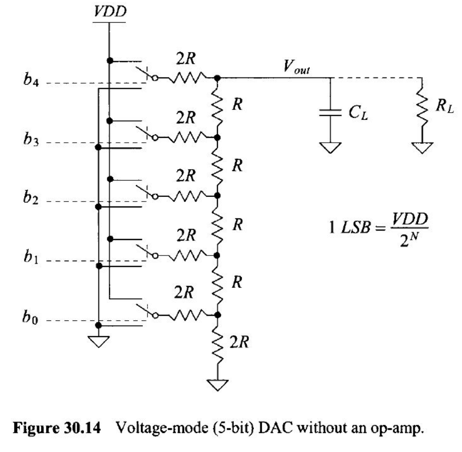
In
this lab, we were tasked with building and simulating a 10-bit DAC. The
figure below shows the general circuit that we will use to build our
DAC.
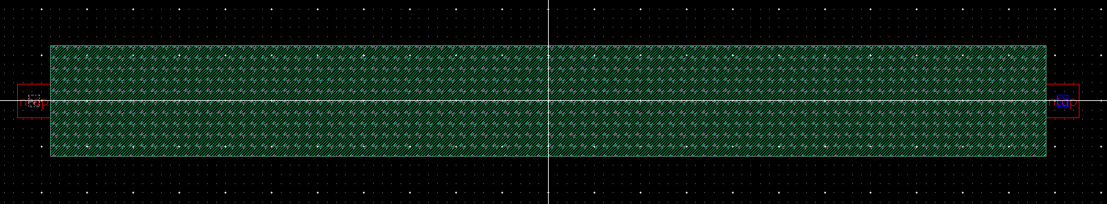
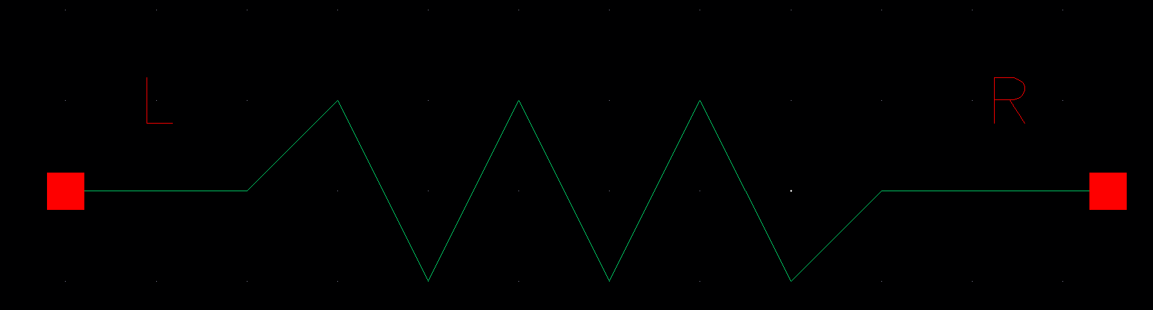
To start this lab, I built 10k n-well resistor which we will be using for our 10-bit DAC. The picture below is the layout view of the resistor.
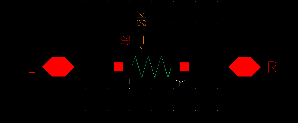
The picture below shows that schematic for my 10k n-well resistor.
Lastly,
below is the symbol view of my 10k n-well resistor. This will be the
symbol that will be used to build the DAC schematic.
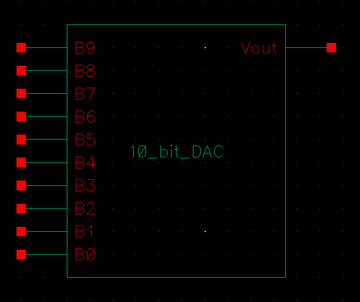
Next,
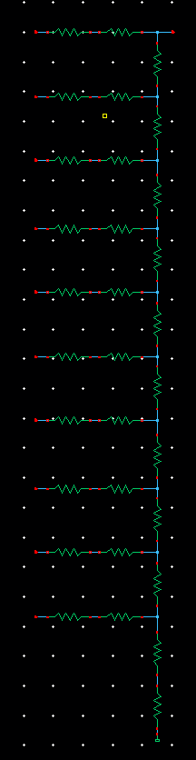
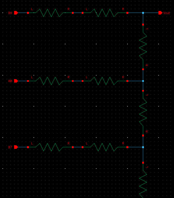
I built the schematic for my 10-bit DAC using my 10k n-well resistor.
The pictures below show the entire schematic as well as a zoomed in
view to give a better look at each bits' circuit.
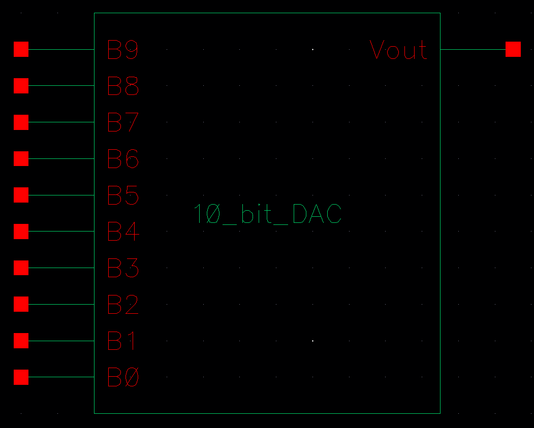
Here, I also made a symbol for my DAC. I will go over how to build this symbol further in the report.
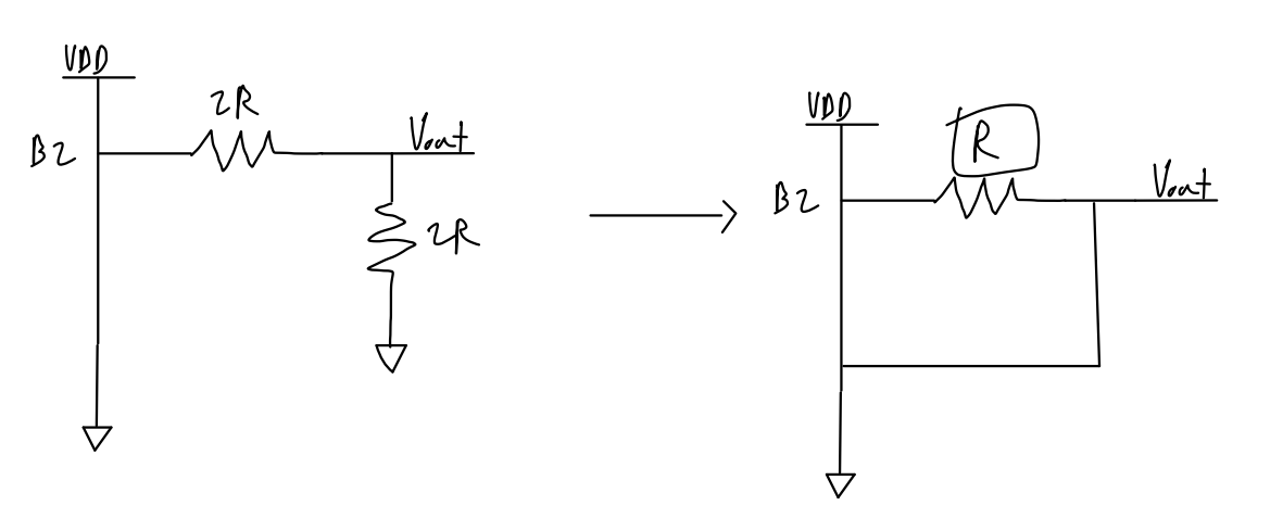
How to determine output resistance:
I
will use a smaller DAC to show the process of determining the output
resistance since the process will simply repeat multiple times.
To start, we combine the bottom two resistors in parallel. 2R || 2R = 1R. Next, we combine the bottom two resistors in series. 1R + 1R = 2R.
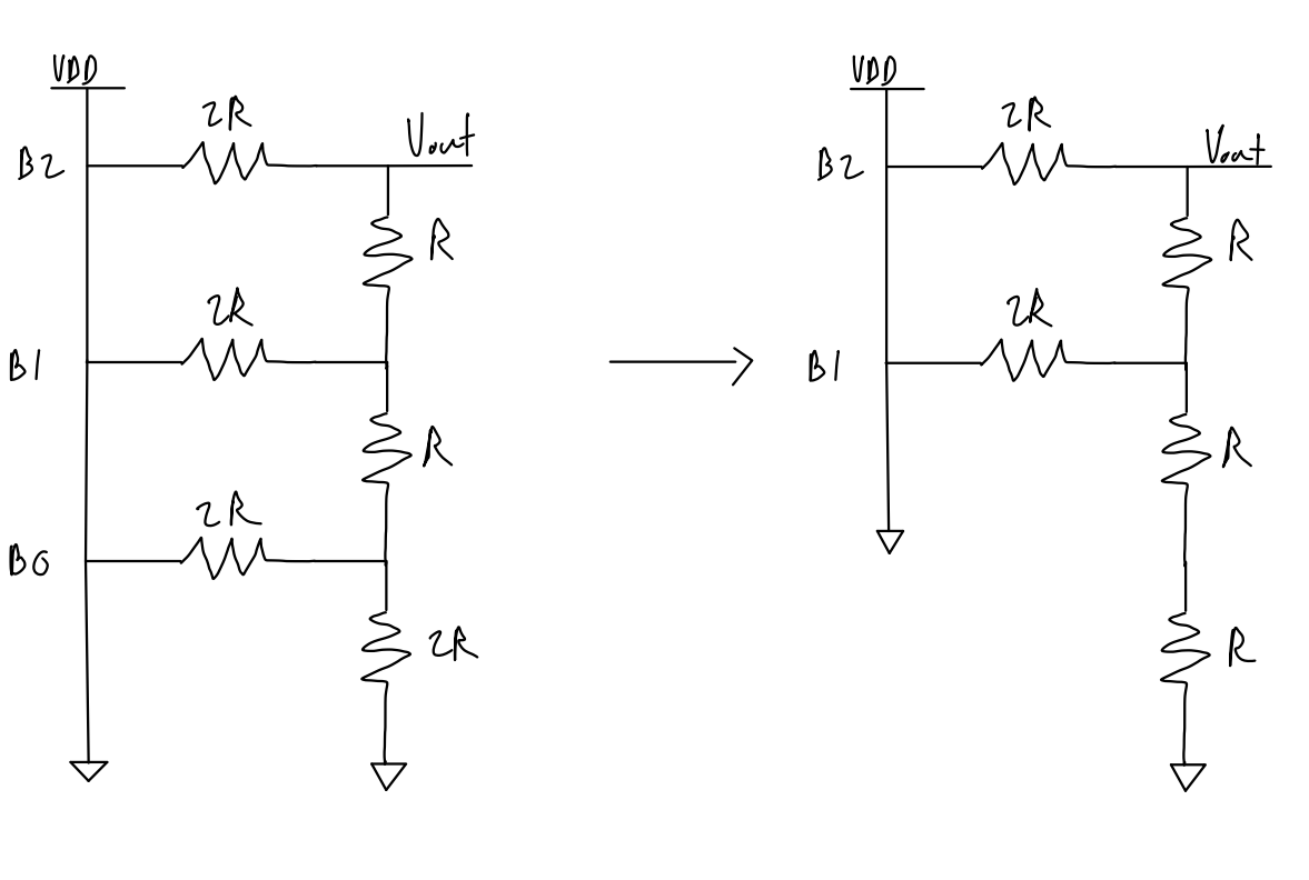
Then, we repeat the process of combining the bottom two resistors in parallel and combining the next two resistors in series.
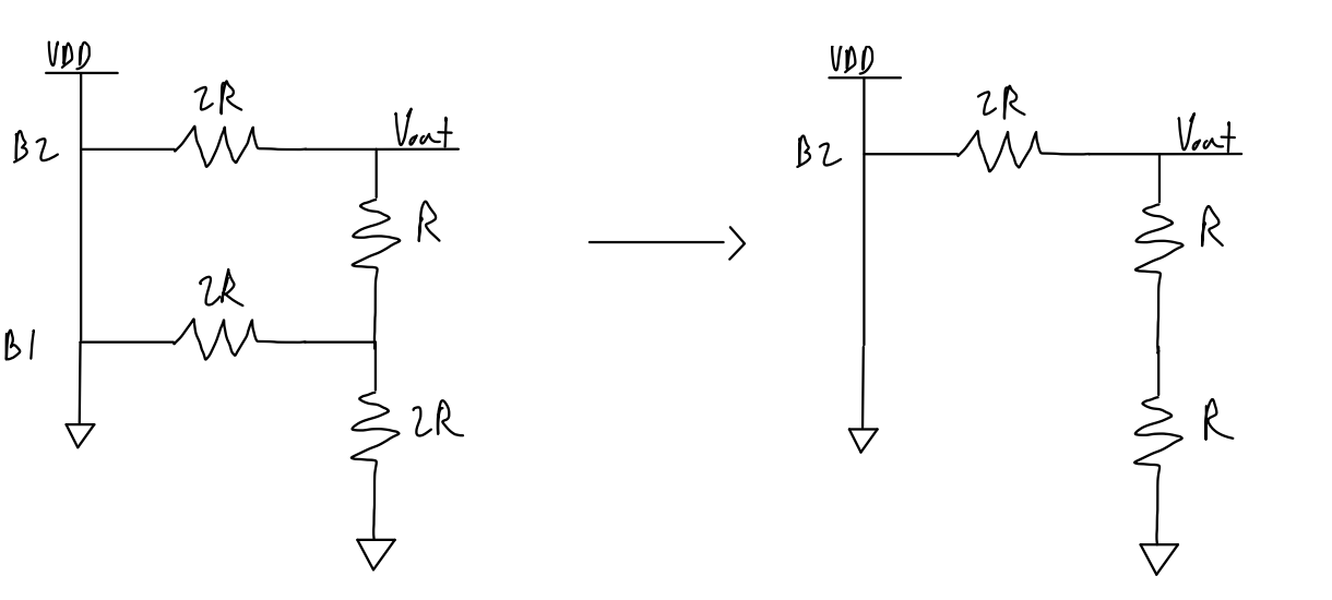
Eventually, once we reach the top, we find that the equivalent output resistance is 1R.
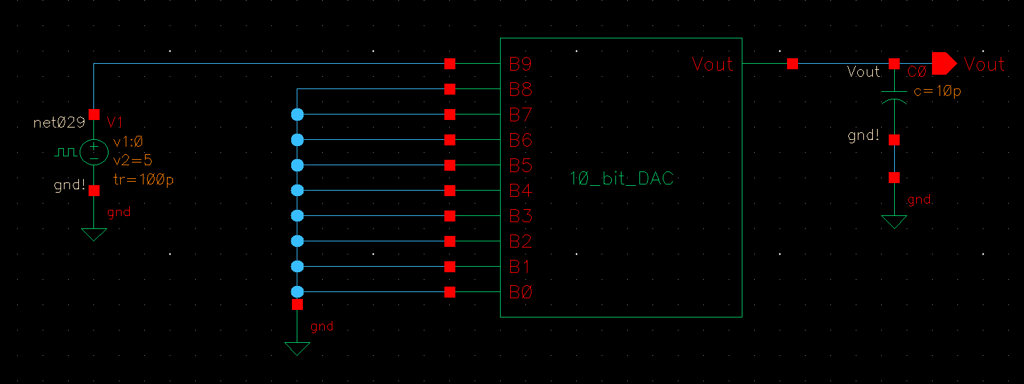
Delay, driving a load:
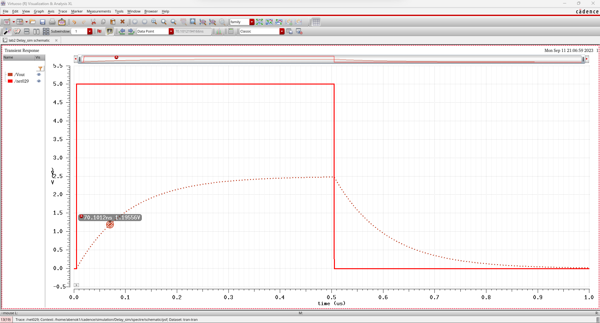
Next
I checked the delay of driving my DAC when there is a capacitive load
of 10pF. We can predict the delay using the formula 0.7RC which is the
time it takes to charge the voltage of the output to 50%.

To
simulate this, I grounded the inputs of my DAC and connected a pulse
source to B9. The pulse source goes from 0V to 5V (VDD). Below is the
schematic for my simulation.
Below
is the image of the output of my simulation. As we see, the peak of the
output is about 2.5V. At 70ns (0.7RC) we see that Vout is at about 1.20
V which is close to 50% of the maximum output voltage.
How to create a symbol view:
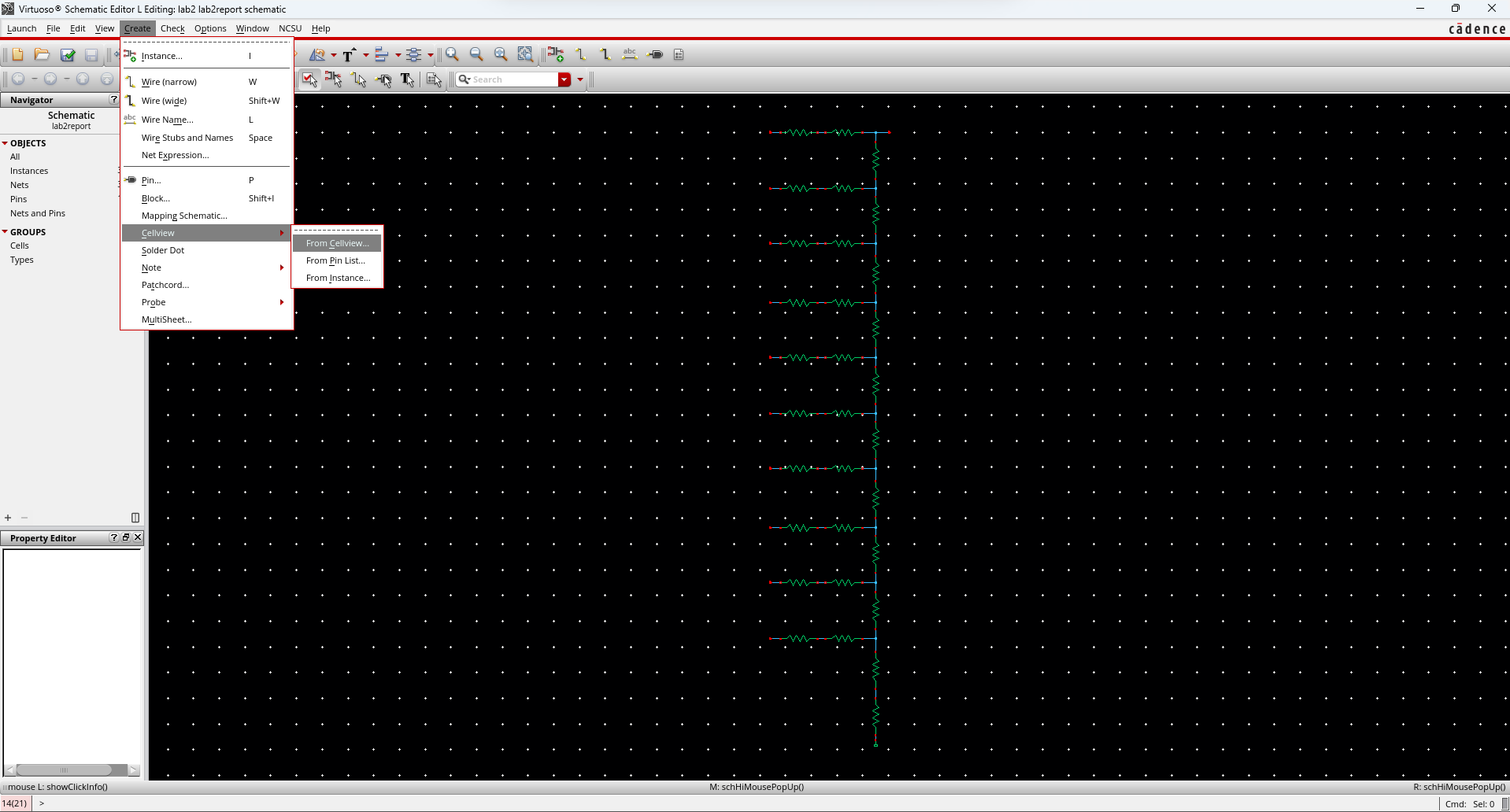
To start creating a symbol for my DAC we go to the Create tab and go to Cellview.
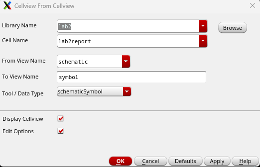
After
clicking this the following window should open which will allow us to
generate a symbol view for our schematic and to open the symbol editor.
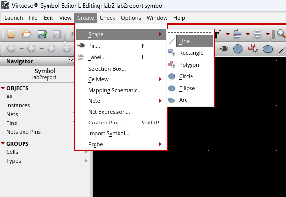
In the symbol editor I used the delete function and the line function shown below to form the following symbol for my DAC.
Simulations:
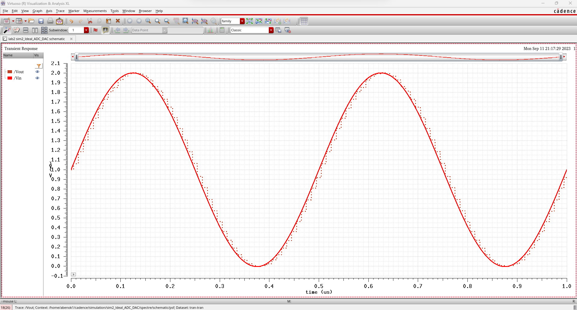
The first simulation that I performed was simply placing my DAC in place of the previous ideal 10 bit DAC used in the prelab.
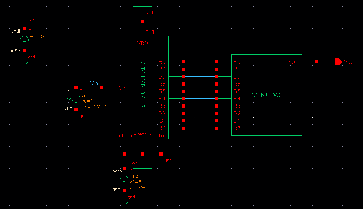
Here
we see that my DAC produces a similar output to the ideal DAC. Vout is
a jagged recreation of Vin. Again this is due to the limitation of the
DAC only being able to contain 10-bits of data. This means that some of
the data of Vin is lost during conversion of Vin to a digital signal
and back to an analog signal.
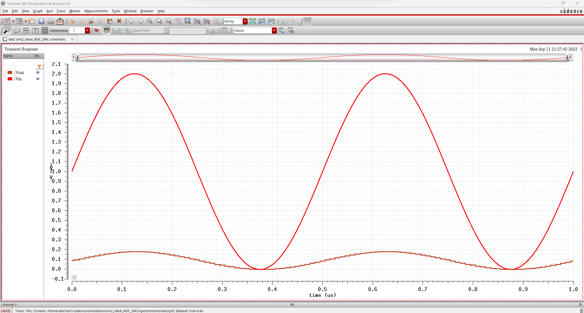
The next simulation involves a capacitive load of 1pF added to the DAC.
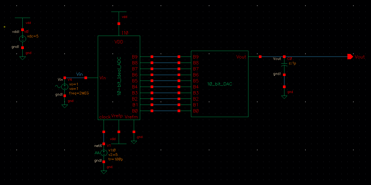
The
addition of the capacitive load creates a greater time delay between
Vout and Vin while also smoothing out Vout making it appear more
similar to the original signal.
The next simulation adds a resistive load of 1k to the DAC.
The
addition of the 1k resistor changes the peak voltage of Vout. This
creates a circuit similar to a voltage divider. Since the resistive
load is 1k and the output resistance is 10k (1R as shown above), the
output voltage should be about 1/11 of Vin which is confirmed as shown
below.
The next simulation adds both a resistive load of 1k and a capacitive load of 1pF.
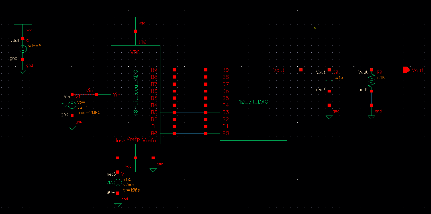
Here,
we see that adding a resistor and capacitor combine both of the effects
mentioned above. The resistor changes the peak output voltage and the
capacitor provides the signal smoothing.
The final simulation involves adding a 10k resistive load. Similar
to adding the 1k resistive load, we expect the circuit to act similar
to a voltage divider. This time since the resistive load is 10k, we
expect Vout to be halved (Vout = Vin * [1R / (1R + 1R)] = 1/2 Vin).
As expected, the output voltage at the peak is about 1V which is half of 2V.
What happens if the resistance of the switches aren't small when compared to R?
If this were to happen, the
output resistance of the DAC would be greater than R when simplified
similarly as shown above. A greater output resistance means that the
output voltage would be reduced.
Return to 421L Labs