University of Nevada Las Vegas. Department of Electrical and Computer Engineering
The 8-Bit, 32 Word Register File
Design, Analysis
and Implementation in the ONSEMI C5 Process
By Brian Wolak
Introduction / Theory of Operation

Description of Components
Each
8 bit memory cell of my design will follow closely with a
traditional SRAM memory architecture 6 transistor topology. The design
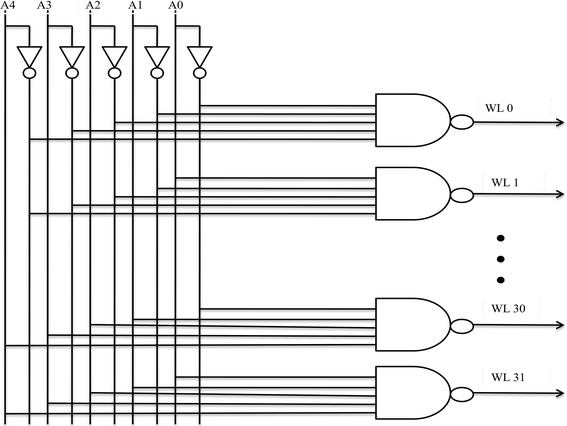
will also involve a 5-bit address input to allow access to each of the
32 8-bit word registers. This input address will be accessed through
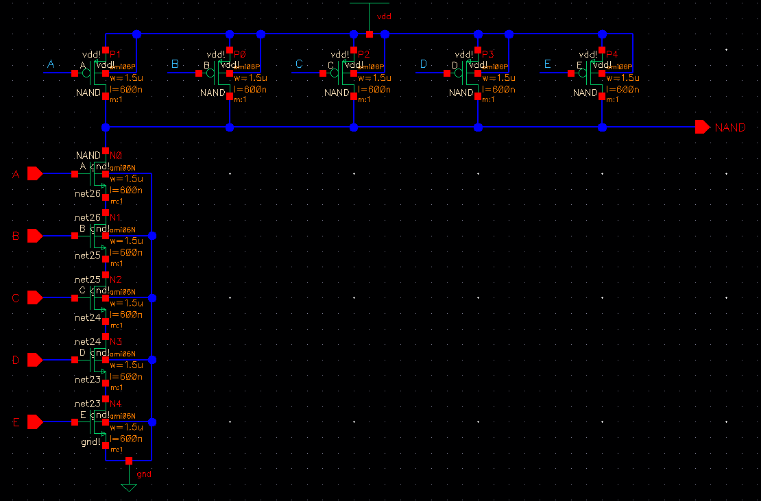
the use of a 5:32 row decoder designed using 32 individual 5-bit input NAND gates.
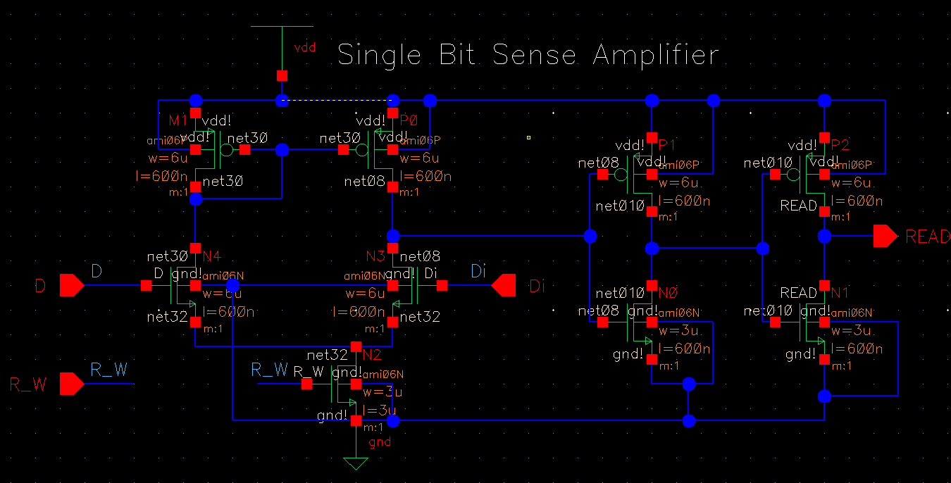
The read/write portion of my design will involve a sense amplifier
designed to read each bit line and sense voltage difference on a read
cycle which is separated from the write portion of the circuit. Because
this design does not involve any clocked circuitry it remains
advantageous in it's simplicity and extremely low power
consumption.
The Single Bit Memory Cell
Beginning
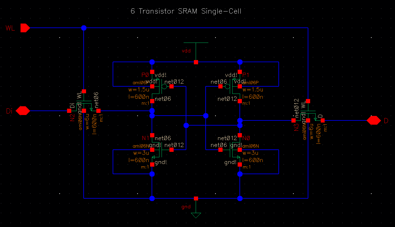
with a single bit of memory storage a 6 transistor (6T) individual
memory
cell was designed to retain one bit of data. In this topology, as long
as the circuit remains powered, data is saved. No refresh is needed as
the the circuit shown below
shows input/output bit line access using D and Di pins. The WL or word
line input is used to turn the cell on or off allowing stored data to
reach or be stored through the bit lines during read and write cycles.
6 Transitor Single Memory Cell Circuit
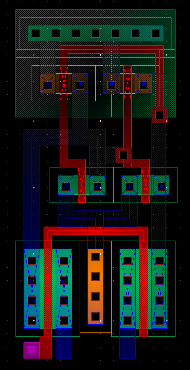
While
SRAM memory is inherently designed to be compact and efficient with the
purpose of saving costly chip space, I spent a lot of time assuring my
design would be as tight as possible to yield a extremely compact overall
layout design. Keeping the internal transistors at a minimum size, I
chose larger sizes to drive the bit lines allowing them to overpower
the internal transistors when performing a write operation. Below is
the layout of a single 6 transistor memory cell
used in my register file design.
6 Transistor Memory Cell Layout
The 8-Bit Memory "Word"
8-Bit Memory Word Cell Circuit
Combining the single bit cell designed above we use 8 individual memory cells to form an 8-bit word. This will be used 32 times in the register file design and will take the largest portion of layout space. The word lines of each single bit cell will be combined to allow access to all 8 memory cells with one input single, while each cell's bit lines will remain individual allowing individual memory to be stored uniquely in each cell. Shown below is the 8-bit word layout used in my register file design. Standard cell formatting was used to allow the design to remain expandable while maximizing the layout space.
5:32 Row Decoder
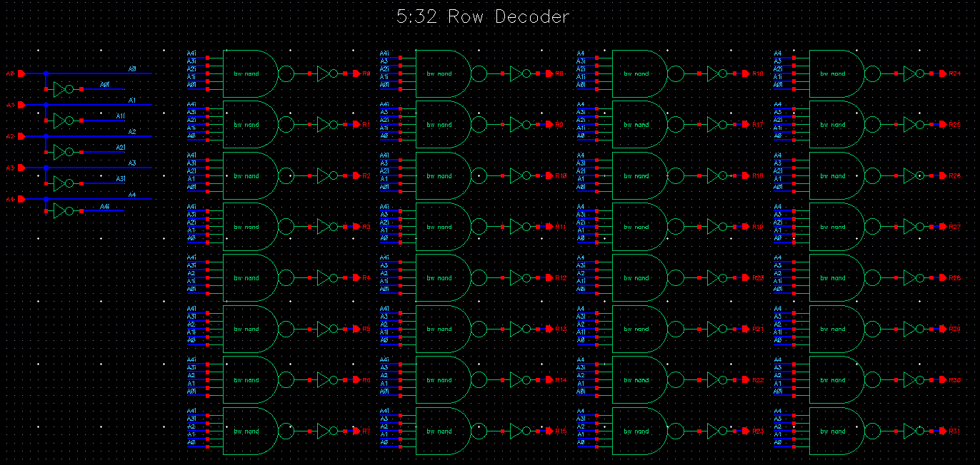
Row Decoder Schematic
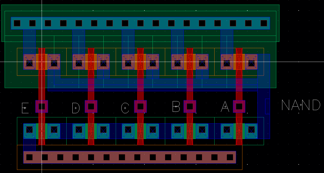
5 Input NAND Gate Circuit
5 Input NAND Gate Layout
Combining
32 NAND gates together along with an inverter to each word line, will form the overall decoder device.
Below we can see the 5:32 decoder overall schematic using the NAND gate symbol created in Cadence and the associated
row decoder truth table.
5:32 Row Decoder and Associated Truth Table
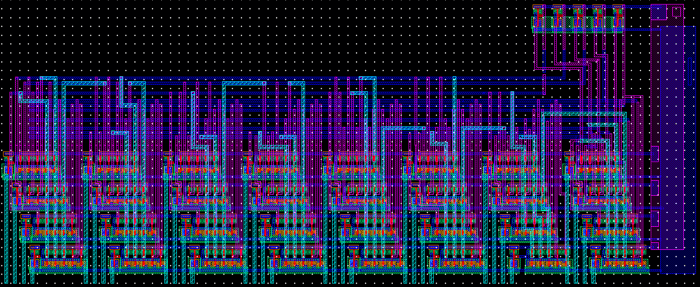
5:32 Row Decoder Layout
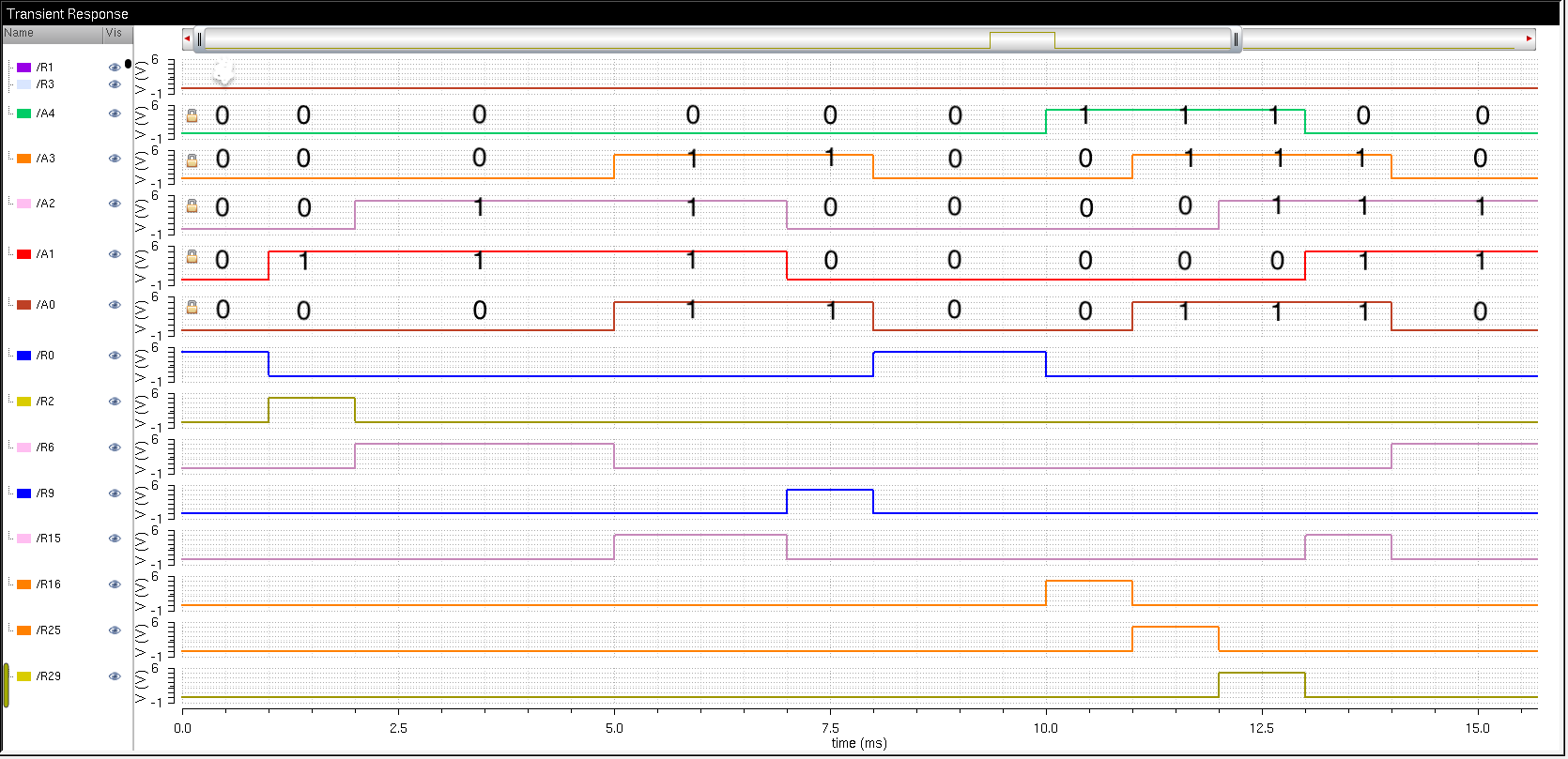
Running a simulation to verify operation of the row decoder we achieve the output shown below. We can see that when comparing the truth table to each A[0:4] selection input the proper word line output goes high accordingly meaning each 8-bit word line would turn on the driver transistors making the 8-bit cell active for a read or write sequence.
5:32 Row Decoder Simulation Results
Single Bit Differential Amplifier
Single Bit Sense Amplifier
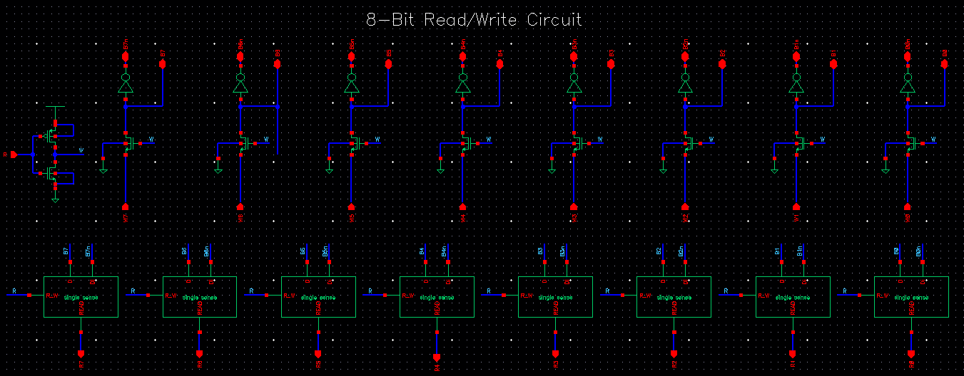
Read/Write Circuit
8-Bit Read/Write Schematic
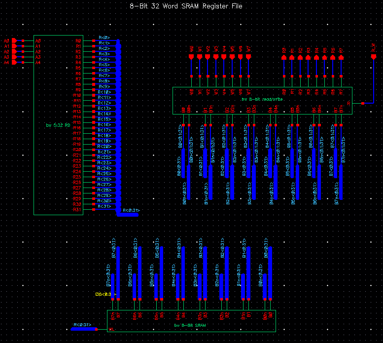
The Register File Assembled
Once
all these components were individually designed laid out and tested for design
rule compatibility using DRC and LVS checks, they were combined together to
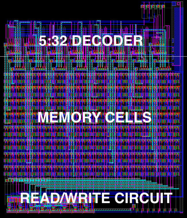
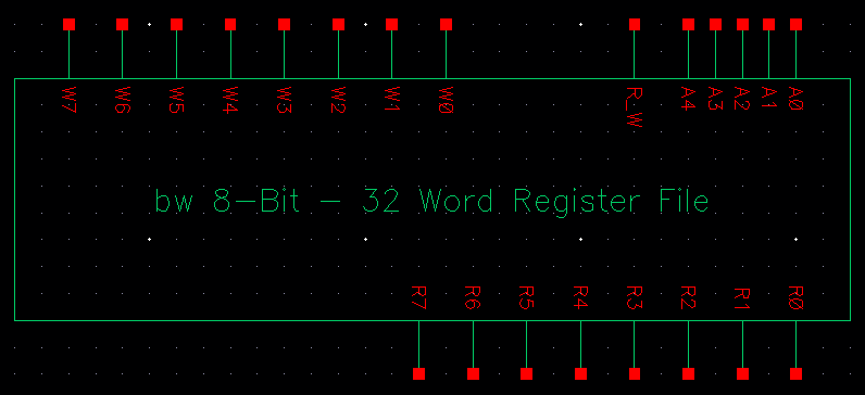
form the final product. Below are the final schematic,
layout, symbol and extracted views.
Final Symbol View
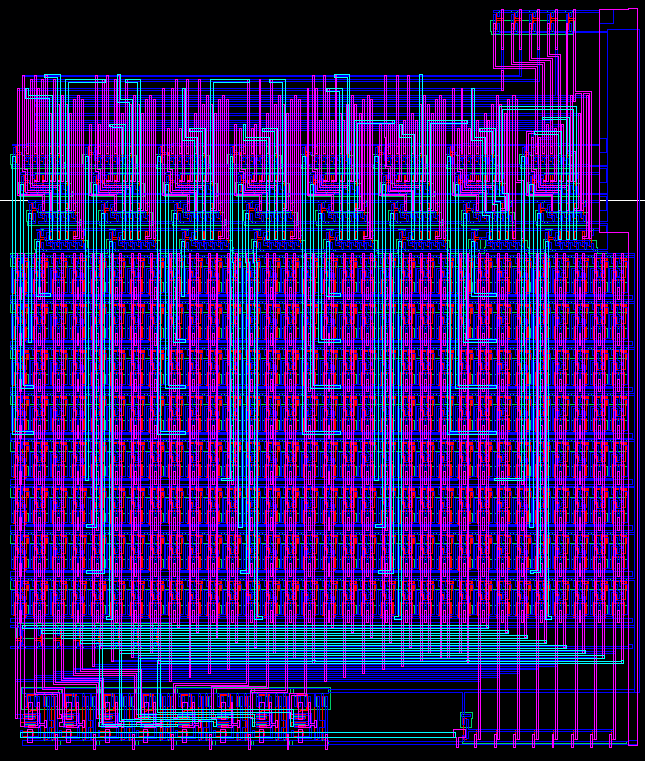
Final Master Layout
Final Extracted View

Final DRC and LVS Confirmation
Simulation and Testing
The
final design will now be simulated using different address inputs to
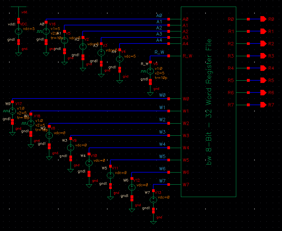
verfiy proper read and write functionality. In each of the following
simulations I will manipulate a small number of address bits to change
between multiple addresses while manipulating the write bits to write
multiple bit sequence of data to the addresses. Below is the simulation
schematic and results with explanation of each.
Simulation Circuit Design using
Project Symbol
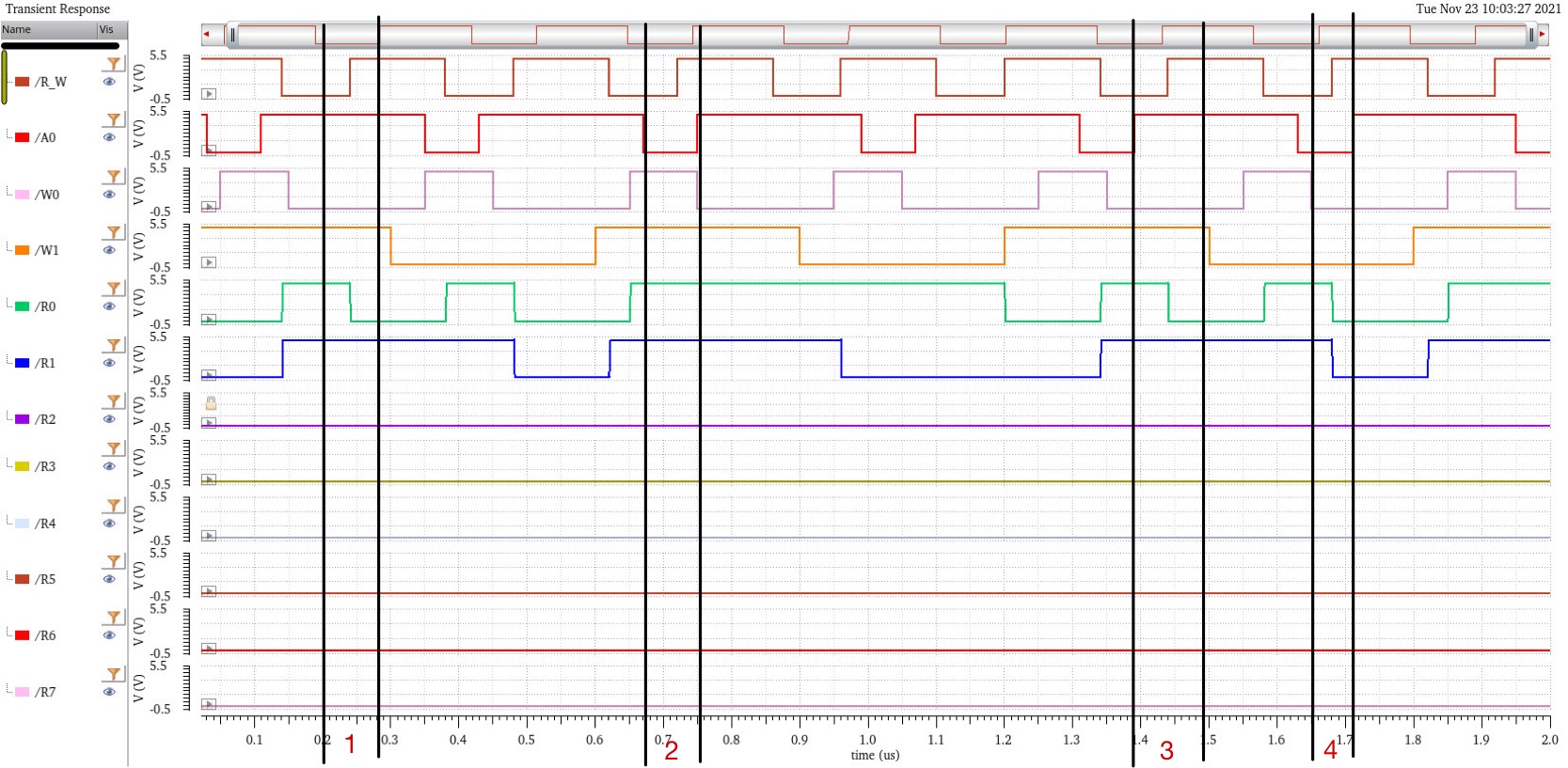
Simulation Results #1

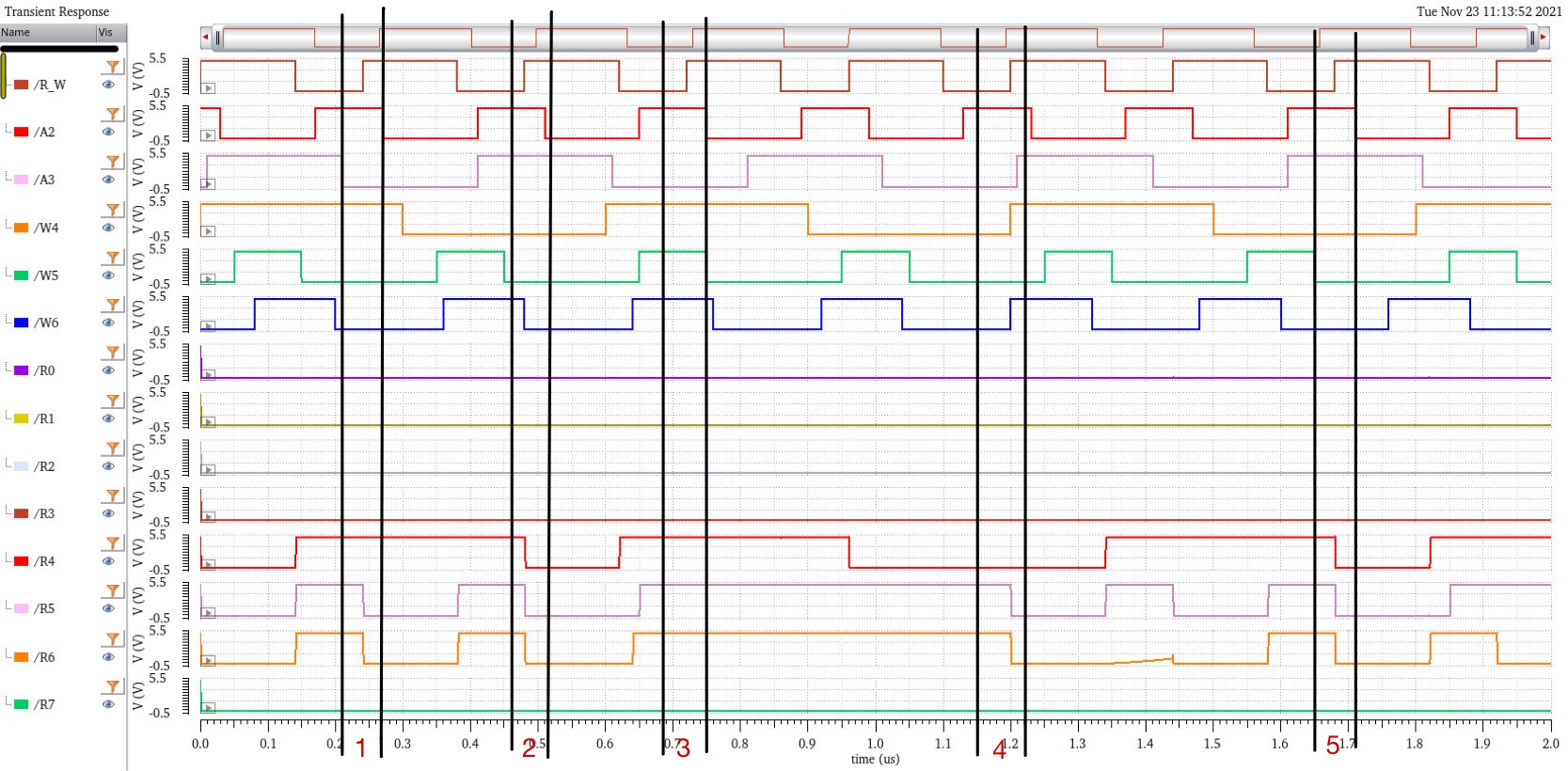
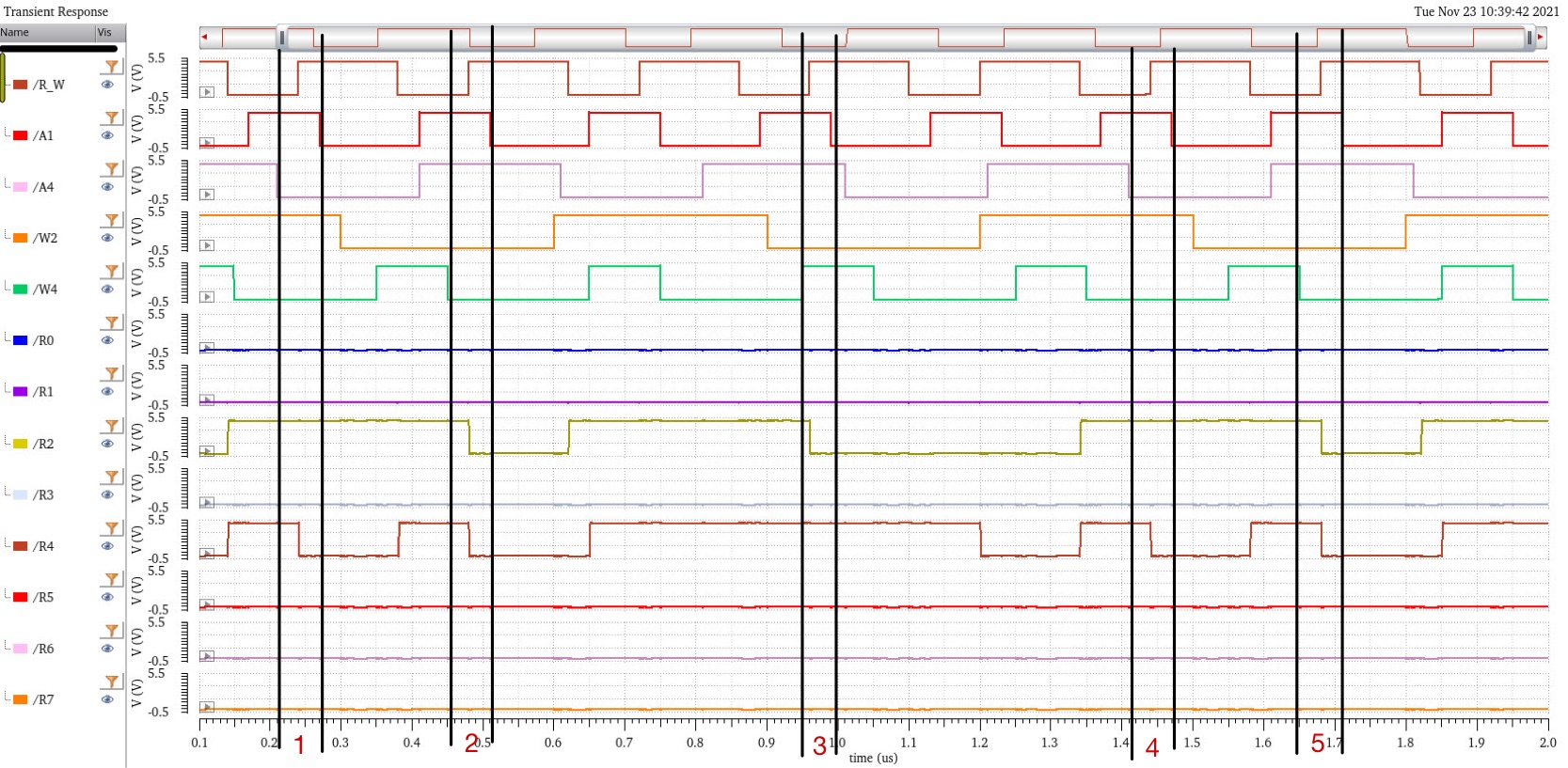
In simulation #1 we manipulate the A[2] input bit and can see that we are writing to register address 27 and 31 decimal values of 0, 16 and 112. Each read/write sequence returns the proper written value and functions as expected.
Simulation #2Simulation #2 Results

In simulation #2 we manipulate the A[3] input bit and can see that we are writing to register address 23 and 31 decimal values of 0, 4 and 16. Each read/write sequence returns the proper written value and functions as expected.
Simulation #3
Simulation #3 Results

In simulation #3 we manipulate the A[0] input bit and can see that we are writing to register address 30 and 31 decimal values of 0, 2 and 3. Each read/write sequence returns the proper written value and functions as expected.
Further Analysis
Analyzing the power consumed by my device over a single simulation I took the average amperage provided by the 5v VDD source and found it to provide an average of 367.9uA at 5v. Using the formula below with an average current value found through simulating I determined the average power consumption to be relatively low as expected for a static RAM device.

Using another method with the Cadence Virtuoso Calculator and the following function line I determined another value of 2.53mW for average power consumption.


Operating my device using a read/write period of 240ns gives a 4.16 MHz operating frequency. I did not test the device at higher operating frequnecy but further simulation testing could be performed to confirm at upper and lower end limit of operation frequency to avoid data corruption faults.
Conclusion
All design files, layouts, schematics and associated simulations can be found in the .zip file attached below.
proj_f21.zip
