Lab 7 - ECE 421L
Authored
by Michael Velasquez
velasm4@unlv.nevada.edu
October 20, 2021
Lab
description
Using buses and arrays in the design of word inverters, muxes, and high–speed adders
Prelab Content
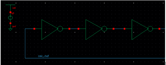
The
prelab had students design, layout and simulate a ring oscillator using
the NOT gates designed in a previous lab. A ring oscillator
continuously inverts the signal between NOT gates as long as there is
an odd number. Below shows a portion of the schematic, the full design
contains 31 gates and cannot be shown fully.
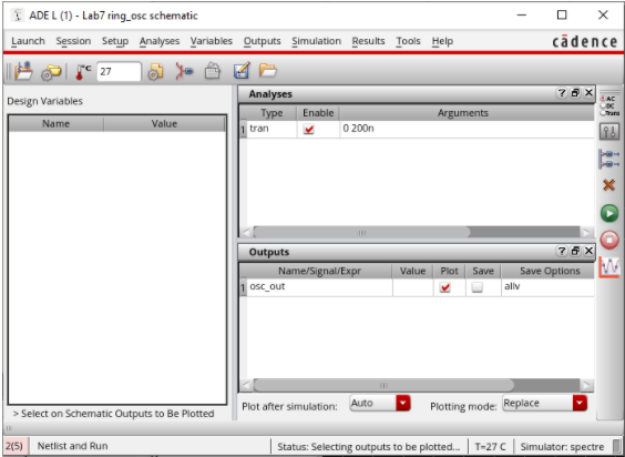
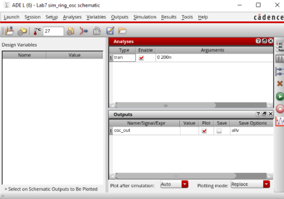
After the schematic was finished, students were to simulate. The ADE and simulation settings are as shown below.
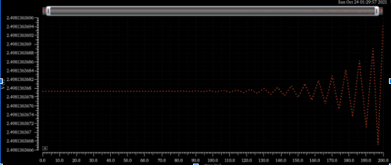
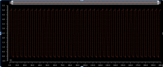
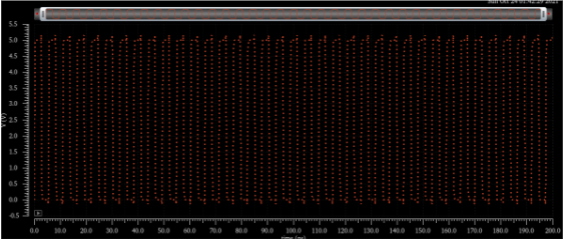
The
output of the oscillator is not as expected. This output shows a signal
that continously bounces around 2.5V. This is because no initial value
has been assigned, and it would take some time for the oscillator to
get started. In real circuits there is noise in any setting that can
jumpstart the oscillation.
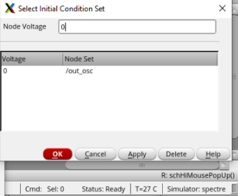
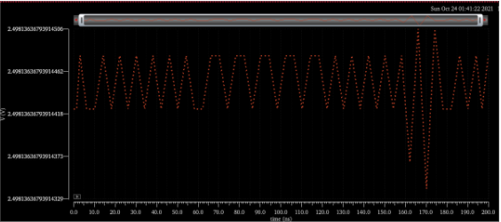
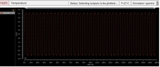
To
fix this issue, we set an initial condition to our output note in the
ADE. For this example we set the node to a voltage of 0.
As you can see, the new simulation shows the intended results. This leaves the output bouncing from 0 to VDD continuously.
Having
a large amount of the same instances in a schematic leaves the design
crowded and hard to follow. In order to make everything more neat,
students were to use busses (or wide wires) to create a schematic with
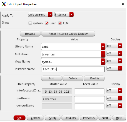
the same function as seen before but with a single gate. Labeling the gate using a notation such as I0<N-1:0> allows for the same gate to be present N number of times while only being placed once.
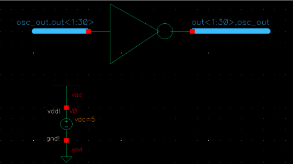
In this example we need 31 gates, so we change the instance name to represent this.
Once simulated, this new schematic still has the issue of not starting up. The same method was used to rectify this.
After the issue was fixed, the simulation showed the exact same results as the previous schematic.
Next
step is to layout the ring oscillator. To start, a single NOT gate was
created so the students can instantiate it N number of times.
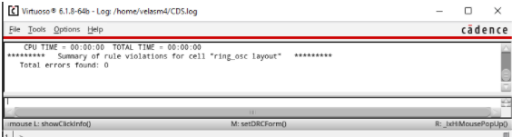
The layout was DRC clean.
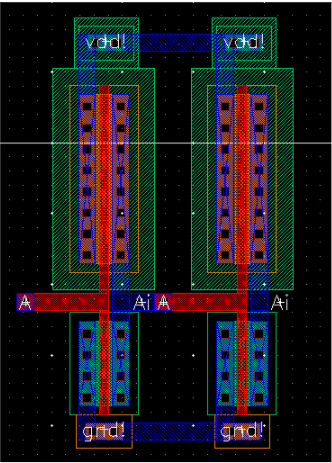
Shown
below is the array of NOT gates that was copied. This layout represents
both schematics that were created earlier in the prelab.
 .
.
Layout was DRC clean.
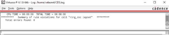
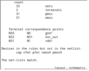
Students
were expected to LVS check the layout. This compares the layout with
the original schematic to ensure any nets, instances or terminals match.
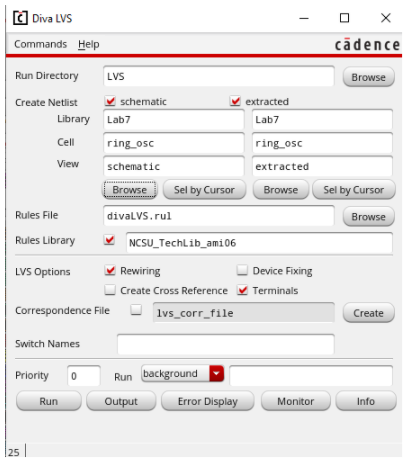
Layout was LVS clean.
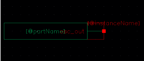
A symbol was created for this ring oscillator, with the only pin being the 31st output.
The test schematic for the ring oscillator is as shown below.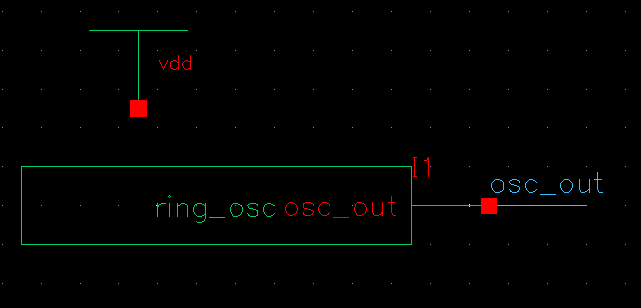
The ADE and simulation settings match what was used in previous schematics.
The simulation results are exactly the same, which match expectations.
This marks the end of the prelab content.
Lab Content
Lab 7 continues on the usage of busses and arrays to create functional and neat schematics.
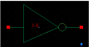
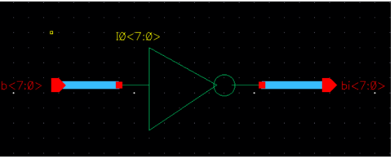
To start off, students were expected to design a four bit inverter.
This circuit takes four inputs and inverts them bit by bit. For four
bits, students were to change the instance name to I0<3:0> and
label the input and output nodes approprately.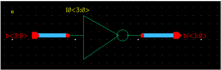
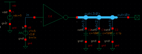
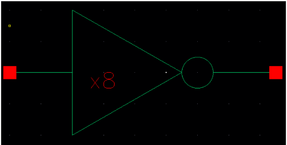
A symbol was created to show that this inverter is used for four input bits.
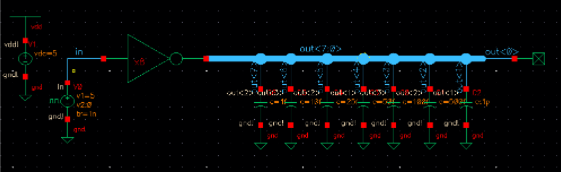
To test functionality a new schematic was created which includes an input source and a load for each bit.
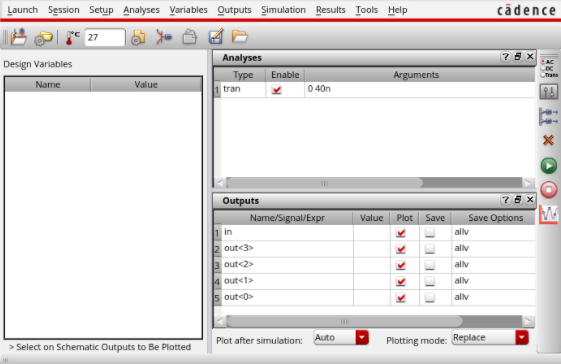
The ADE and simulation settings for the test schematic are as shown below.
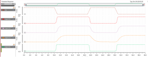
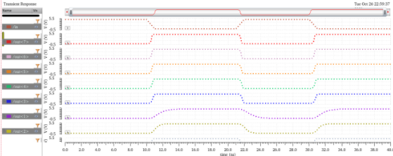
The results for the four bit inverter are as expected. As you can
see, the value of the load capacitor have an effect on the output
voltage at any given time. The larger the capacitance, the longer it
takeks for the inverter to charge it. For the fourth and first bit, the
output is simillar as the load capacitance for the third bit is
neglible. The larger the capacitance the larger the time constant which
leads to more of a curve in the output voltage.
After the four bit inverter was completed, students moved onto an eight
bit converter. The notation and design are very similar to the four bit
inverter shown above. Instance names and node labels were adjusted to
<7:0> to represent the four extra gates now present.
A symbol was created with a label denoting how many bits this circuit can take as an input.
The test schematic is similar to the previous test schematic, but with more load capacitor to match the number of output bits.
Outputs match what was expected.
After the inverters, students were expected to continue this
process with a number of gates. The process for each is very similar to
the bit by bit inverters, so explanations will be brief.
The main difference between these gates and the inverters is that we now have two sets of inputs (A and B).
Schematic for eight bit AND
Symbol for eight bit AND
Test schematic for eight bit AND
Simulation results for eight bit AND match expected results. Bits are only high when both inputs are.
Schematic for eight bit NAND
Symbol for eight bit NAND
Test schematic for eight bit NAND
Simulation results for eight bit NAND. These results are as
expected, leaving the output bits low only when both input bits are
high.
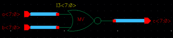
Schematic for eight bit OR
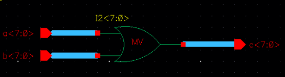
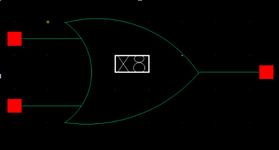
Symbol for eight bit OR
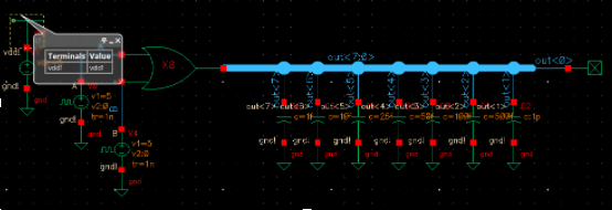
Test schematic for eight bit OR
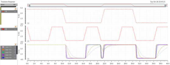
Simulation for eight bit OR are as expected. Output is only low when bot input bits are low.
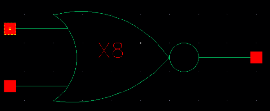
Schematic for eight bit NOR
Symbol for eight bit NOR
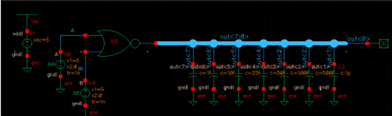
Test schematic for eight bit NOR
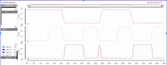
Simulation results were as expected. Output is only high when both inputs are low.
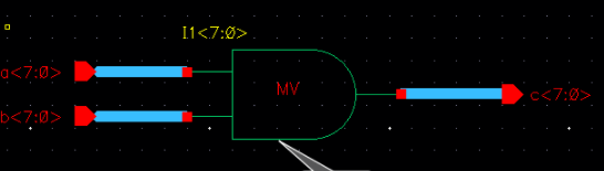
Once students were done designing and testing their eight input
gates, they were expected to move onto designing a 2:1 MUX. To start a
single MUX was to be designed and tested before using busses and arrays
to make an eight wide MUX.
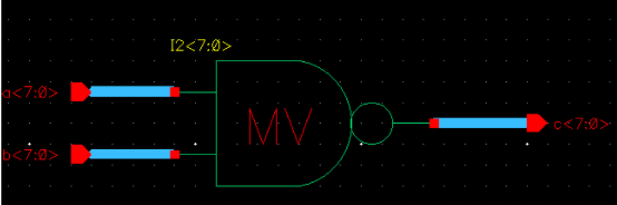
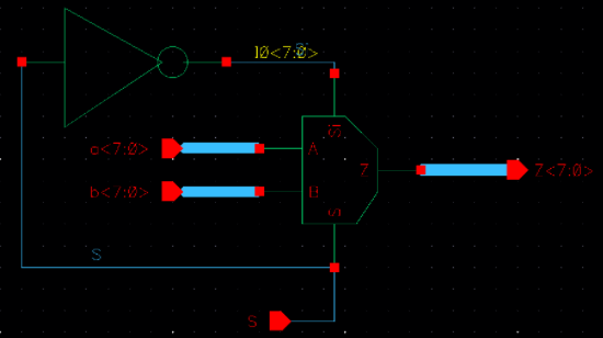
Below is the schematic of a 2:1MUX with four inputs and a single output.
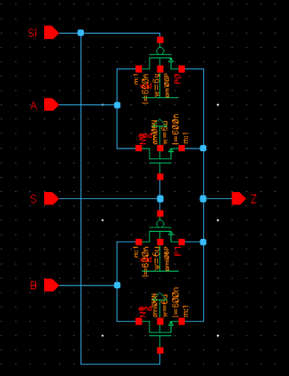
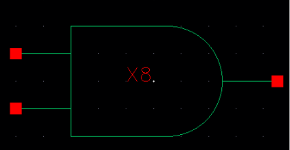
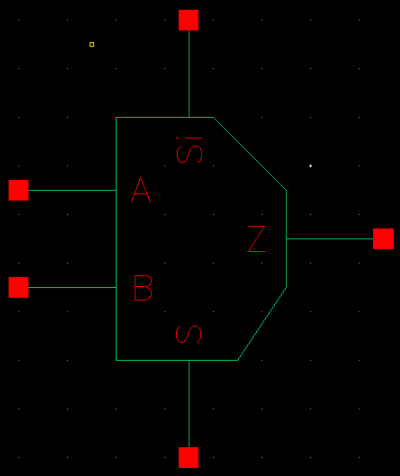
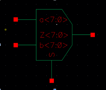
The symbol for the MUX is as shown below.
A test schematic for the 2:1MUX. This schematic includes the inverter designed in lab 5.
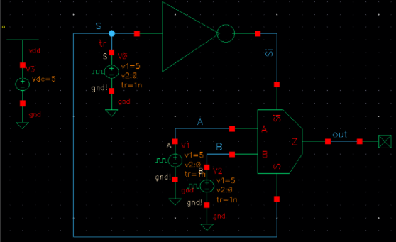
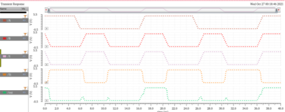
The simulation results are as shown below. The purpose of a MUX is
to allow a set amount of inputs through. This is done by using a select
bit to determine which input or inputs are passed through to the
output. For this example, students designed a 2:1MUX meaning that a
single input bit is used to determine which of the two inputs will pass
to the single output. Initially, the select bit is a "0" meaning that B
will pass through, which can be seen in the output results. B was low,
so therefor the output was also low. After every switch in the select
bit, the output was adjusted to match the input that was to be passed.
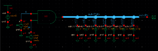
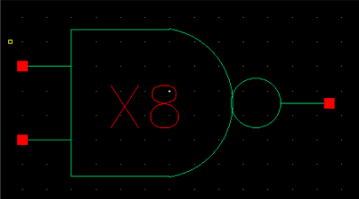
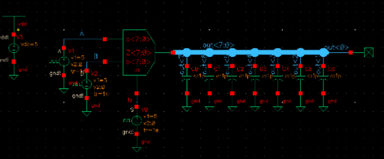
Now that the single mux was designed and tested, students were to
implement an eight wide 2:1MUX. For this schematic the Si input was
automatically set by the implementation of the inverter. This reduces
the amount of individual inputs this design will have. The nodes and
instance name were also adjusted to match the width of our MUX. For
eight MUX's students used <7:0>.
The symbol for this eight wide MUX is as shown below.
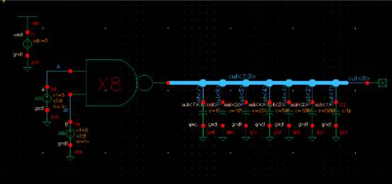
Test schematic for eight wide 2:1MUX.
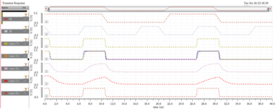
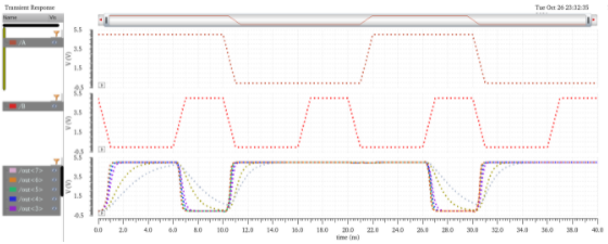
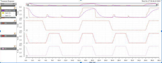
The results for this test schematic are as shwon below. Every
output is accounted for and match the intended function of the MUX.
That is, passing the input selected by the S input.
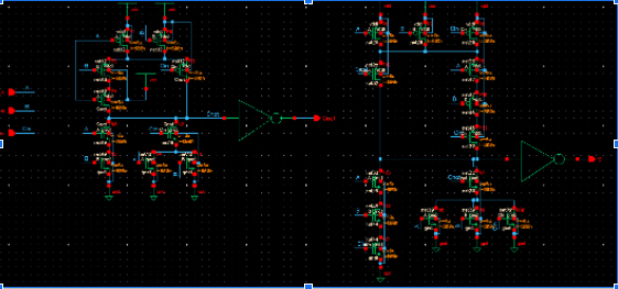
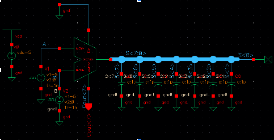
The final step of this lab was to design, test and layout an 8-bit full adder.
Students
recreated figure 12.20, which is as shown below. Due to the complexity
of the design, wires were ommitted. Instead, nodes were merely labeled
ot keep a clean interface. This schematic only represents a single full
adder. Once the design was completed, students implemented an 8-bit
wide full adder.
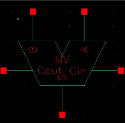
The symbol for the full adder is as shown below. This matches the symbol of the full adder designed in lab 6.
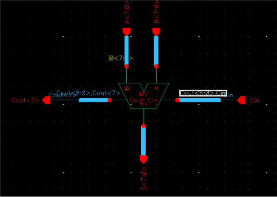
Once the single adder was completed, students worked towards an
8-bit adder.The notation is similar to those created previously, but
now there is signals being passed from one component to the next. To
account for this, the labeling of the wires is different. Ordereing
from most significant to least significant, the bits are labeled on the
connecting nodes. The inputs were labeled "Cout<6:0>, Cin"
showing that Cin<7> is attatched to Cout<6>. Cin<6>
is then attatched to Cout<5>. This pattern happens all the way
down to Cin<0>, which is then attatched to the original
Cin input.
The symbol for this 8-bit full adder is as shown below.
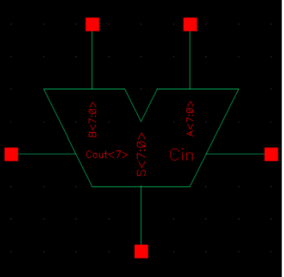
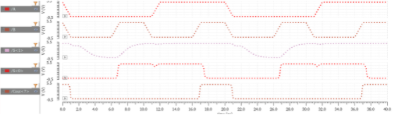
A test schematic was created to test the functionality of this symbol.
The results are as expected. If Cin is a "1" along with both
inputs, the Cin propagates. This can be shown at 17.0ns where Cout
rises.
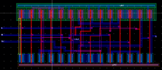
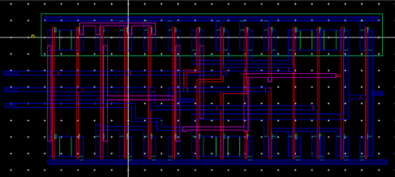
Now that the functionality of this adder has been tested, students were to layout this full adder.
The layout is as shown below.
Layout is DRC clean.
Extracted view of layout
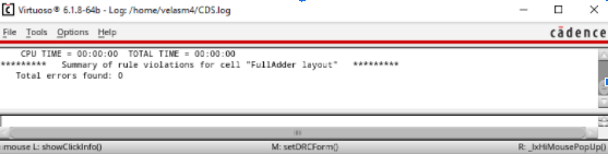
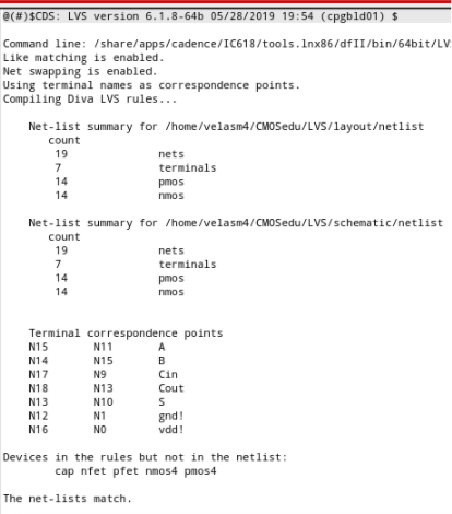
Layout was then to be LVS checked by comparing it to the full adder schematic.
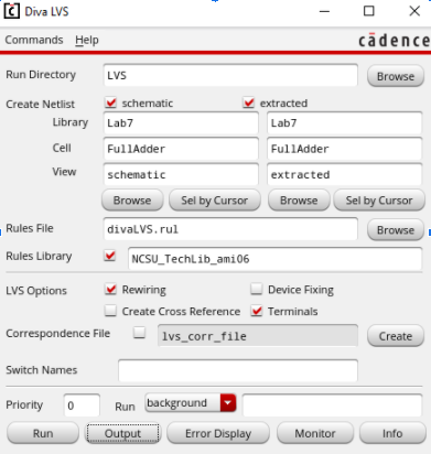
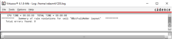
Layout is LVS clean.
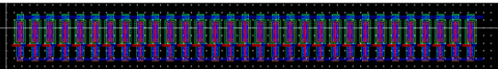
The layout was then instantiated eight times to recreated the 8-bit full adder.
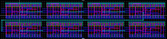
Layout is DRC clean.
This concludes Lab 7.
Lab7.zip
Return to Labs