Lab 6 - ECE 421L
Authored
by Michael Velasquez
velasm4@unlv.nevada.edu
October 6, 2021
Lab
description
Design, layout, and simulation of a CMOS NAND gate, XOR gate, and Full–Adder
Prelab Content
The
prelab had students design, layout and simulate a NAND gate which will
eventually be used in a Full Adder circuit in the lab.
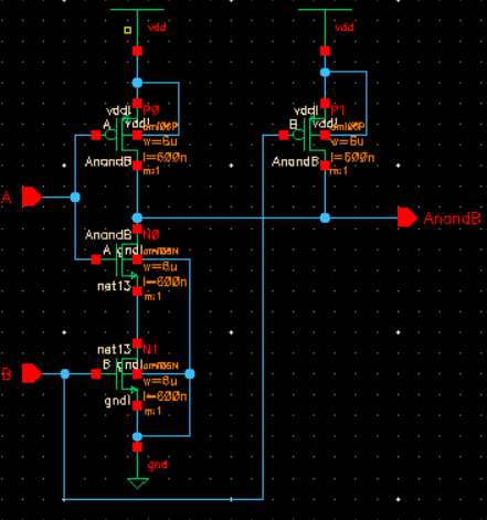
To
start off, the schematic was designed using both NMOS and PMOS
transistors with a size of 6u/0.6u. The inputs were labeled A and B,
while the output was labeled AnandB. This means that the output is
expected to be logic "1" in any case except A="1" AND B="1"
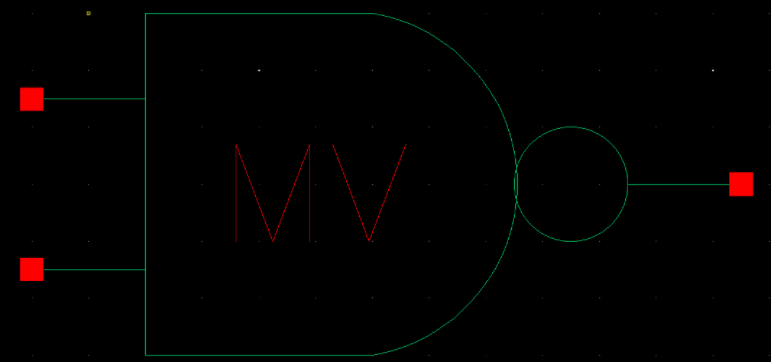
A symbol was then created resembling the NAND gates students were introduced to in CPE 100.
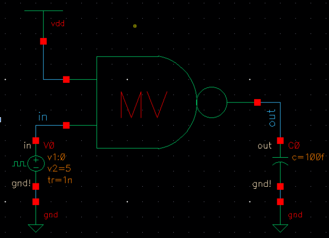
In
order to test the NAND gate's functionality, students designed a
circuit where the inputs were attatched to VDD and a pulse source. The
output was attatched to a load of 100F.
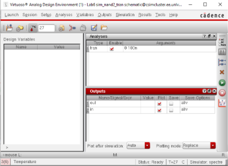
After launching the ADE,
students were to assign VDD as a global source with a value of 5V. This
replaces the need to connect a DC voltage supply to VDD in the
schematic. Any simulation of this schematic will assume VDD to be 5V.
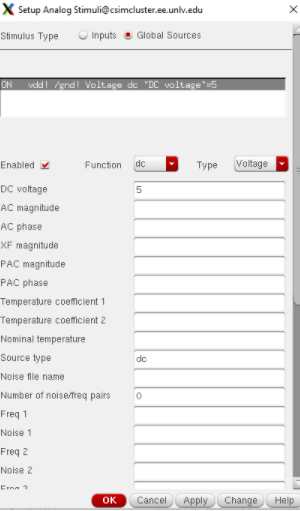
The settings for the simulation are shown below. A transient analysis
of 100ns was chosen to show three periods of the pulse source.
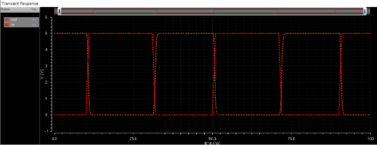
The simulation results are as shown below. When the pulse voltage
source is on, both inputs of the NAND gate are set to VDD. According to
NAND gate logic, this means Vout should be 0V. The results accurately
represent this prediction.
A layout was then made for the NAND gate.
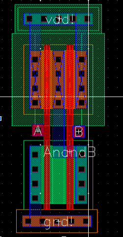
Layouts were expected to be DRC clean.
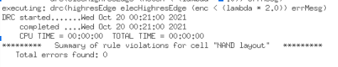
An extracted layout was created so that the LVS check can be ran.
To check LVS students were to compare the schematic and extracted layout of the NAND gate.

NAND gates were expected to be LVS clean.
This marks the end of the prelab content.
Lab Content
This lab focuses on the design, layout and simulation of a full adder.
A full adder is made using NAND and XOR gates. Students already
designed a NAND gate in the prelab, so the first step of the lab is to
design a XOR gate.
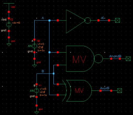
Below shows the schematic of the XOR. This gate is also made of 6u/0.6u NMOS and PMOS transistors.
The symbol created represents the gate symbol taught in CPE 100.
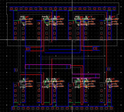
The layout of the XOR gate is as shown below. This is the first layout
that students have used the metal2 layer. To connect to the metal1
layer, students were able to use the m1_m2 via. There are also
instances where m1_m2 and m1_poly vias were stacked to connect across
multiple layers.
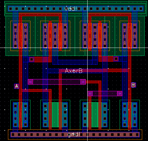
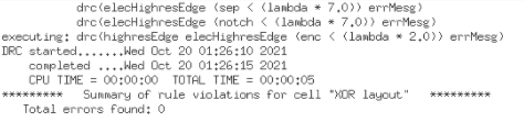
The XOR layout was expected to DRC clean.
An extracted layout was created so that students can LVS their design.
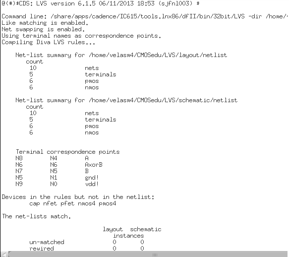
The LVS was to compare the schematic and extracted layout of the XOR gate.
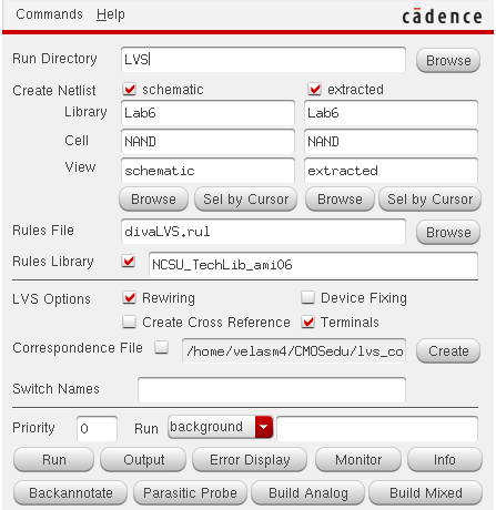
A clean LVS result for the XOR gate is shown below.
A test schematic was made to ensure all required gates are operating as
intended. This single simulation will prove that the students' NOT,
NAND and XOR are functional. The pulses operate and two different
frequencies to test multiple input cases.
The simulation settings are as shown below.
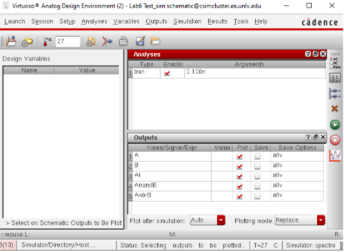
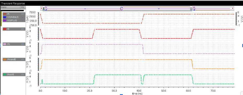
The input and output waveforms are shown below. Initially, both input
waveforms are logic "0" so the NAND and inverter are expected to be
logic "1" while XOR is expected to be logic "0". This matches the
simulation results. Once B shifts to logic "1" the only expected change
on the output is for XOR to shift, which which is shown at time
t=22.5ns. The rest of the waveforms follow the intended results.
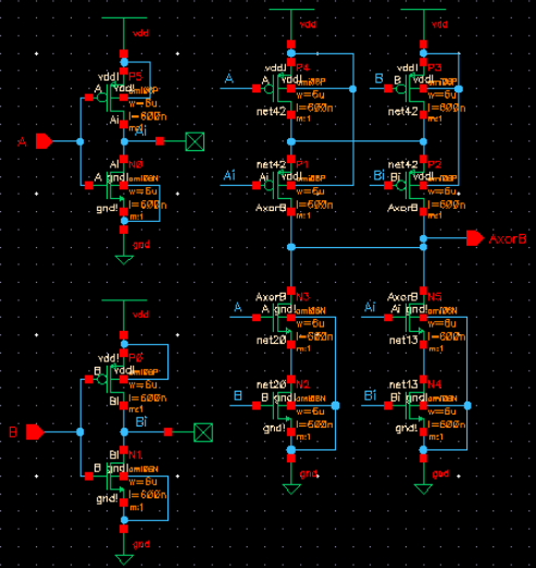
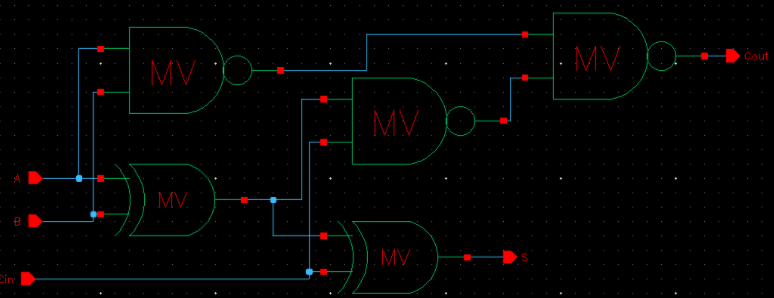
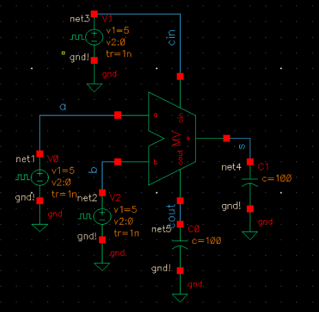
Now
that the gates have been proven to work, the full adder can be
constructed. The schematic is as shown below. Three inputs (A,B and
Cin) and two outpus (Cout and S) will lead to a circuit that is able to
do bit addition.
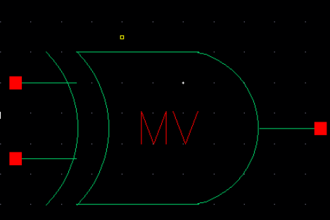
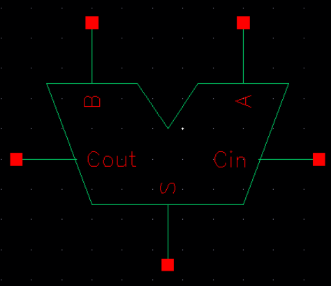
The symbol for the full adder follows what was taught in CPE 100.
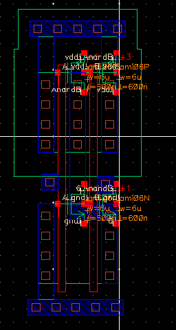
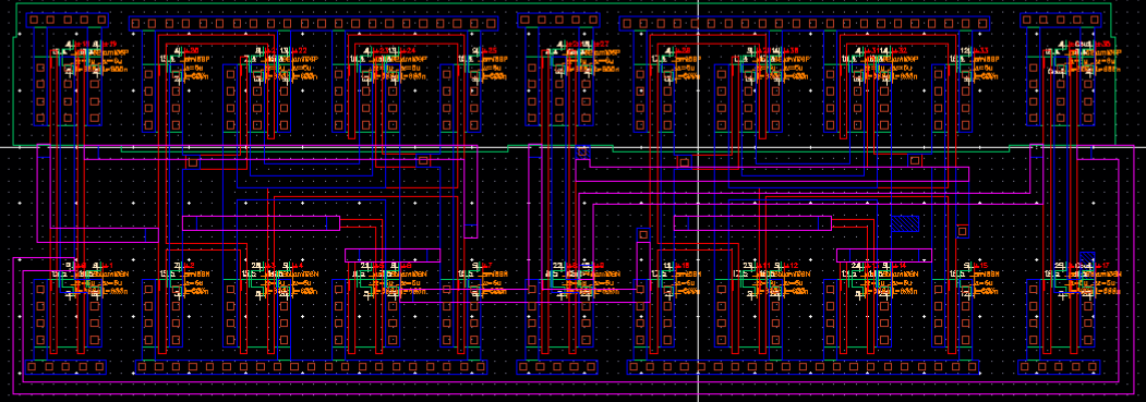
The layout of the full adder is shown below. The NAND gate was adjusted
to match the width of the XOR gate. This allows for VDD and GND to be
in line for every gate. Space is created inbetween the PMOS and NMOS
transistors is created so that connections can be made with ease.
Metal1, metal2 and poly layers were used to create said connections.
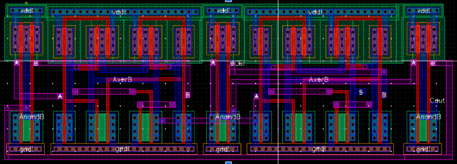
As always, the layout was expected to be DRC clean.
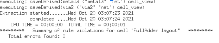
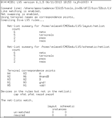
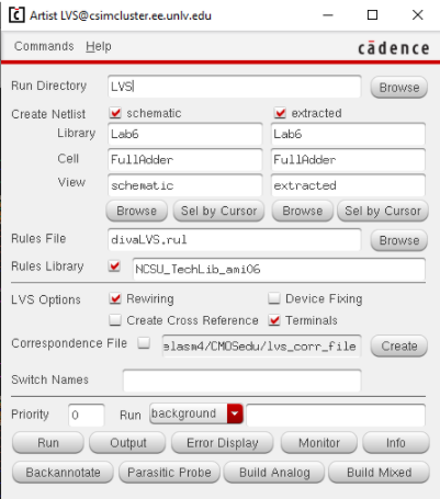
An extracted layout was created so that an LVS check can be ran.
The LVS check for the full adder was to be ran between the schematic and extracted layout.
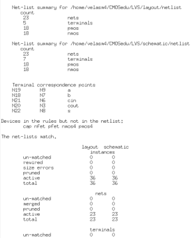
LVS output shows that the netlists match.
After completing the full adder, students were to test the
functionality of the circuit. A test schematic was made with the inputs
(A, B and Cin) were attatched to pulses with varying frequencies to
test functionality in various cases.
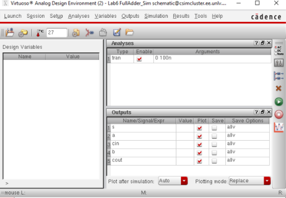
The ADE and settings of the simulation are as shown below.
As
expected, the results of the full adder show bit addition with various
sequences. Initially A, B and Cin all equal "01". "01" + "01" + "01" =
"11" according to binary addition. This is represented by Cout and S
both equalling VDD. Once all three inputs shift to logic "0" the output
represents "00" + "00" + "00" by dropping S and Cout to logic "0". The
following waveforms represent binary addition accurately.
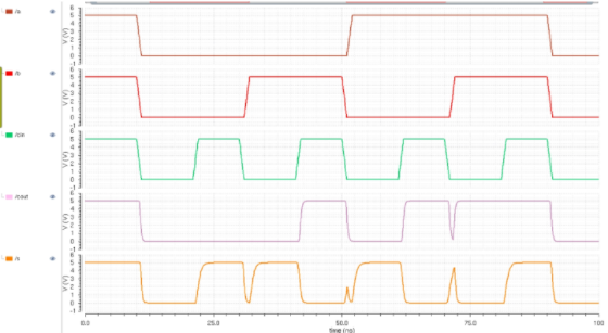
One
thing to be noted about the simulations is that there appears to be
glitches in the outputs after a transition of inputs occur. These
glitches show through peaks and troughs in the output waveforms. This
can be explained as logic signals cannot instantaneously switch in real
life circuits. This phenomenom is represented by a 1ns rise and fall
time. Within this second, all values between logic "1" and "0" are
seen. Within this time it is uncertain whether the MOSFET devices are
on and off, and the samples taken within the time will be ambiguos. In
CPE 100 it was taught that this time results in a lot of uncertainity
as the outputs will bounce and no samples can be taken.
This concludes Lab 6.
Lab6.7z
Return to Labs