Lab 8 - ECE 421L
Authored
by Charlene Drake, Luis Garcia-Rivas, Michael Velasquez
Emails:
drakec2@unlv.nevada.edu
garciari@unlv.nevada.edu
velasm4@unlv.nevada.edu
December 1st, 2021
Lab
description:
Lab 8- Generating a test chip layout for fabrication as a group of three.
Prelab Content:
For
the prelab, we were tasked with completing Tutorial 6 on Dr. Baker's
website. Tutorial 6 covered the topic of pad and pad frames. These pads
are what give all of the circuits we've designed up until now
functionality. Bonding pads is where connections are made in real life
devices, rather than just having wires connected in an online setting.
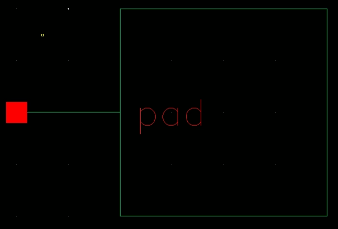
To start off, a schematic was made of any given pad. This was done by simply placing an InOut pin labeled pad.

A schematic was then created in order to represent the pad that will be used for our schematic.
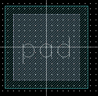
Similar to any other lab, a layout was created out of our schematic.
The metal3 layer is mainly used to ensure that the connections can be
made cleanly.
Busses and arrays were then used to keep a clean and organized
schematic for a padframe. The padframe we created includes 40 pads
which allows for the required connections for the lab to come.
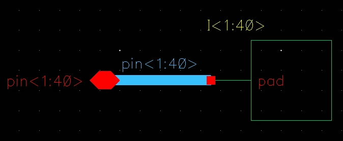
The symbol for this padframe schematic is as shown below. Pin<1:40> represents the 40 pads present in the schematic.
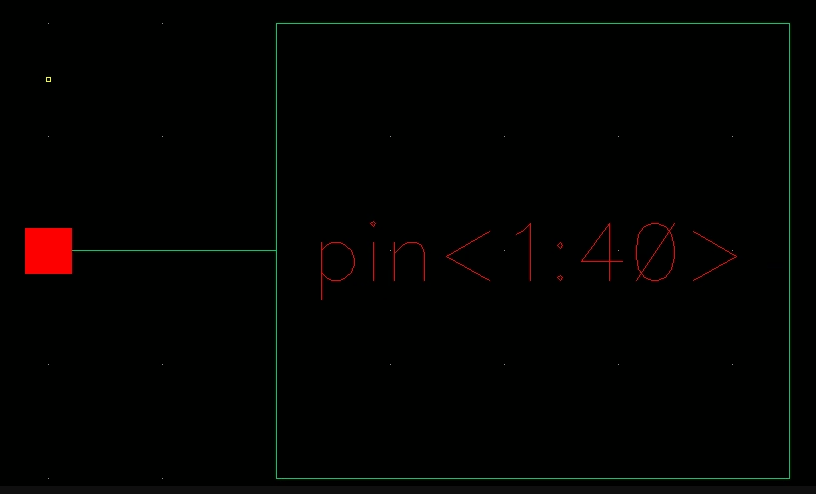
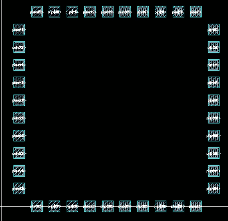
A layout of the padrame was created. The square organization of the
padframe will help keep an organized and spacious area for the
components to be placed into.
Lab Content:
Now
that the layout of the padfram has been created, components are
required to create a functional chip. With 40 pads we have plenty of
space for multiple functions. Up until this point in the lab, students
have created many circuits which will be used in our designed chip.
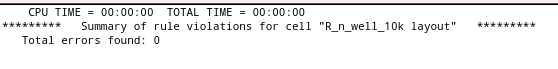
To start the chip, we implement a 25k n-well resistor. This is created using the n-well and res-id layers.

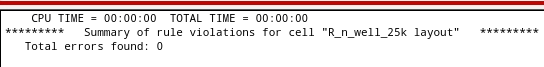
Layout of the 25k resistor is DRC clean.
To
check the resistance of our component, the layout view was extracted.
Of course it is unlikely to get the exact intended value, so there is a
tolerance for the value.
The 25k resistor was created with the intent of creating a voltage
divider. The second resistor used for this voltage divider is a 10k
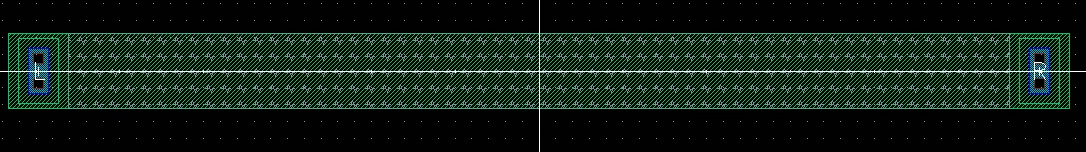
resistor. Below is the layout of the resistor.
Resistor DRC is clean.
Again, the resistor is extracted to check the value, which is slightly off of the intended design.
 .
.
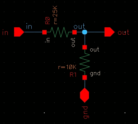
A
schematic of the voltage divider was then created. The pins shown in
every following schematic is what will connect to the pads laid out in
the prelab.
A symbol was then created to represent the voltage divider. For every
following component the symbols will resemble what is taught in
circuits and CPE classes.
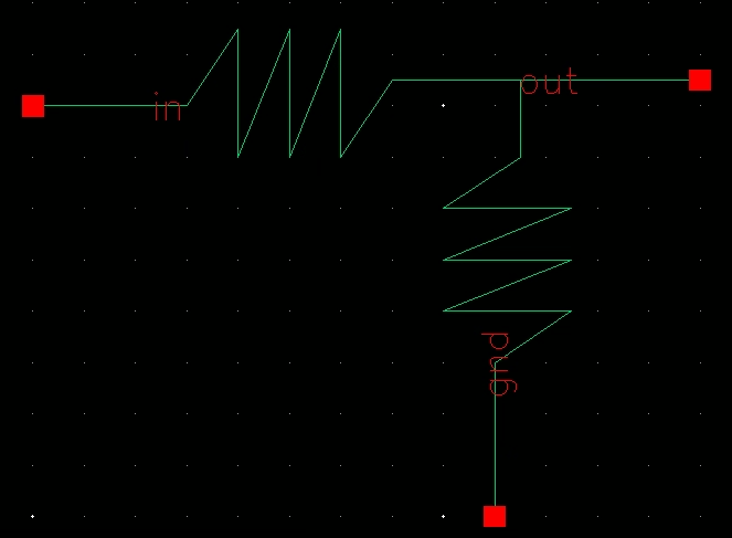
The layout of the voltage divider is a combination of the previous two
layouts. The difference in length shows the difference in values.
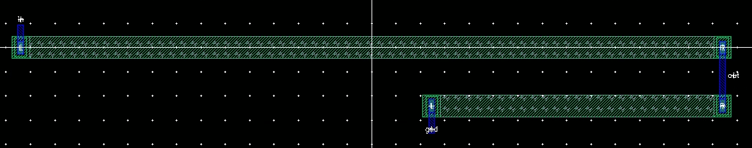
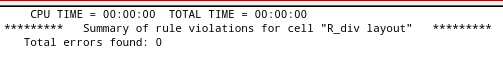
R_div voltage divider DRC is clean.
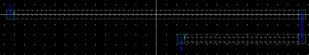
Extracted view of R_div is as shown below.
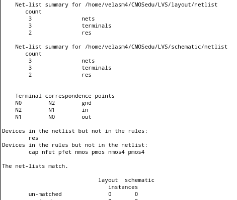
LVS check was ran to ensure the layout matches the schematic.
The main difference between the following components, and the
components created in previous labs is that a global GND and VDD are
not used at every level of each design. Pins that are of InOut are used
to create the connections of VDD and GND throughout the layers. This is
because the path from the pad to each transistor in every design must
be specifically designated in actual chip design.
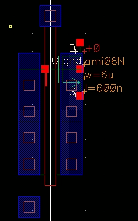
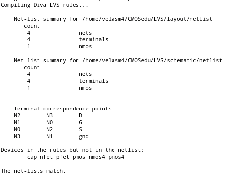
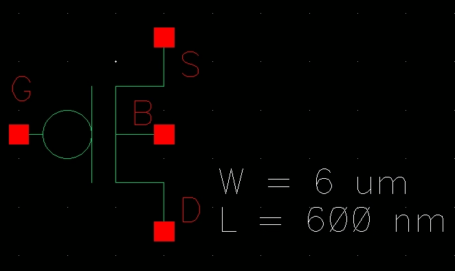
The next components to be placed on the chip are 6u/0.6u NMOS and PMOS devices.
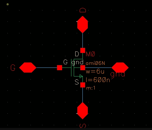
Schematic of NMOS:
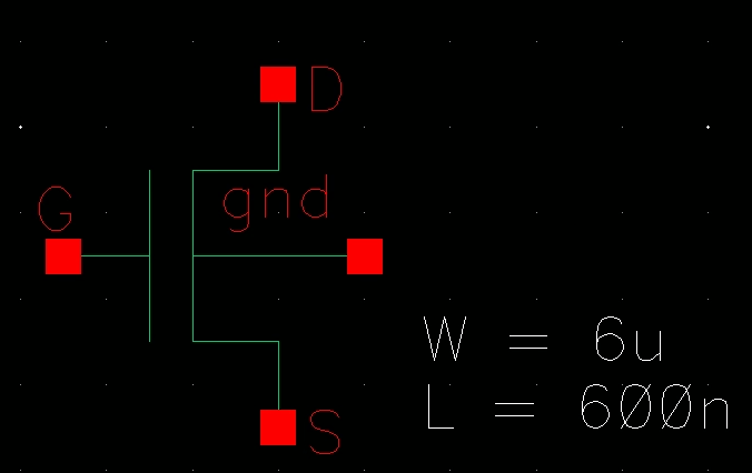
Symbol of NMOS:
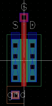
Layout of NMOS:
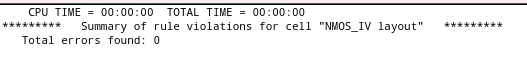
DRC results of NMOS:
Extracted view of NMOS:
LVS Results of NMOS:
Schematic of PMOS:
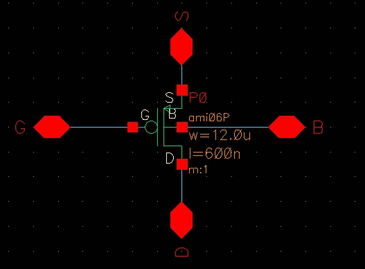
Symbol of PMOS:
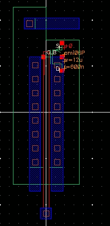
Layout of PMOS:
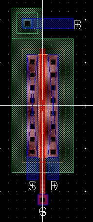
DRC Results of PMOS:
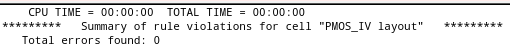
Extracted View of PMOS:
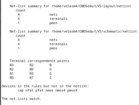
LVS Results of PMOS:
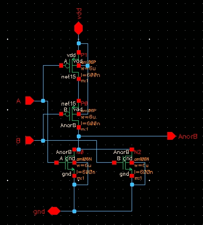
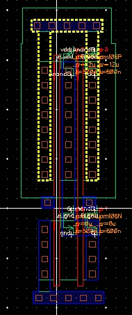
Logic Gates were also implemented onto the chip. Specifically, a
two-input NAND and NOR was placed onto the chip. These gates were
designed using 6u/06u CMOS devices.
NAND Schematic:
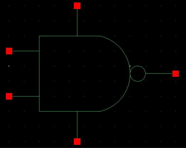
NAND Symbol:
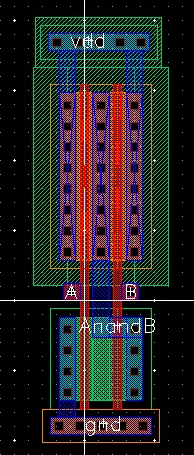
NAND Layout:
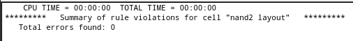
NAND DRC Results:
NAND Extracted View:
NAND LVS Results:
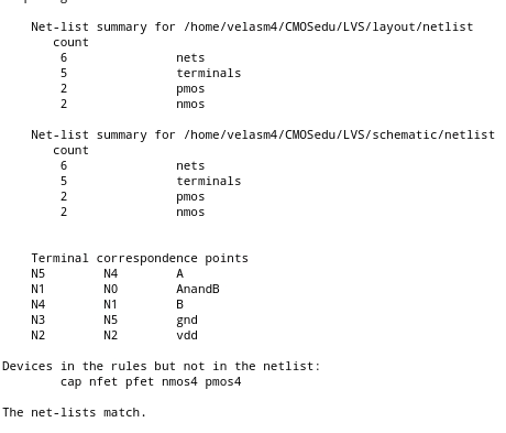
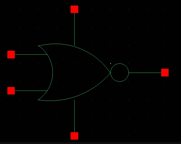
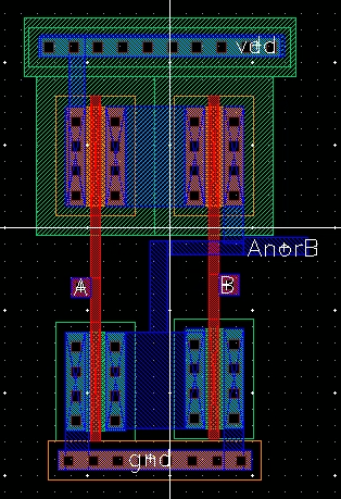
NOR Schematic:
NOR Symbol:
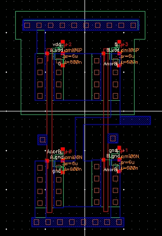
NOR Layout:
NOR DRC Results:
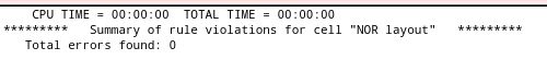
NOR Extracted View:
NOR LVS Results:
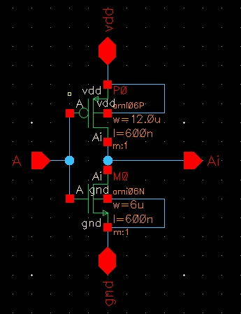
Inverter Schematic:
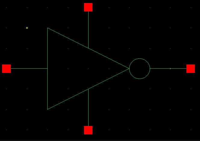
Inverter Symbol:
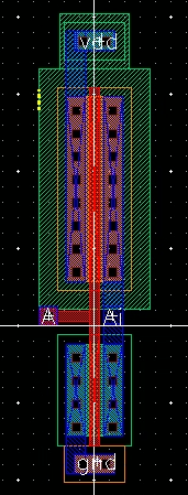
Inverter Layout:
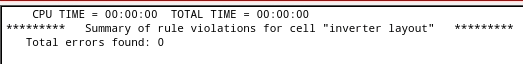
Inverter DRC Results:
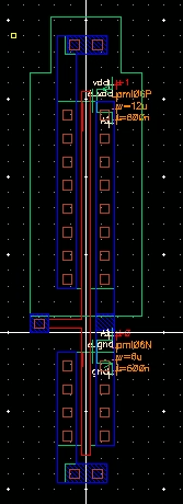
Inverter Extracted View:
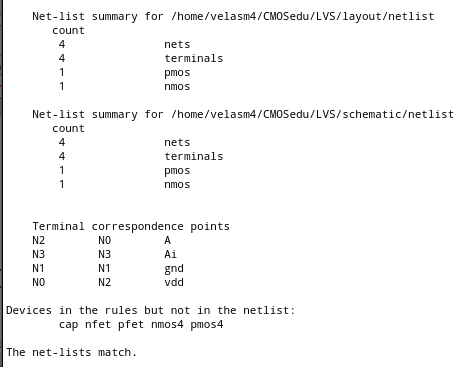
Inverter LVS Results:
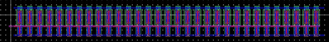
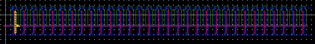
Using the inverter shown above, a 31 stage ring oscillator was created.
Ring Oscillator Schematic
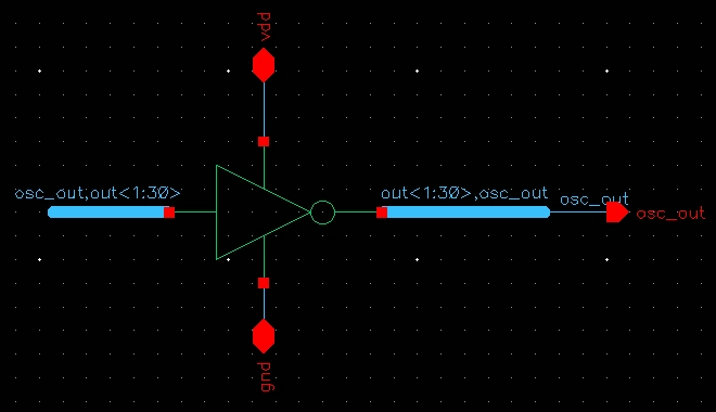
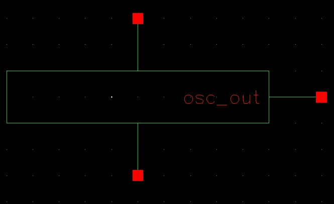
Ring Oscillator Symbol:
Ring Oscillator Layout:
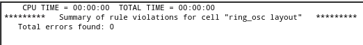
Ring Oscillator DRC Results:
Ring Oscillator Extracted View:
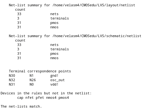
Ring Oscillator LVS Results:
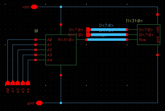
Finally, a course project was to be placed onto the chip. For the lab,
a Register File was created that was to store 32 8-bit words based on
five adress bits and eight bit lines. Unfortunately, there were two
reasons we had to omit this layout from the final chip layout. First,
the register file created was too large to fit of the padframe that was
created in the layout. For previous semesters these chips were actually
fabricated, so the size specifications were important. The layout of
the course project was too large to fit within these dimensions. The
next reason was the amount of pins this specific design would take up.
If there was an inverter placed inside the 8-bit array, the RF would
take 13 pad but this is not the case. After all of the other components
there is not enough space to compensate for 30 unique pins. For these
two reasons we have omitted the RF from the chip design but the process
will still be explained as if we were able to fit this component.
Register File Schematic:
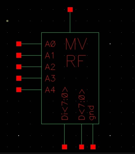
Register File Symbol:
Register File Layout and Extracted View:
Register File DRC check:
Register File LVS Results:
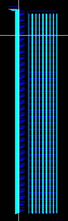
Once all of the components were created, a schematic was created to
show the pin connenctions in a clean way. All components described
above were places except for the RF. If we were able to fit a register
file in, the adress bits would take pin<26:30>, D inputs would
take pin<31:38> and VDD would be pin<39>.
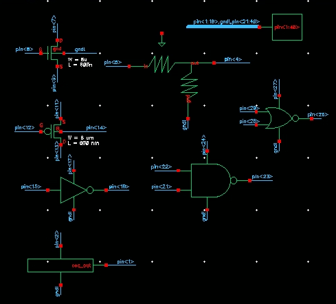
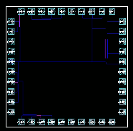
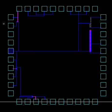
The padframe with all components connected is shown below. All
connections were made on metal1 and metal2, so they can be hardly be
seen. The common ground was made to be pin<20> which is connected
to all components. Each circuit has a unique VDD. This is to protect
the chip from a overall malfunction if there is ever to be a VDD to GND
short. Having unique VDD pads keeps every other component functioning
even if one fails.
Although every layout shown is relatively small, the register file would have taken a majority of the space if included.
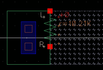
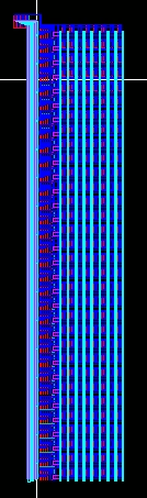
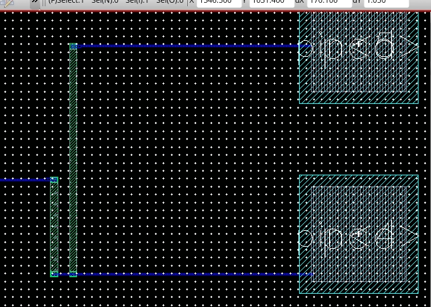
To show how connetions were made, blown up images of two of the components are shown below.
Ring Oscillator Connection:
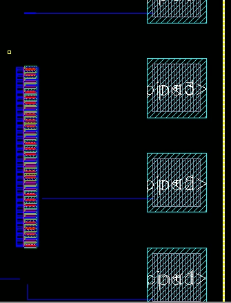
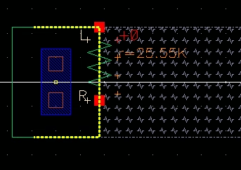
Voltage Divider Connection:
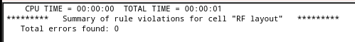
Layout of chip design is DRC clean.
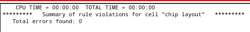
Below is the extracted view of the chip.
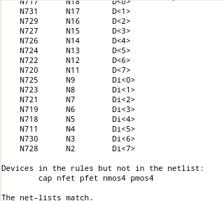
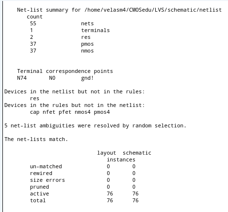
LVS results are clean, which shows that the layout of the chip matches
the schematic. With this, if fabricated, all components would be
functional if wired correctly.
Testing the chip created would be similar to testing any PCB or
Breadboard design. The bonding pads are where any connections can be
made. This is where you can solder a connection via jumper cables or
any other means of carrying a current. Pad 20 would need to be soldered
to any form of ground as a reference point. Other pads marked as VDD
must be connected to a voltage source. This can be anything from a
battery, to the power supplies located in the lab. Using an
oscilloscope or multimeter, you could test for any measurments you may
want. Using bonding pads five and four you can test resistance. This
can be done by setting the multimeter to resistance and touching each
probe to the respective terminal. To test the oscillator, you would
connect the oscilliscope probes to ground (pad 20) and pad 1.
This concludes Lab 8.
Lab8.zip
Charlene Drake Labs
Luis Garcia-Rivas Labs
Michael Velasquez Labs