Lab Project - EE 421L
Authored
by Ricardo Rodriguez
UNLV E-mail: rodrir15@unlv.nevada.edu
November 24, 2021
Project:
The
goal of the project was to make an 8 bit 32 word register file. The
register file has words going from 31 to 0. My project has a total of22
different data related pins. There is an 8 bit bus for the input and a
separate 8 bit bus for the Data values. Since we have 32 words, there
are 5 bits for the addressing. There is a
single pin for the Read/Write. In this design, R/W allows us to write
to our word when it is low and to read when it is a logic high.
The
process of making the register file started with the single bit Static
Random Access Memory cell. From there we can increase it an 8 bit word
and then create an array of words. This would connect to our row
decoder, which has an input of 5 bits and a total of 32 outputs, each
corresponding to a different word line. For example, 01011 would give
row 11 as a logic high and all other rows a logic 0. From there, we can
implement the R/W function by the use of some NMOS devices and an
inverter to allow us to switch between the read and write function.
Schematic Work:
Single SRAM Bit Cell Schematic:

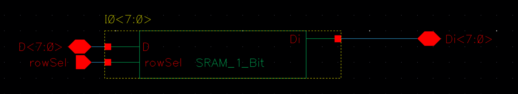
Single SRAM Bit Cell Symbol

Layout:
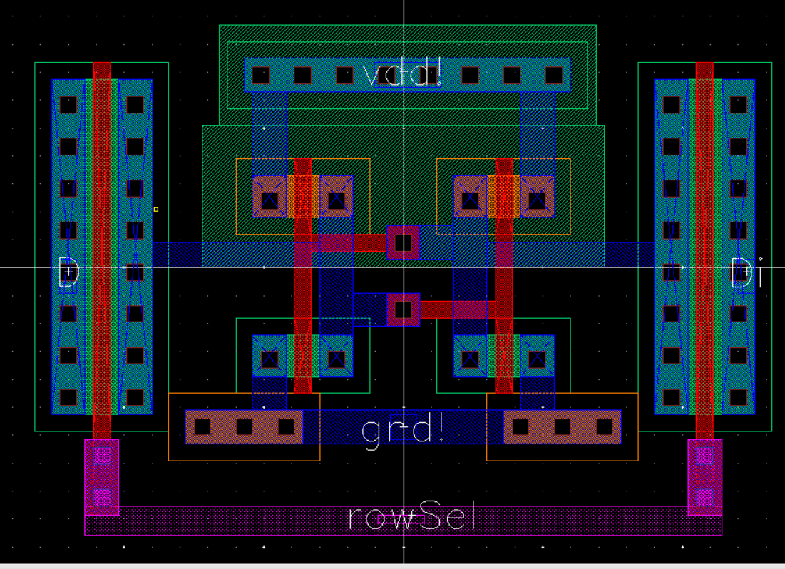
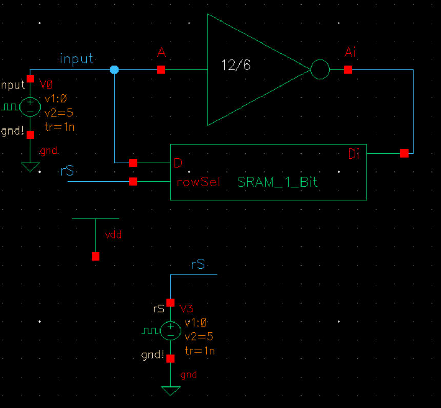
Single
SRAM Bit Cell Simulation Schematic:
Single SRAM Bit Cell Simulation:
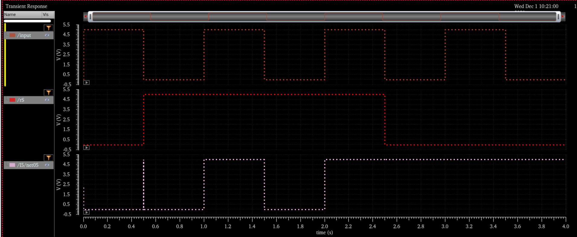
This
simulation lets us write to our cell as our RS (row select) functions
as our data for the word line. We see that whenever that RS is low, our
stored data (bottom graph) does not change but as soon as RS is high,
our stored bit mirrors the input until RS goes low again.
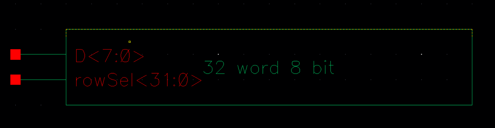
8-bit
SRAM Cell Schematic:
8-bit SRAM Cell Symbol

Layout:

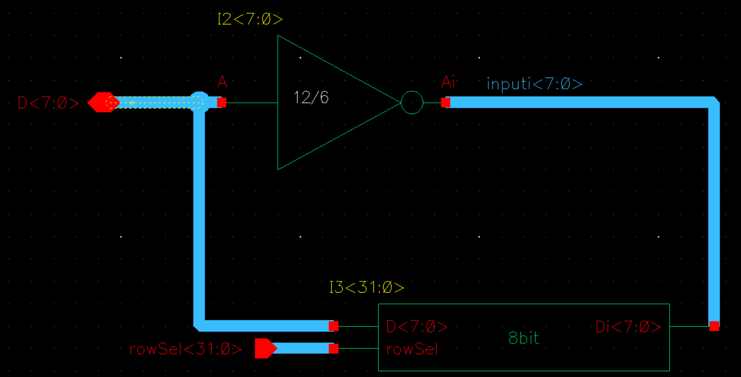
8-bit
SRAM Cell Simulation Schematic:
8-bit SRAM Cell Simulation:
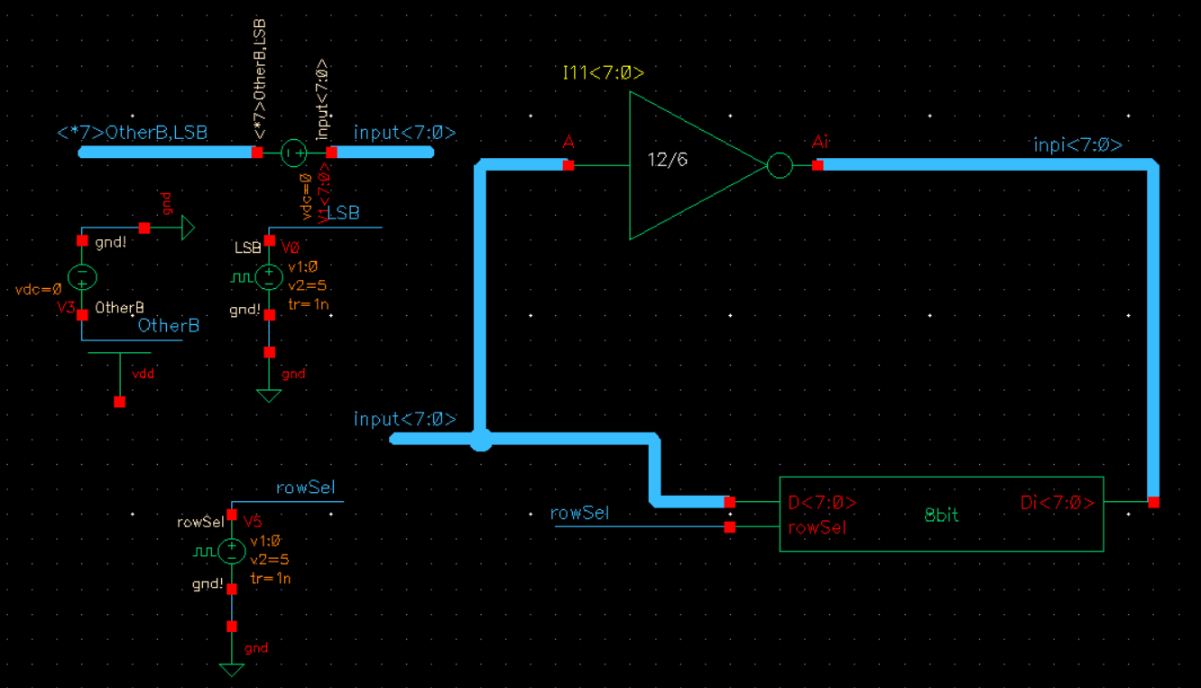
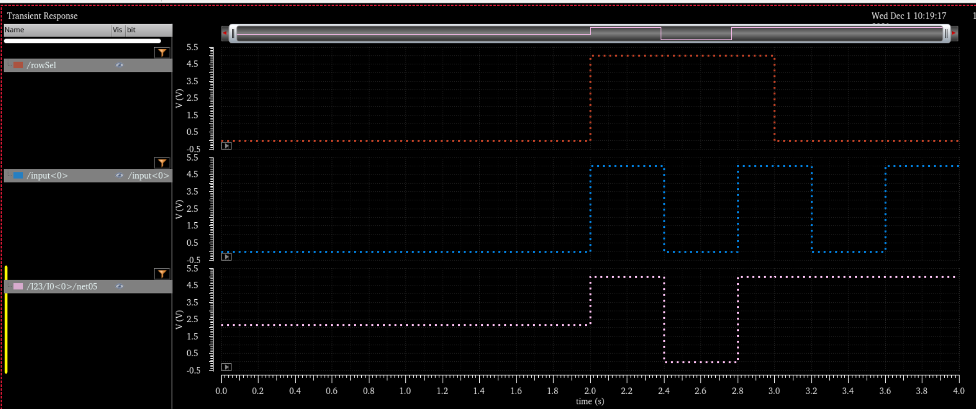
From
the sim schematic, we can see that the input will be varying
bit<0> or the least significant bit. All others will remain at
logic 0. Only when our word line input rowSel is at a high, our data in
our cell will be written to, otherwise the data will be stored. It is
also important to note that no initial conditions were used in the
simulation for our stored data resulting in a 2.5V initial voltage to
our cell.
32
Word Cell Schematic:
32 Word Cell Symbol
Layout:
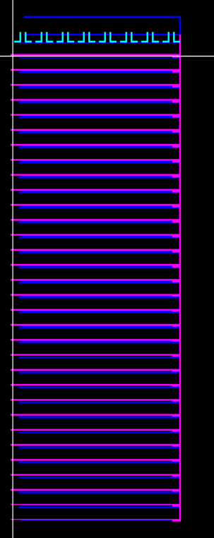

Layout Closeup:

The
layout of the array connects all 32 words together by their respective
bit. For example input<7> is shorted between all 32 words. Each
word has it's unique word line that will be connected to the output of
the row decoder. In this manner, we can write to individual words,
using the same data in.
Array Sim Schematic:
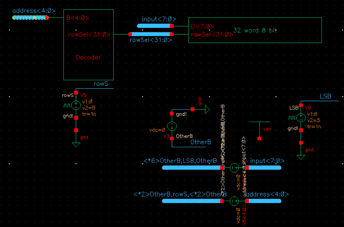
For
easier simulation, I connected the functioning row decoder (not yet
shown) to the array. This way, different words can be seen during
simulation and see how the array functions under changes in the
addressing.
Array Sim:
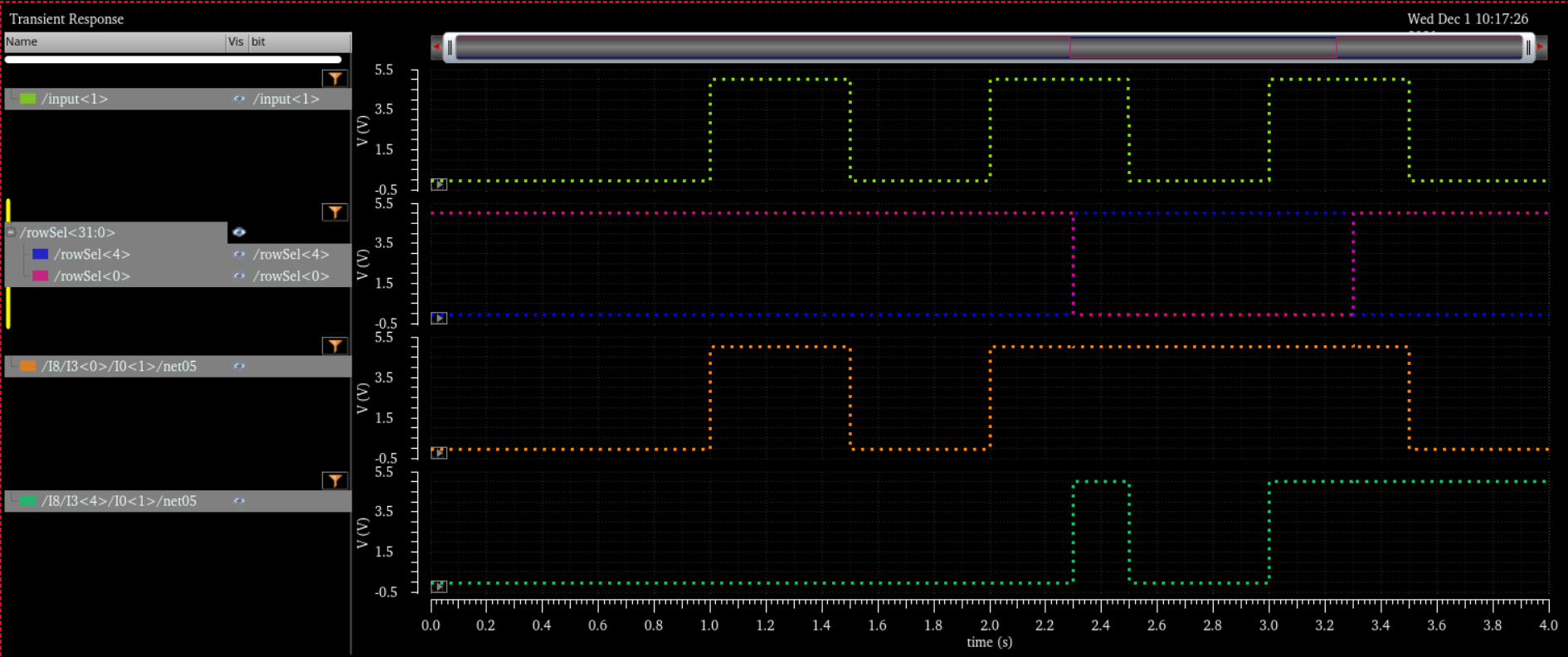
In
the simulation, we can see that our data on bit 1 is what is being
written and read from. At all points in time of the simulation,
the
array always has a word to write to.
For the intial addressing, we write to 00000 (0) which later changes to 00100(4).
At
around 2.3 seconds, we can see our address change occur and that our
bit 1 in address 00100 (green graph) is finally written to and follows along the
input while
our address 00000 (orange graph) remains constant until we change the address back.
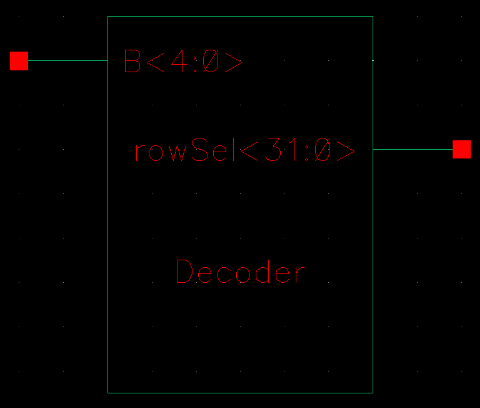
Row
Decoder Schematic:
Row Decoder Symbol

Layout:
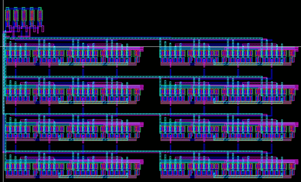
Row
Decoder Simulation Schematic:
Row
Decoder Simulation:


Just to see the function of the row decoder, our selected output/row will be alternating between Row0 and
Row1.
When all bits of the input is 0, we will get Row0, and when the
LSB is
logic 1, we get Row1.
To know which output will go high, we can look at the binary input of the address and convert it to decimal.
For example, 10010 will give a logic high to Row18 while all others remain at logic low.
Final Register File:
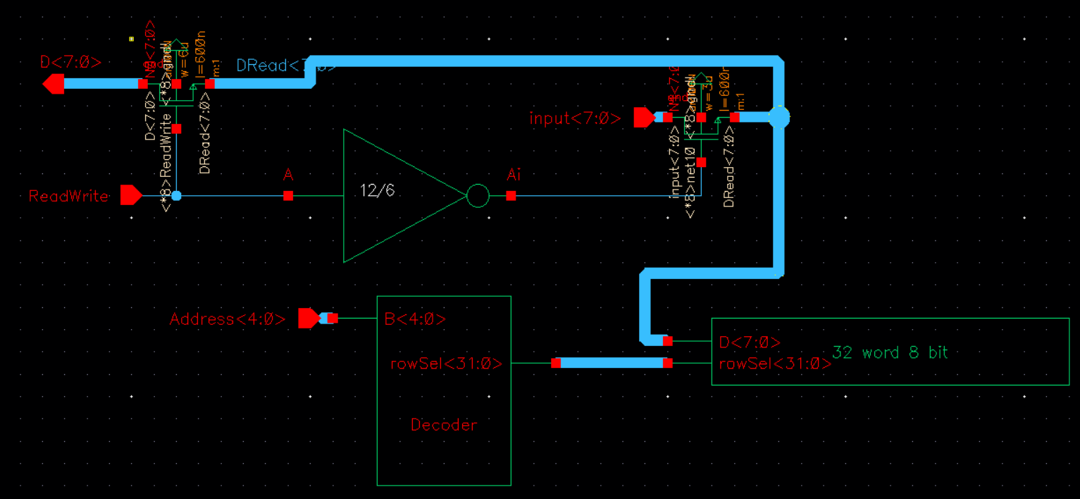
The
register file connected the decoder to the word lines of the array.
Since D<7:0> is an inputOutput pin, we can choose to read or
write to D. To implement the R/W function, we connect the signal and
it's compliment to the gates of two different NMOS transistors. The
drains of the devices will be shorted and connect to D of the array.
However, one transistor will have it's source at an Output D and the
other will have it's source to the input. Since we want R/W to write
when low, we connect the compliment to the input transistor and R/W to
the Output D transistor.
Symbol:

Simulation Schematic:

Simulation:
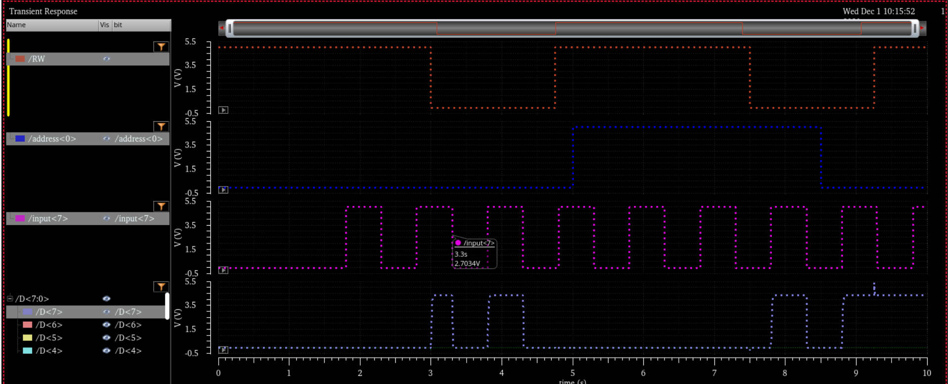
For
our simulation, we start by reading the values stored in 00000 or word
0. We can see that the RF output remains constant until R/W goes low,
which tells us that we can write to the address. When we change our
address, we can see that the R/W function doesn't change and allows us
to read the data that was in word 1 (00001).
It is until R/W goes low again where we can start wiriting to word 1.
Zipped directory of the project can be found here.
Return to my labs
Return to student labs

