8-Bit 32-Word SRAM - ECE 421L
Created and edited by Michael Parker
Email : parkem3@unlv.nevada.edu
Last updated : November 23, 2021
The
objective of this project was to design a register file (RF) that uses
an 8-bit word and has 32 words. The RF uses a 5-bit address to access
the
32
8-bit words. Other inputs to to the RF are 8 IO lines for reading and
writing, a control signal for indicating either a read or write to the
RF, and
VDD/ground.
Inverter
My
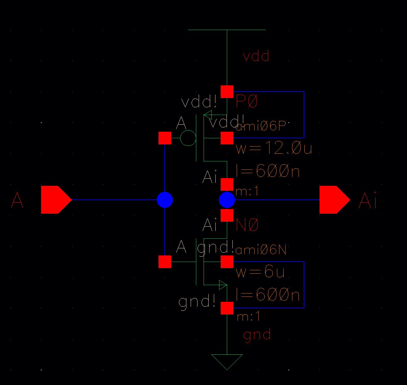
first objective for this project was to create an inverter for use
throughout my design. The schematic below creates a 12u/6u inverter
from which
the symbol below was created.

A
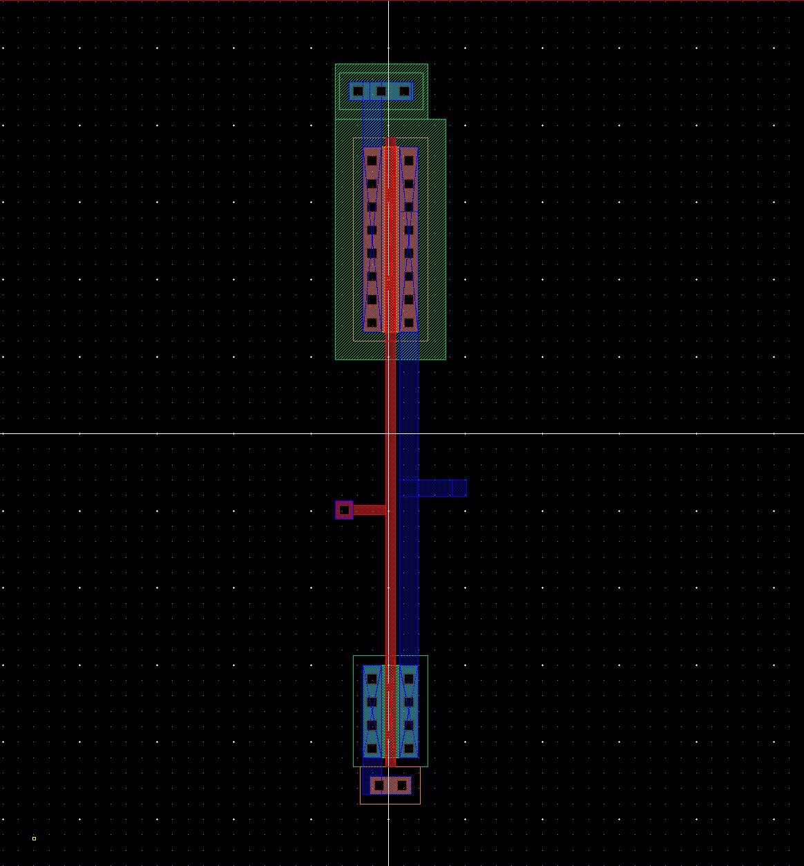
layout of the inverter will be needed later for instantiation. This
layout was the beginning of creating a standard cell. The creation of
this cell will
allow better allignment later in the design. Upon
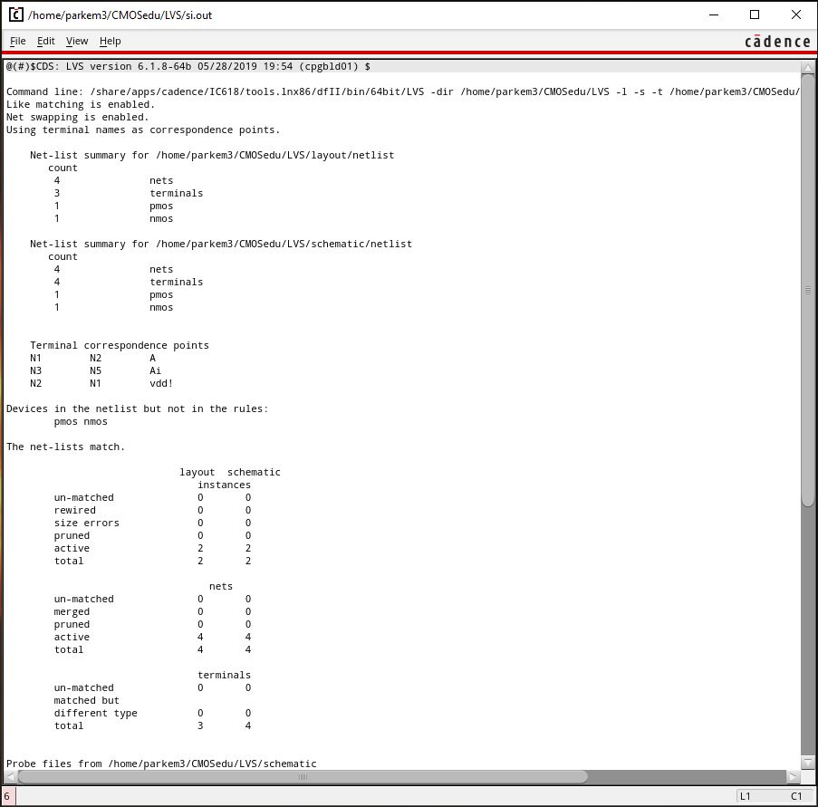
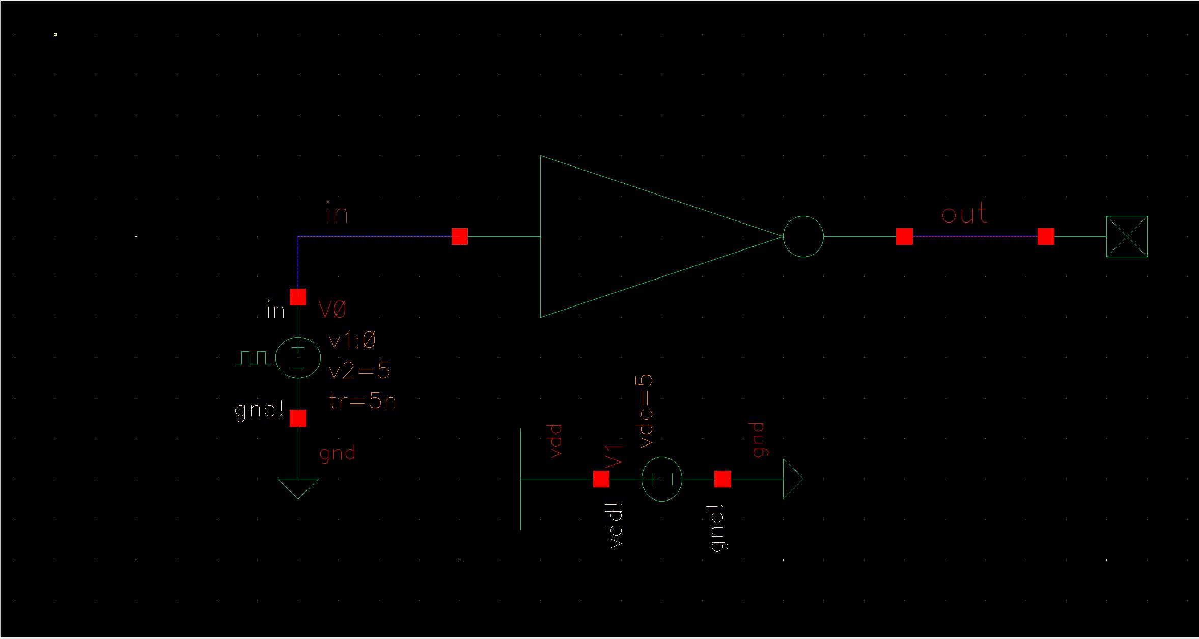
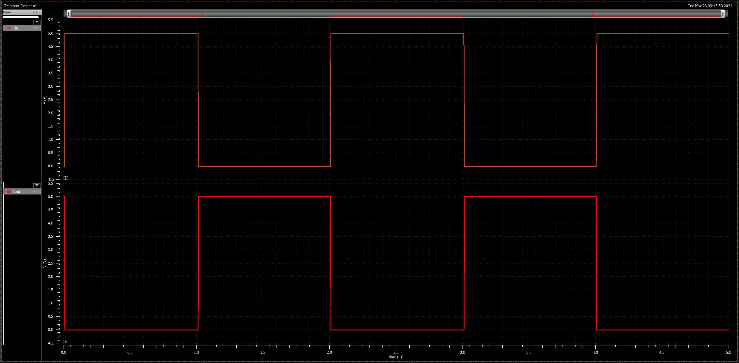
finishing the layout, a DRC, LVS and simulation were run to ensure
propper opperation.

Bit Cell
Once
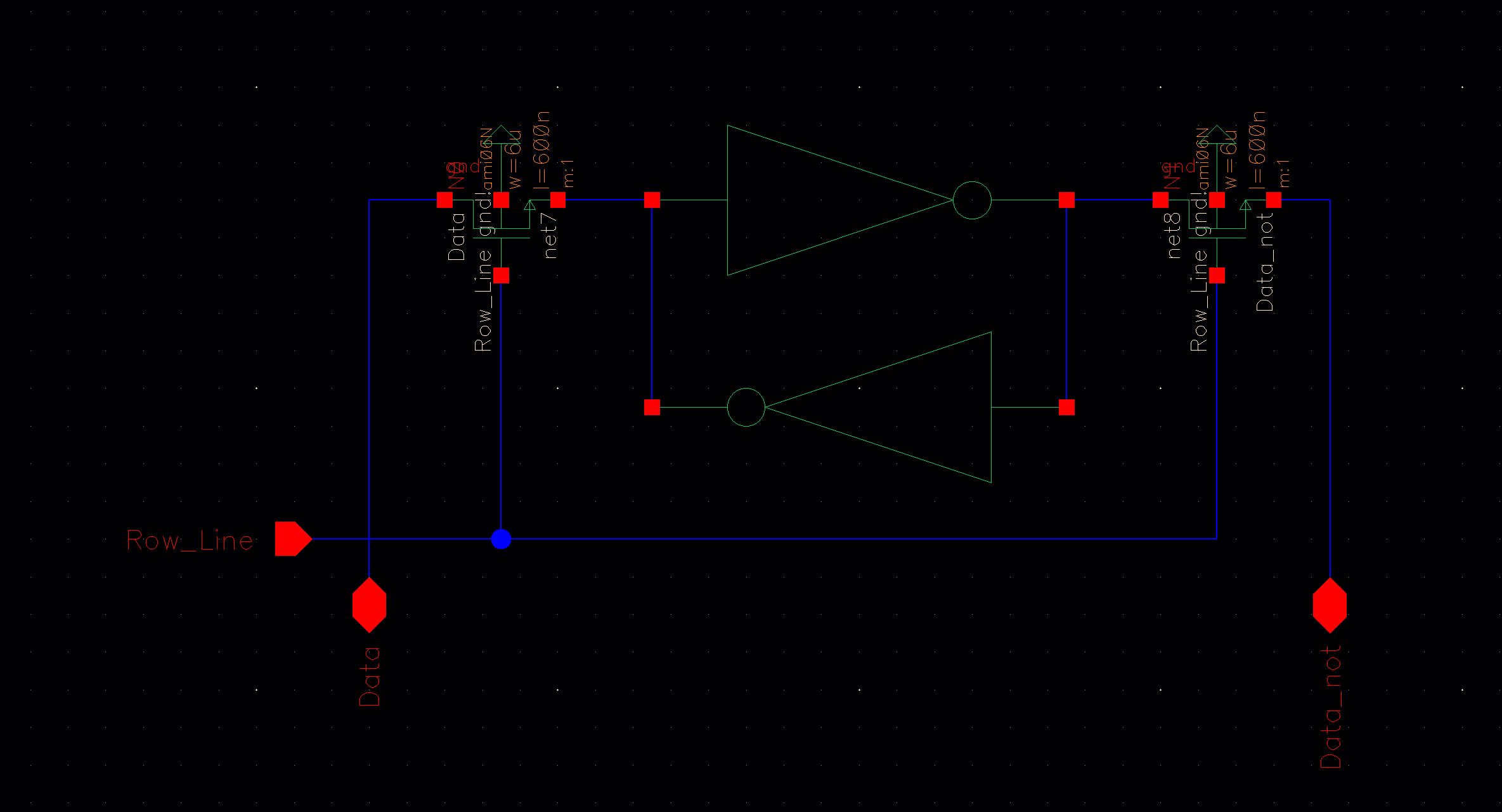
the inverter was completed, it could be instantiated twice in the
bit cell. The bit cell uses the Row_Line input to turn on the NMOS at
the
beginning and end of the circuit. This allows for reading and writing to the bit cell.
After
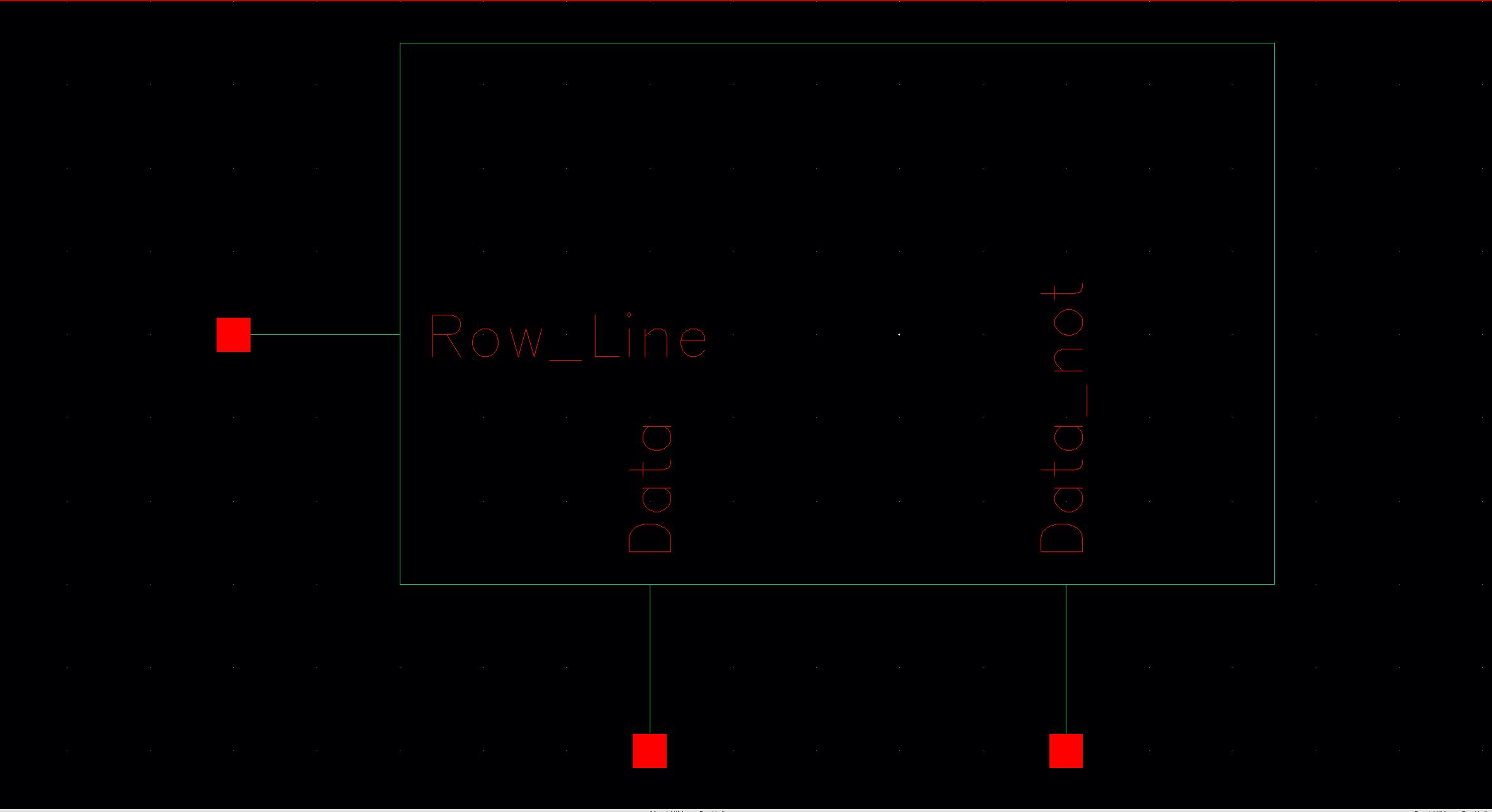
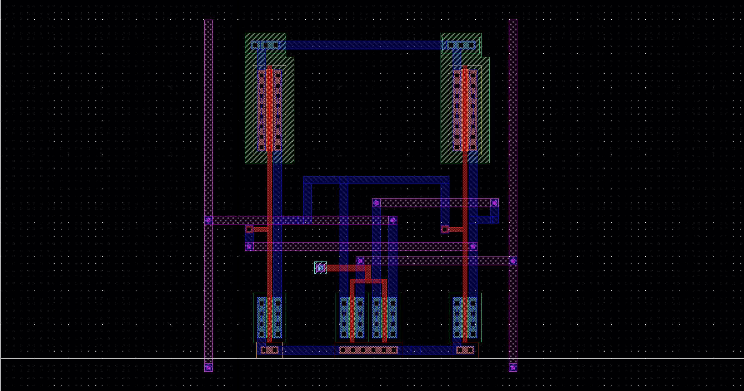
creating the schematic and the symbol for the bit cell I drafted a
layout and further created a standardized cell for instantiation. A
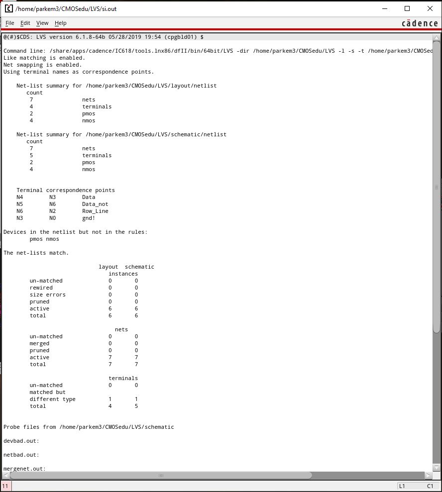
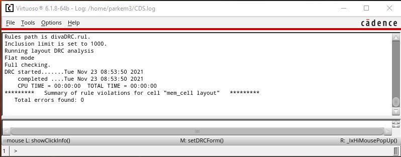
DRC, LVS,
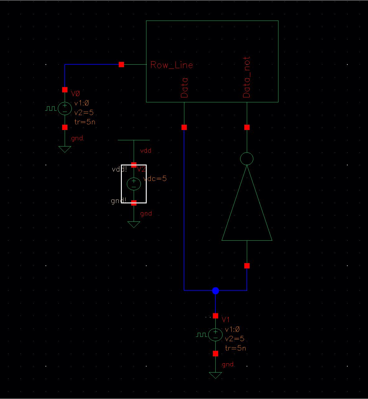
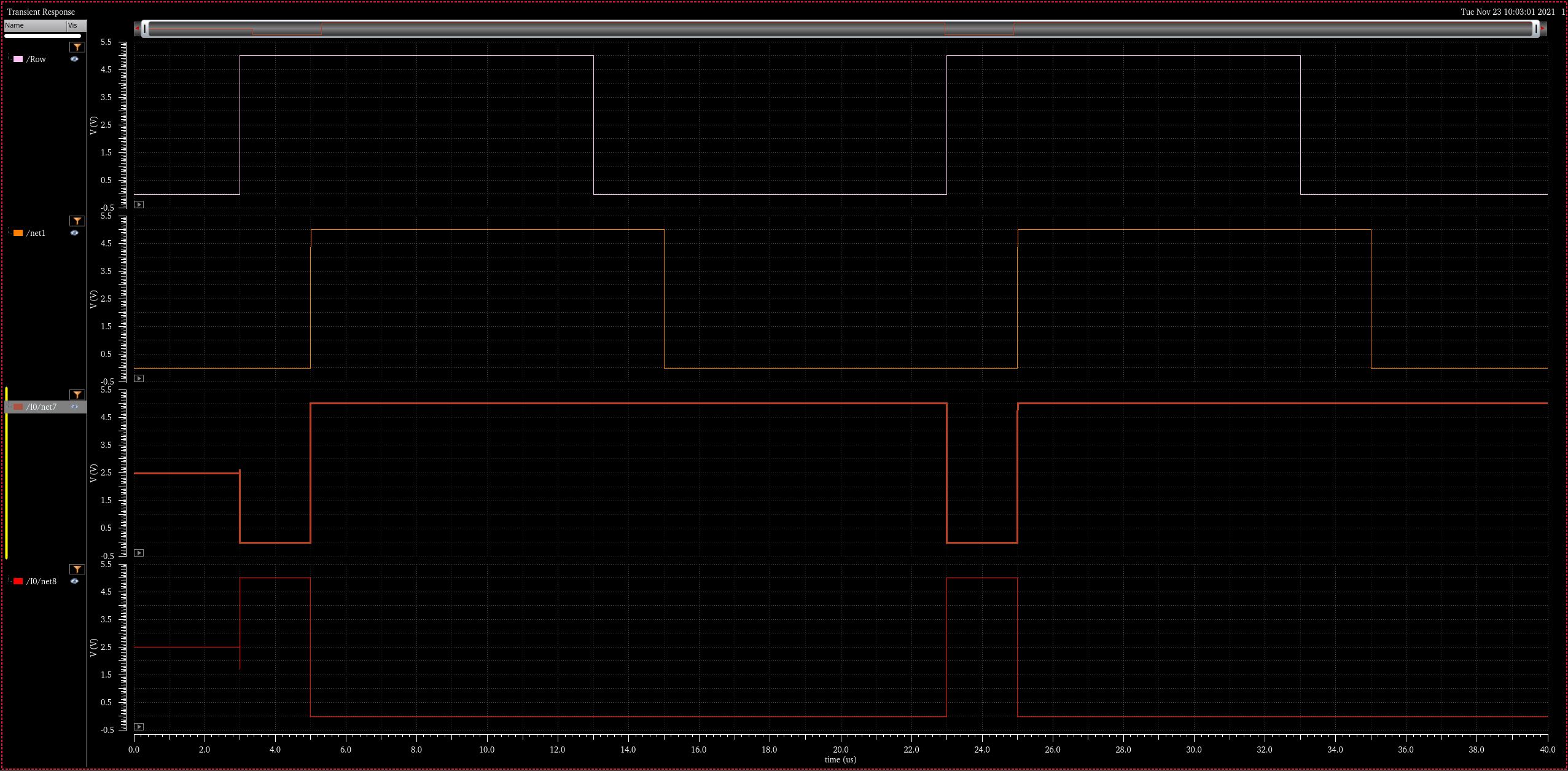
and a simulation were run to ensure that the cell was properly writing and holding data.
Word Cell
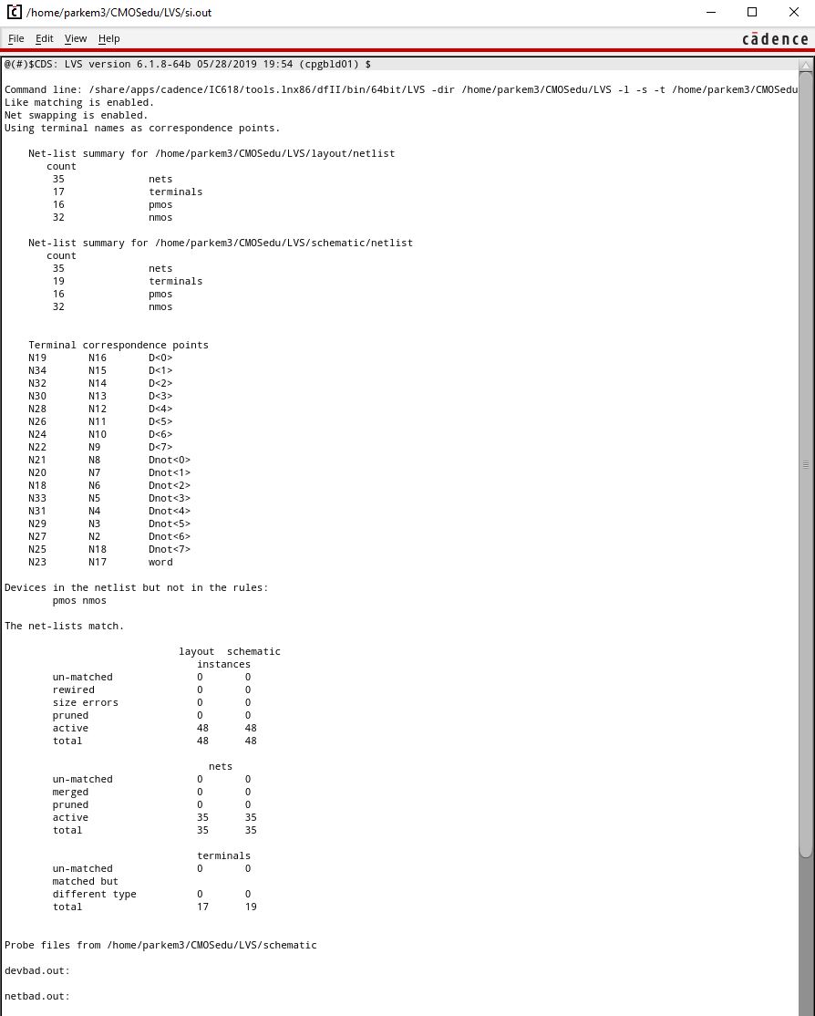
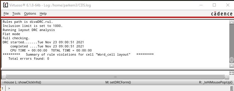
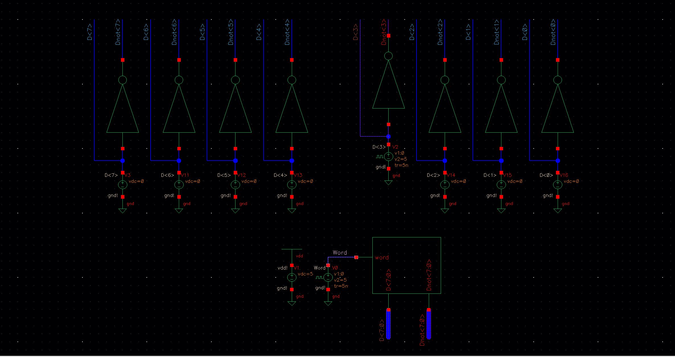
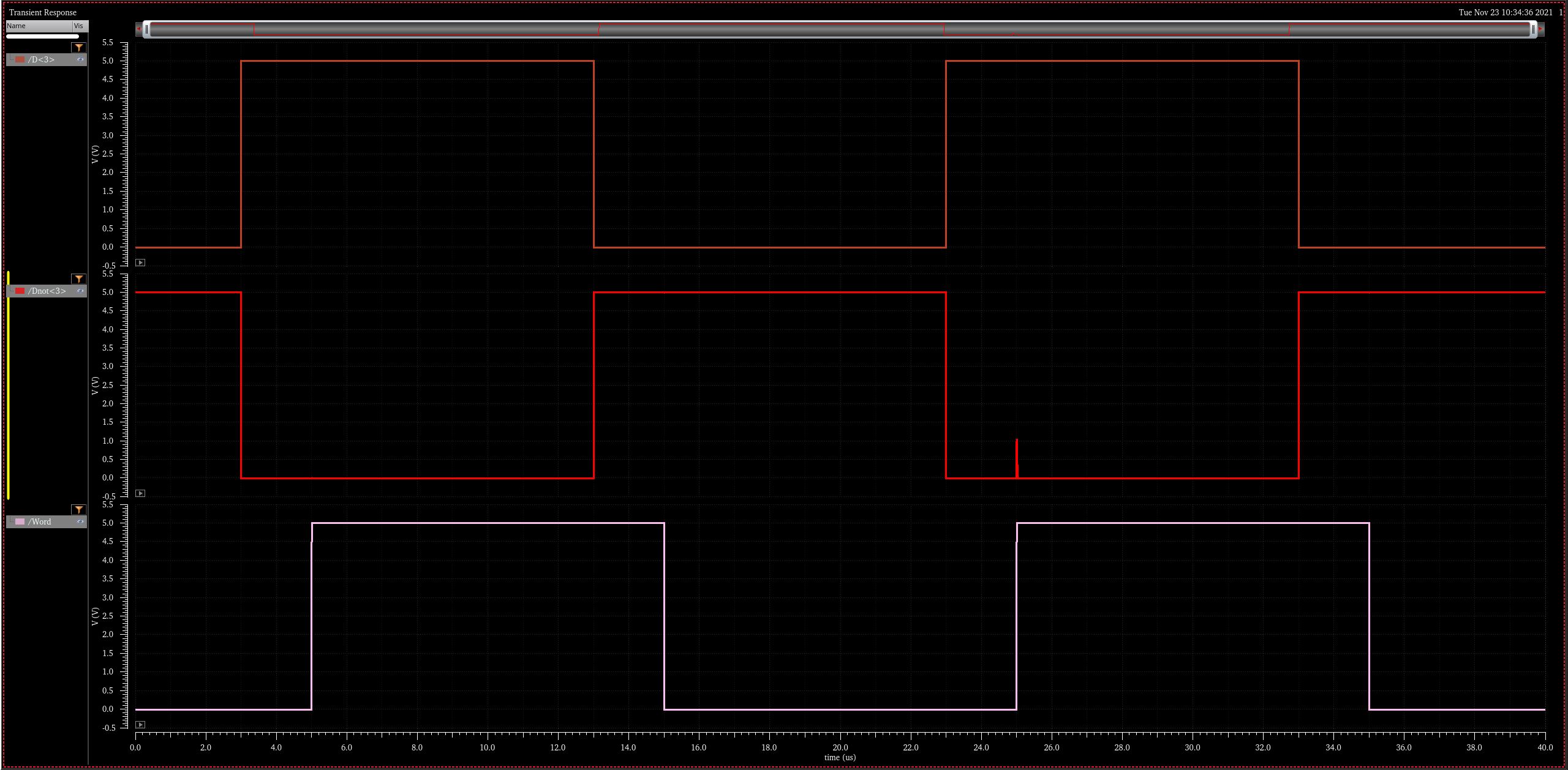
Now that the bit cell was finished I was able to instatiate it 8 times creating and 8-bit word cell.
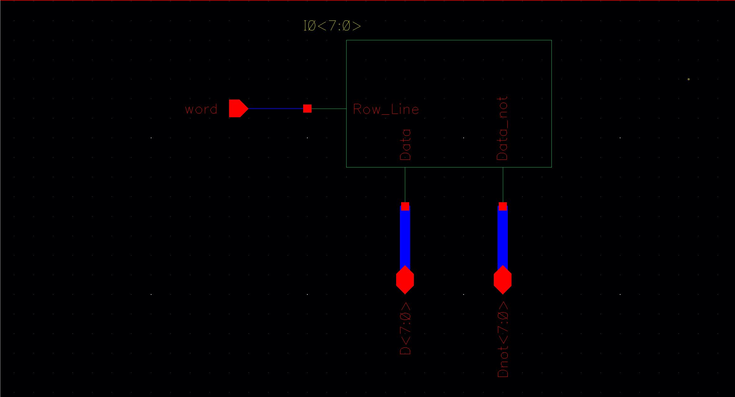
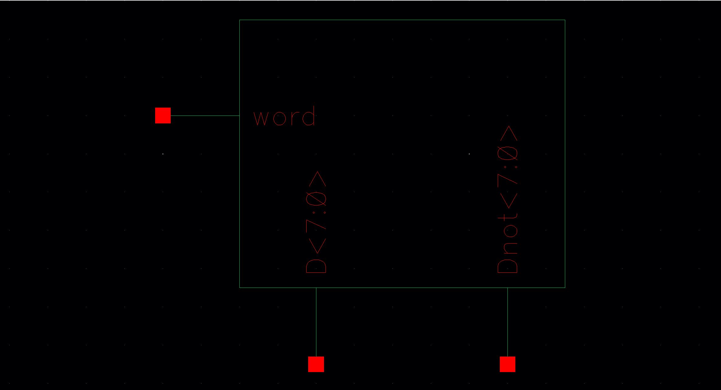
The
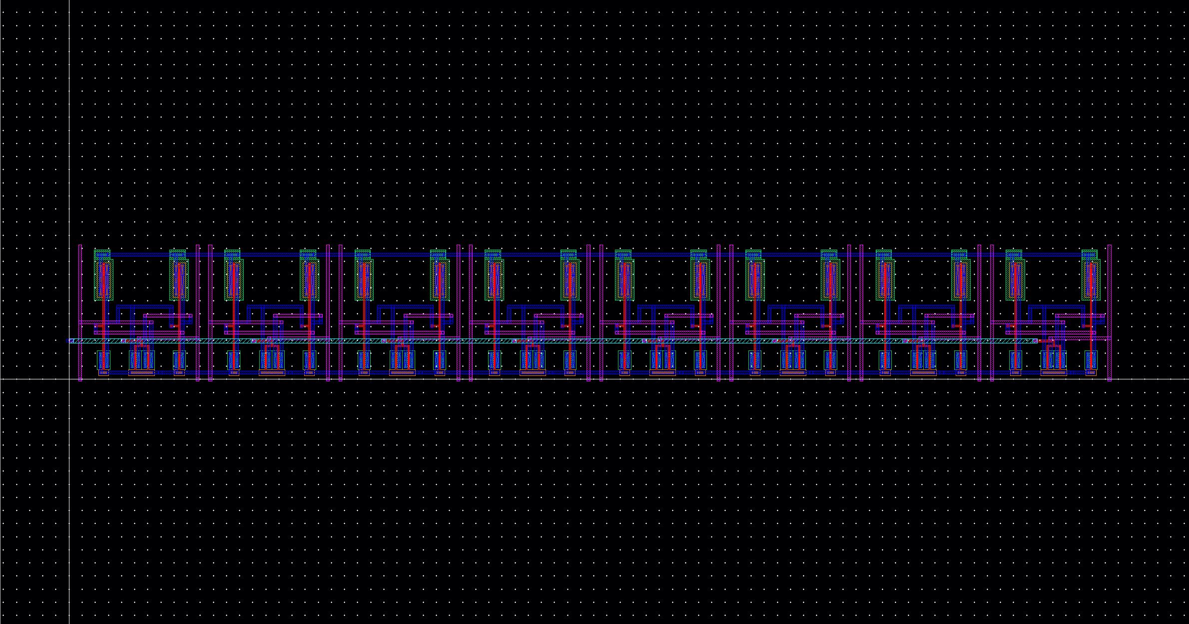
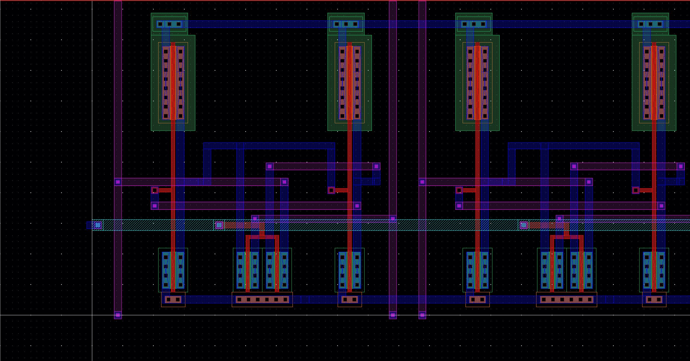
Layout of the cell was made easier by the use of a standardized cell
and linking the instantiations together on the M3 layer. This Layout
passed
DRC and LVS.
Array
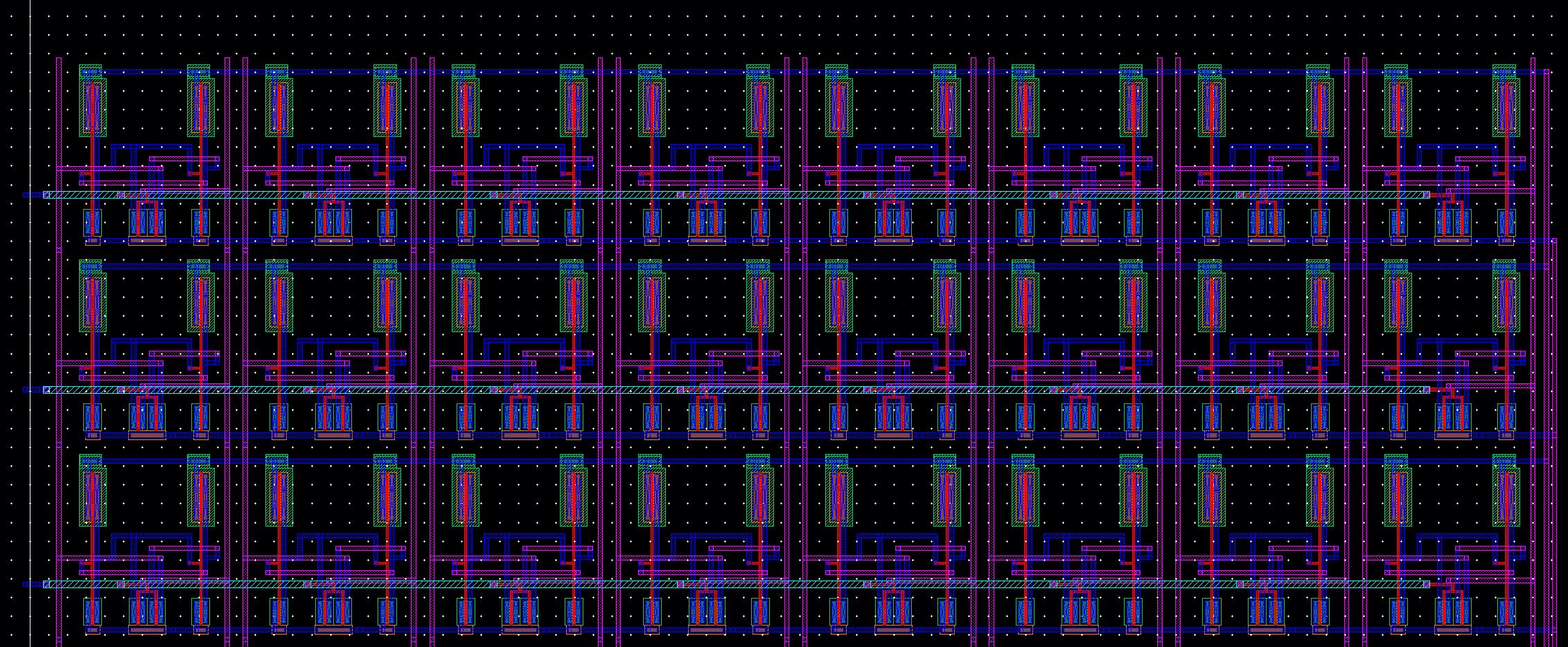
Word cells could now be instantiated to create a 32 word array.
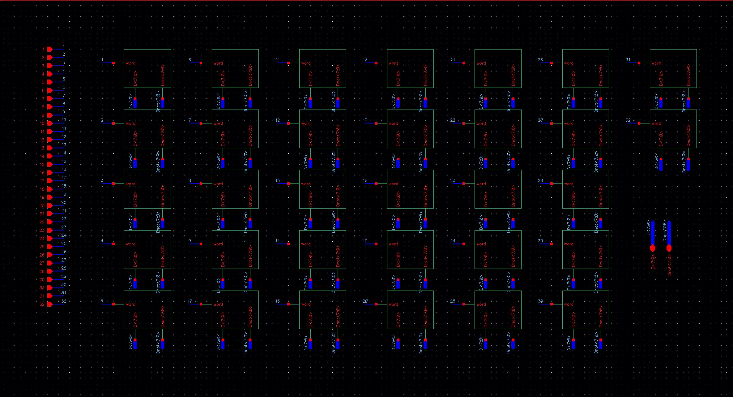
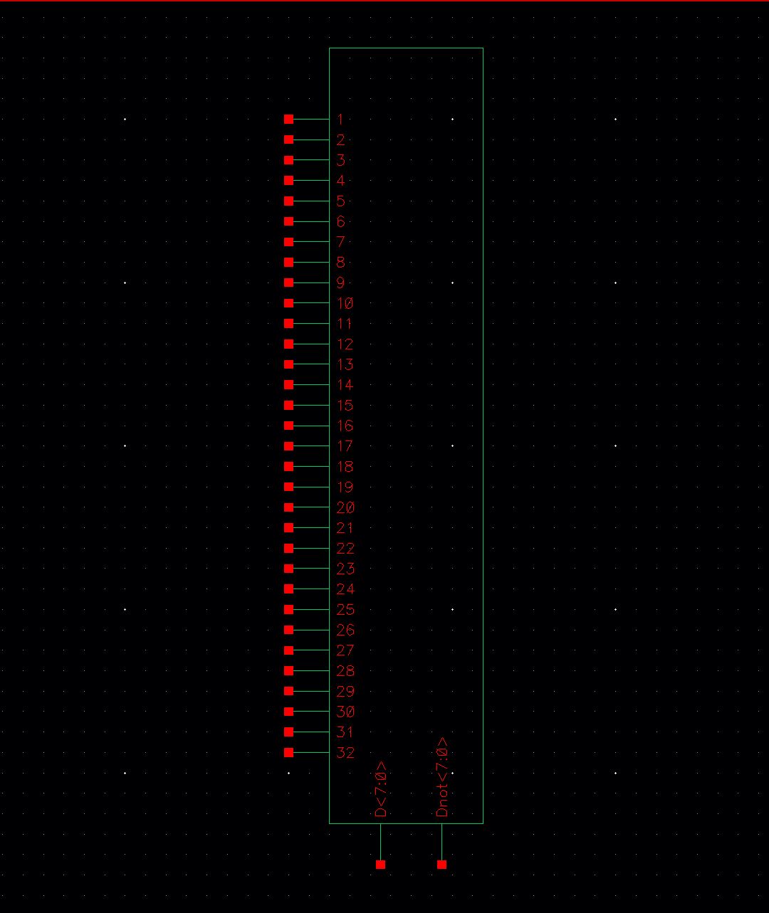
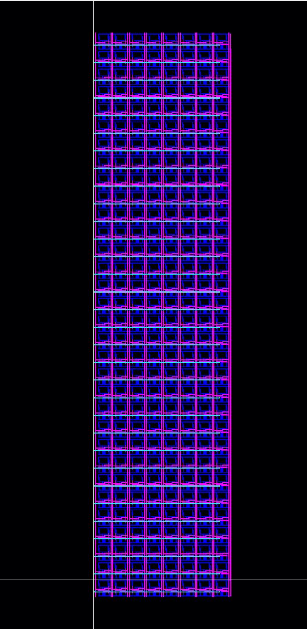
This array was linked through the use of two running M2 layers, one for VDD and one for ground.

NAND Gate
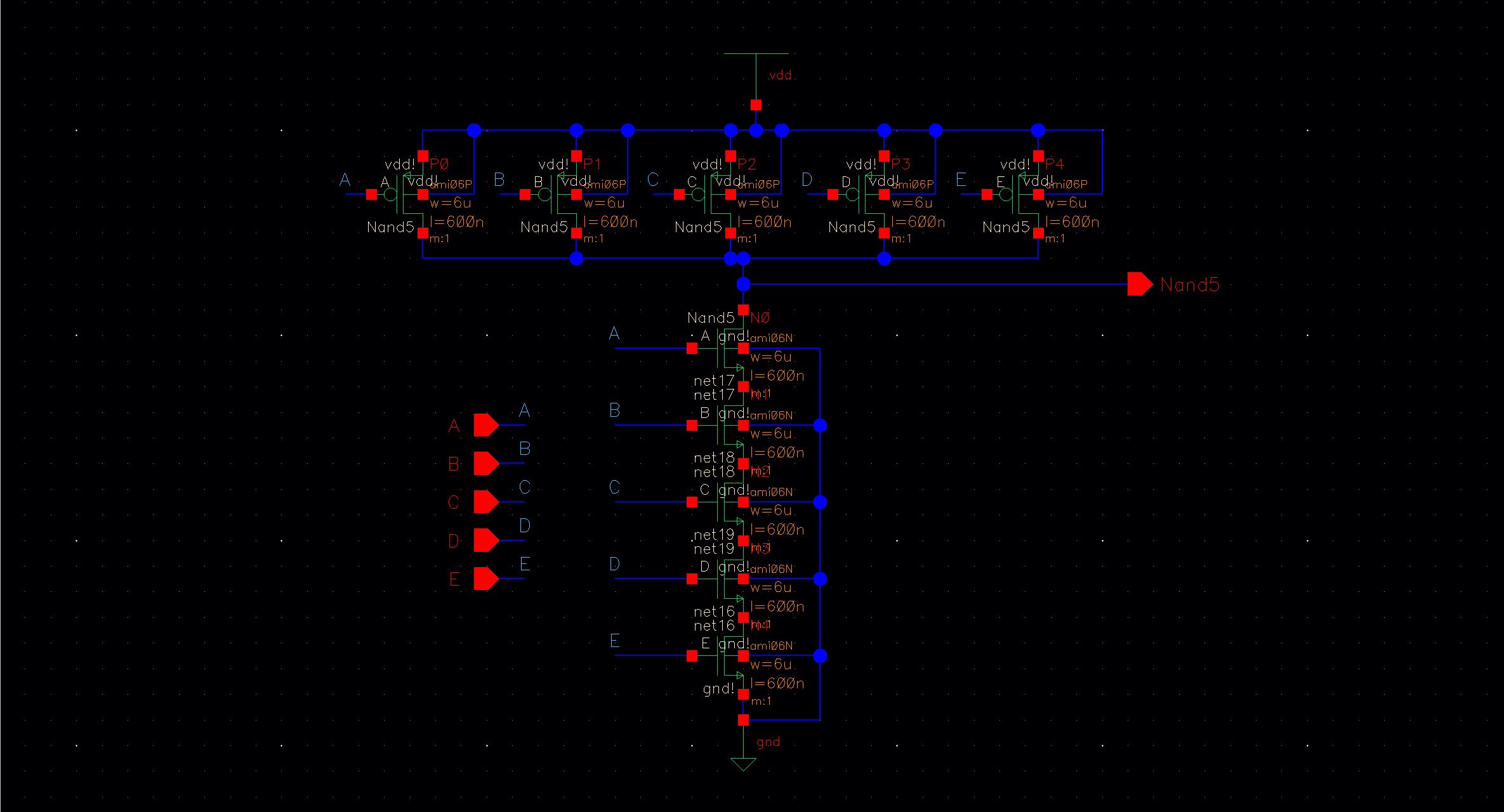
The next step was to draft the schematic for the needed 5 input nand gate. The schematic and symbol are shown below.

The
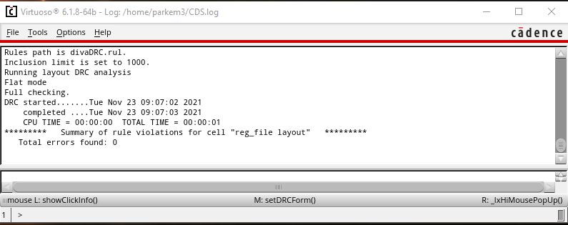
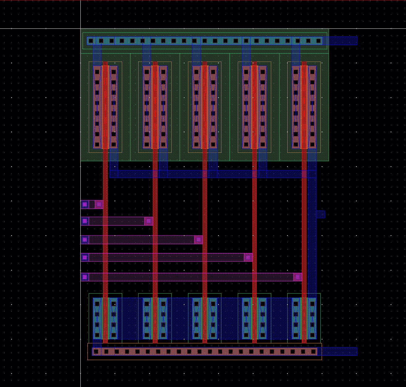
layout of the NAND gate was a slightly smaller cell size which through
off the allignment later in the project, but its design allowed for
easier
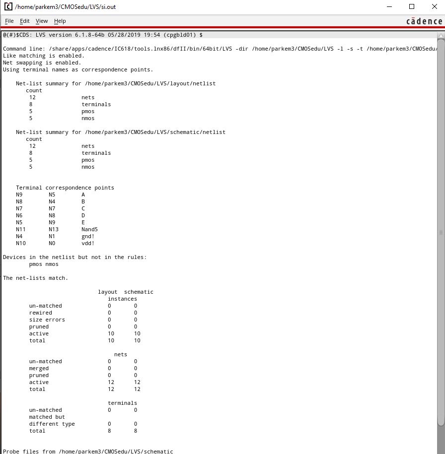
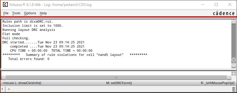
instantiation. The Layout passed both DRC and LVS.
Row Decoder
The
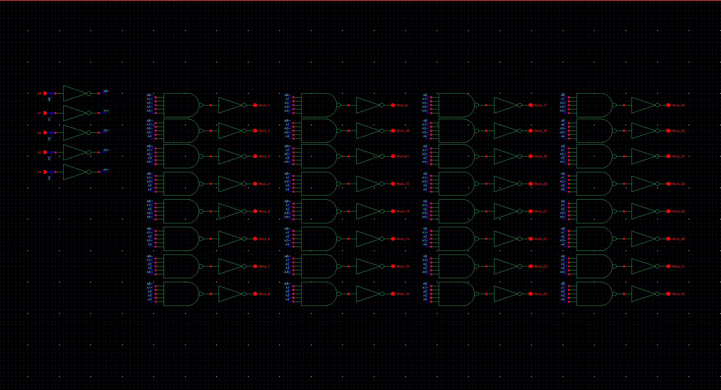
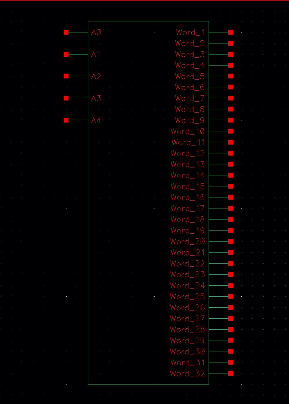
Row decoder was the next design to be tackled. This design uses
instantiations of 5-input NAND gates connected to inverters previously
drafted
to select our desired word.
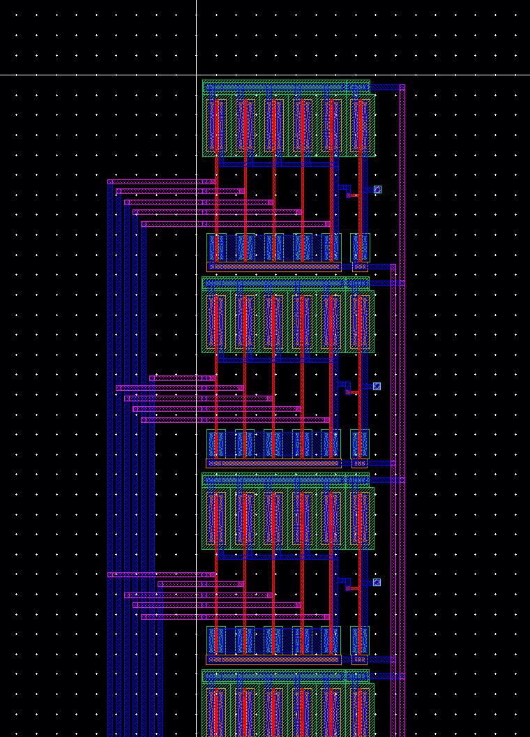
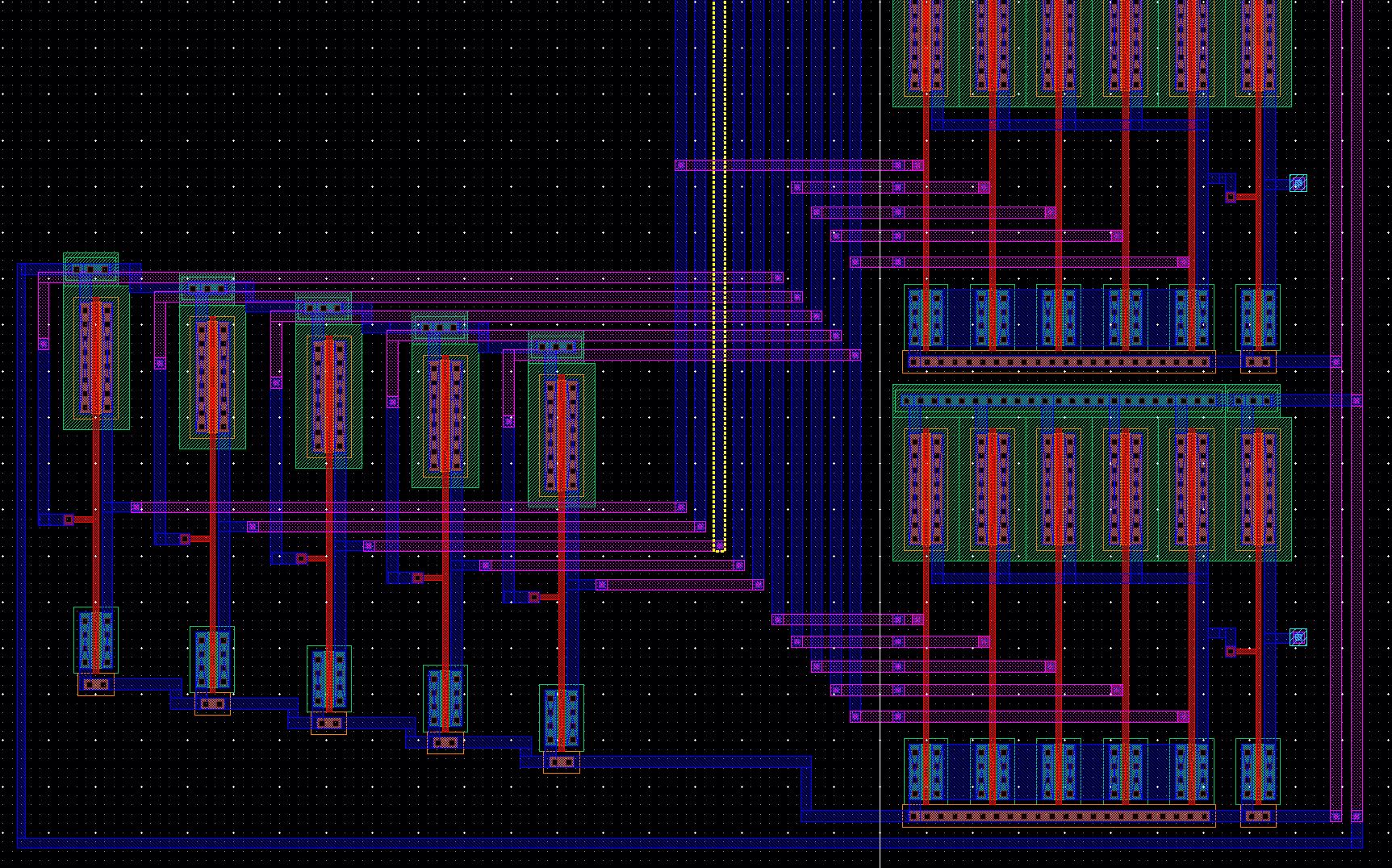
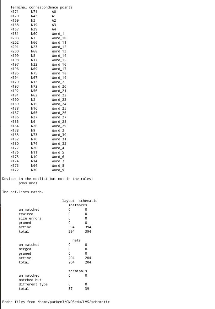
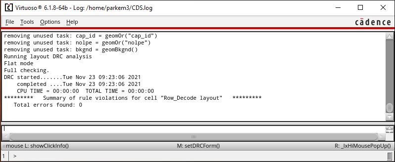
In
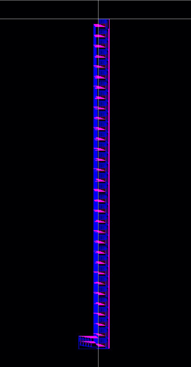
the layout I chose to use a bus configuration in order to efficiently
distribute my address information to the rest of the decoder. The
decoder
passed DRC and LVS.
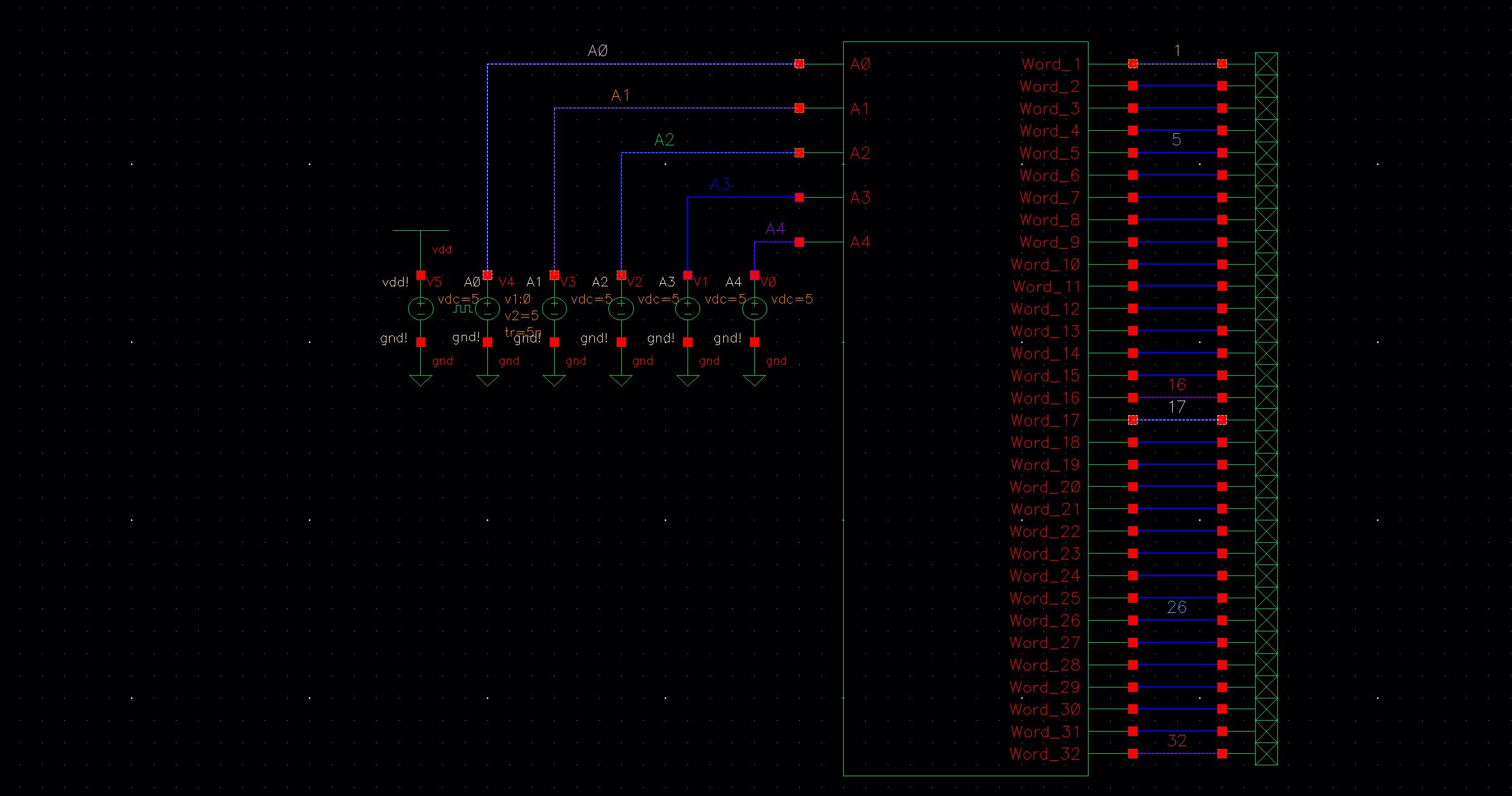
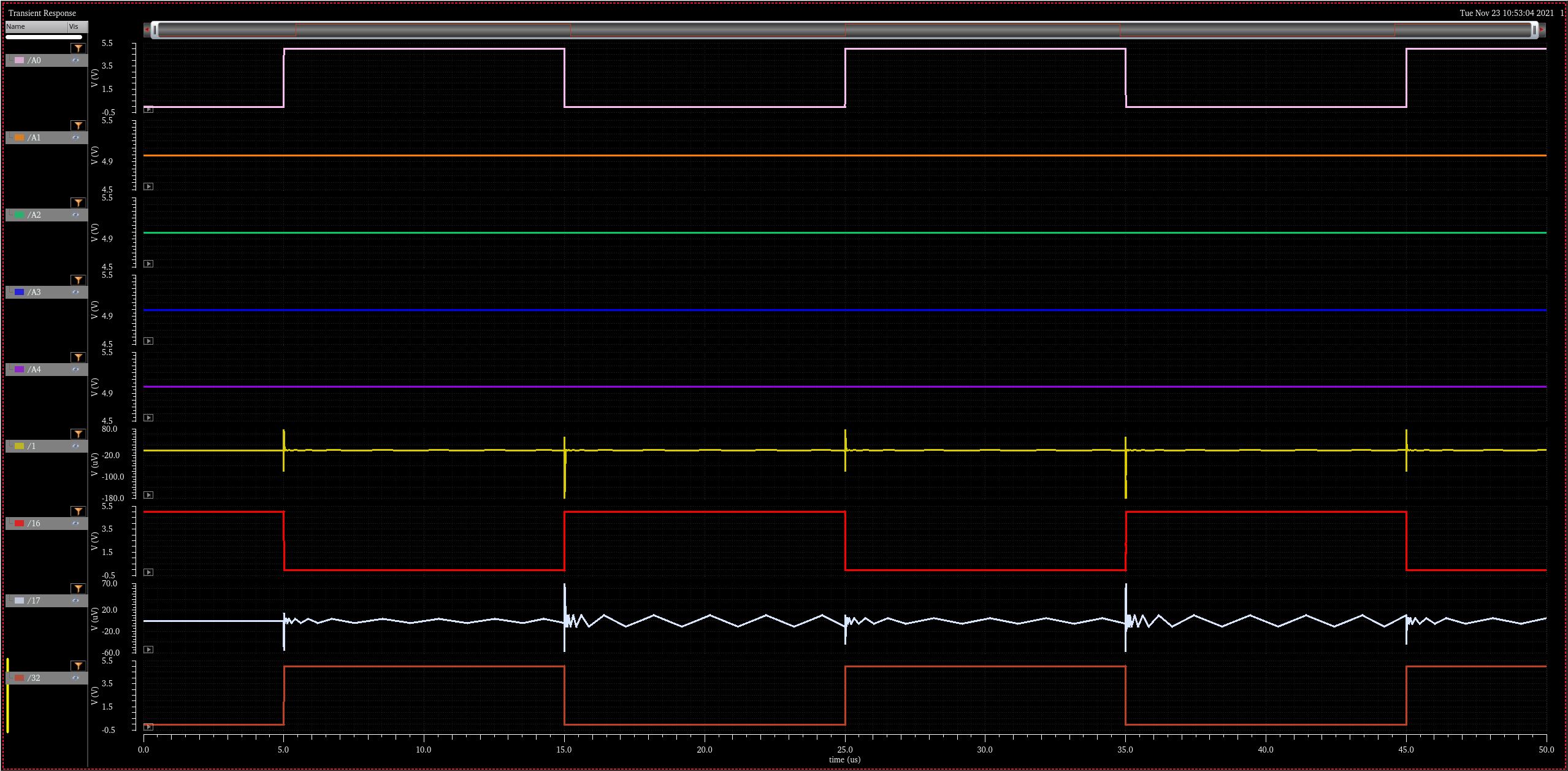
A
simulation was run to ensure that the decoder was properly selecting
the desired word line. This was accomplished by holding A<4:1>
constant and
toggling A<0>. This caused the enable on words 16 and 32 to toggle.
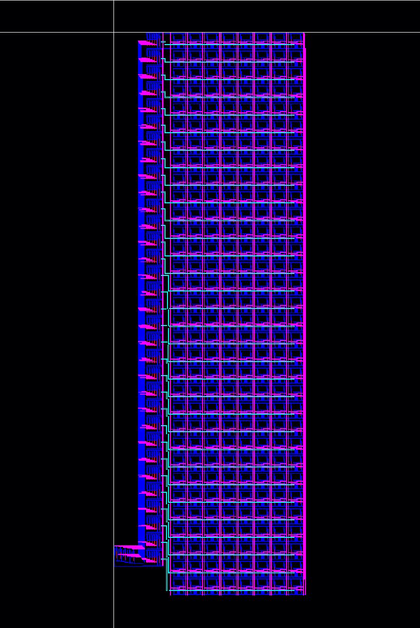
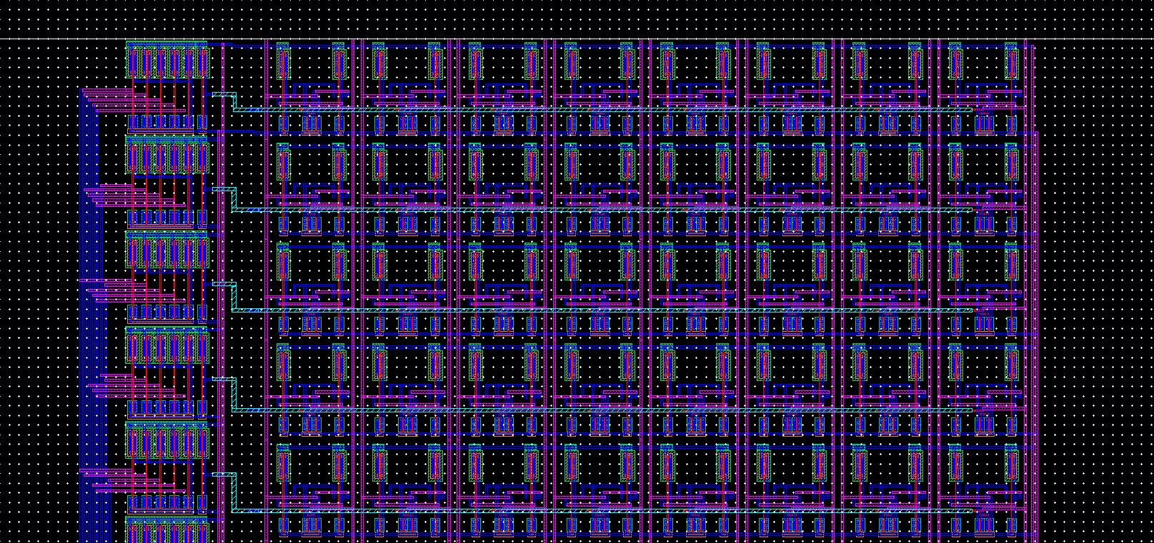
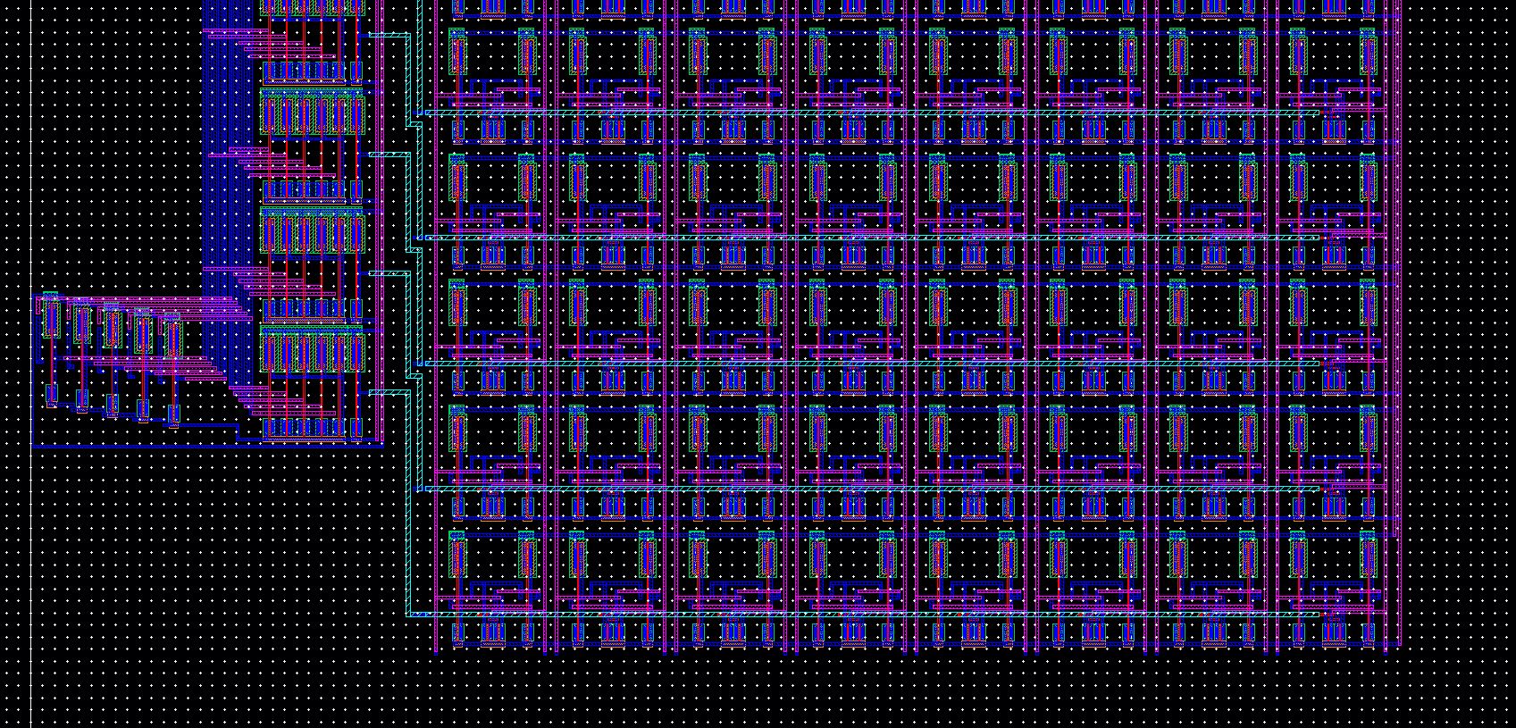
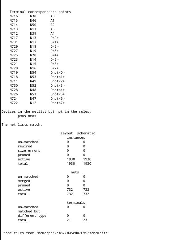
Final RF
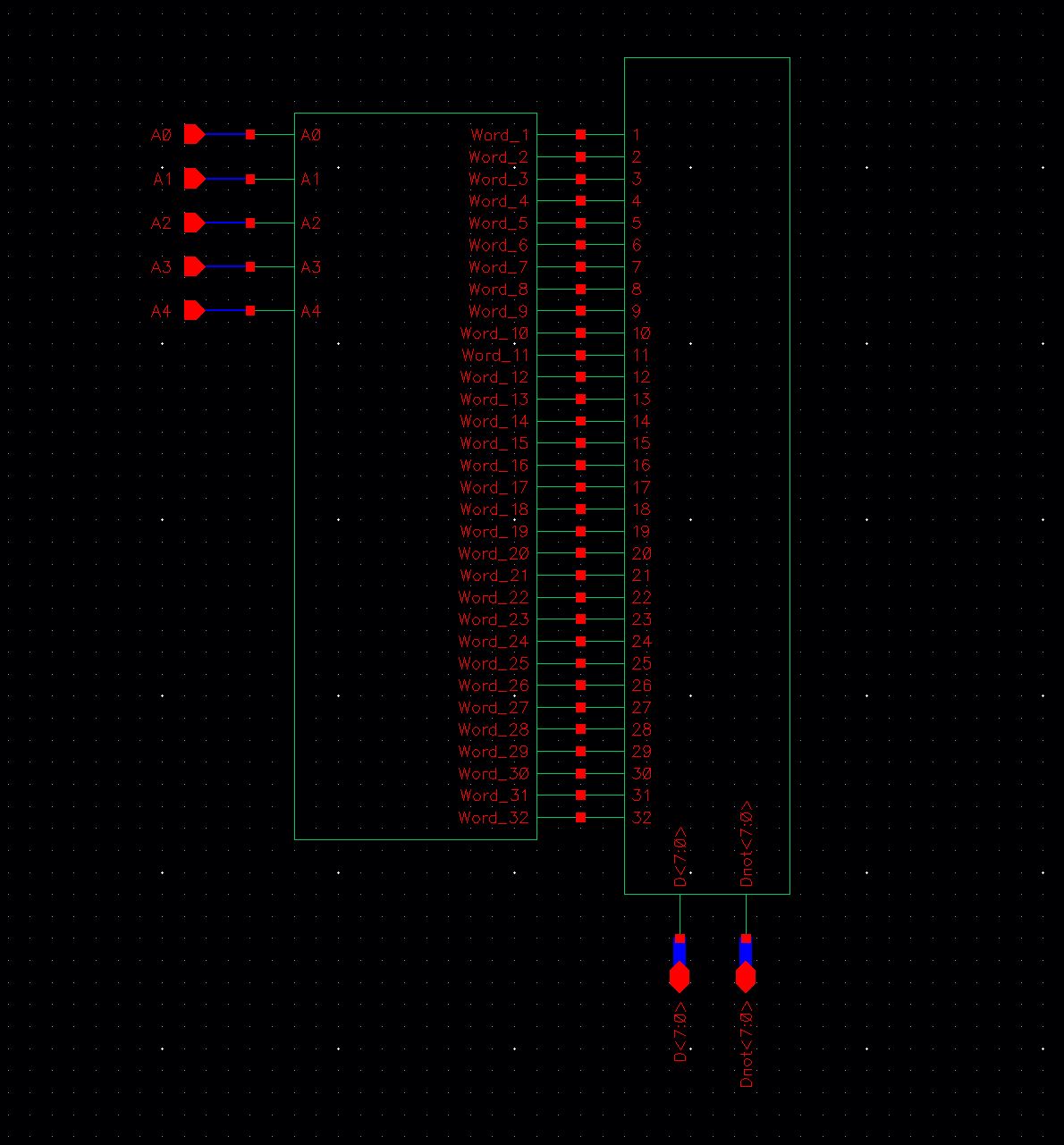
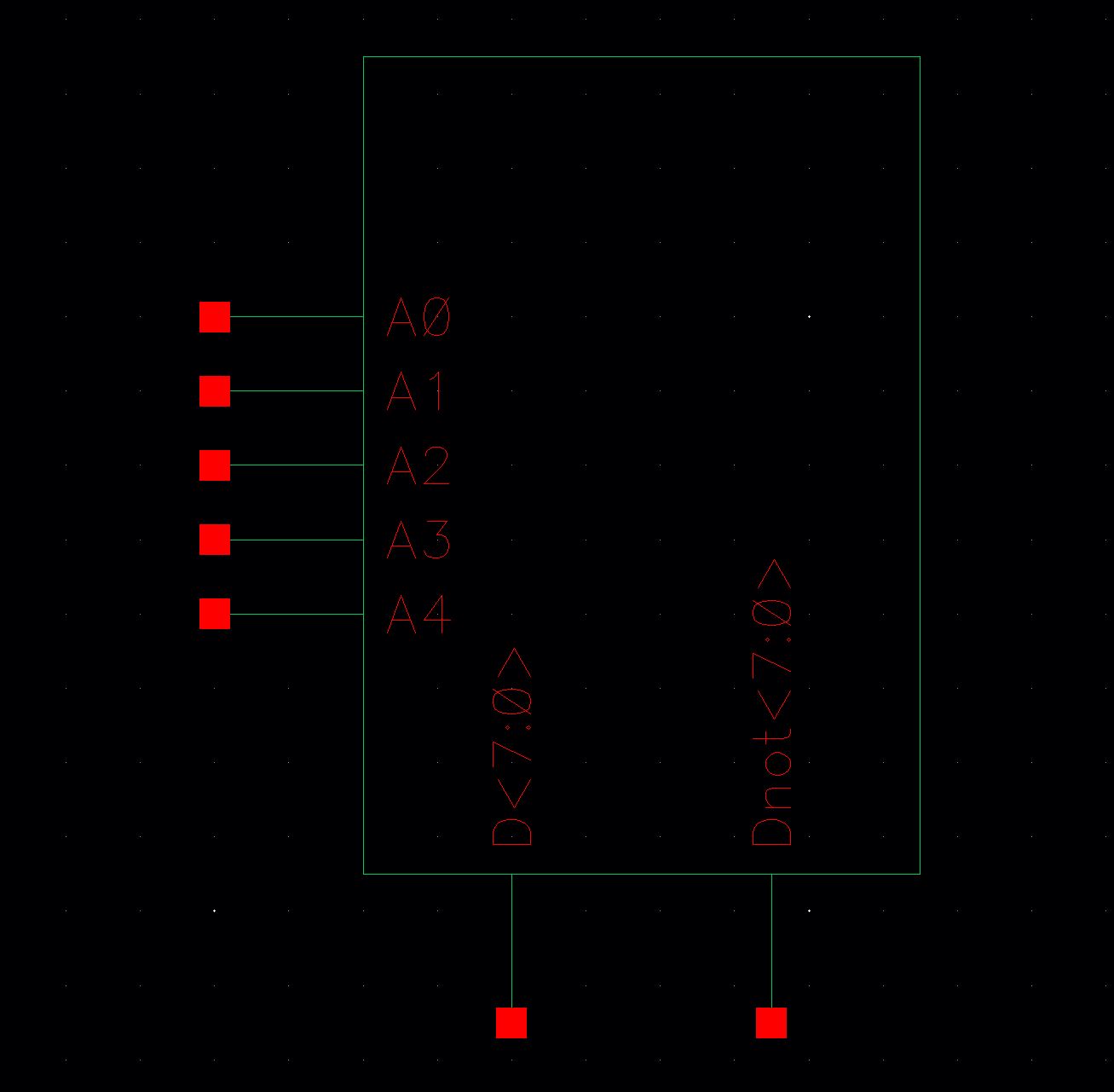
With
all of the independant elements complete I was able to combine the row
decoder and the memmory array into the final RF. This layout passed
DRC and LVS.

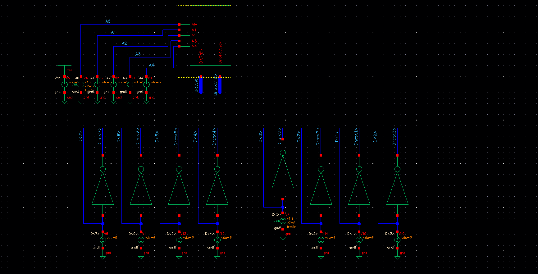
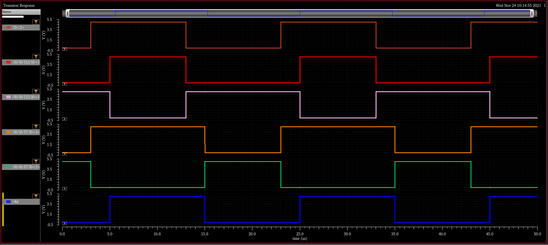
A simulation was done that shows writing and holding on bit 3 of words 16 and 32.
Design files can be downloaded here.