Lab 2 – Design 10-bit DAC (digital-to-analog converter)
EE 421L Digital IC Design
By: David Nakasone – Email: nakasd3@unlv.nevada.edu
Assigned: September 1, 2021
Due: September 8, 2021
Lab description >>>
This lab exposes the student to
digital-to-analog converters (DACs) and analog-to-digital converters
(ADCs). CMOS technology provides several important implementations of
these devices. Implementation is achieved with the R-2R ladder.
There are two major tasks for this lab:
A) preparations
B) design
Part A : preparations >>>
[ 1 ] following the tutorial
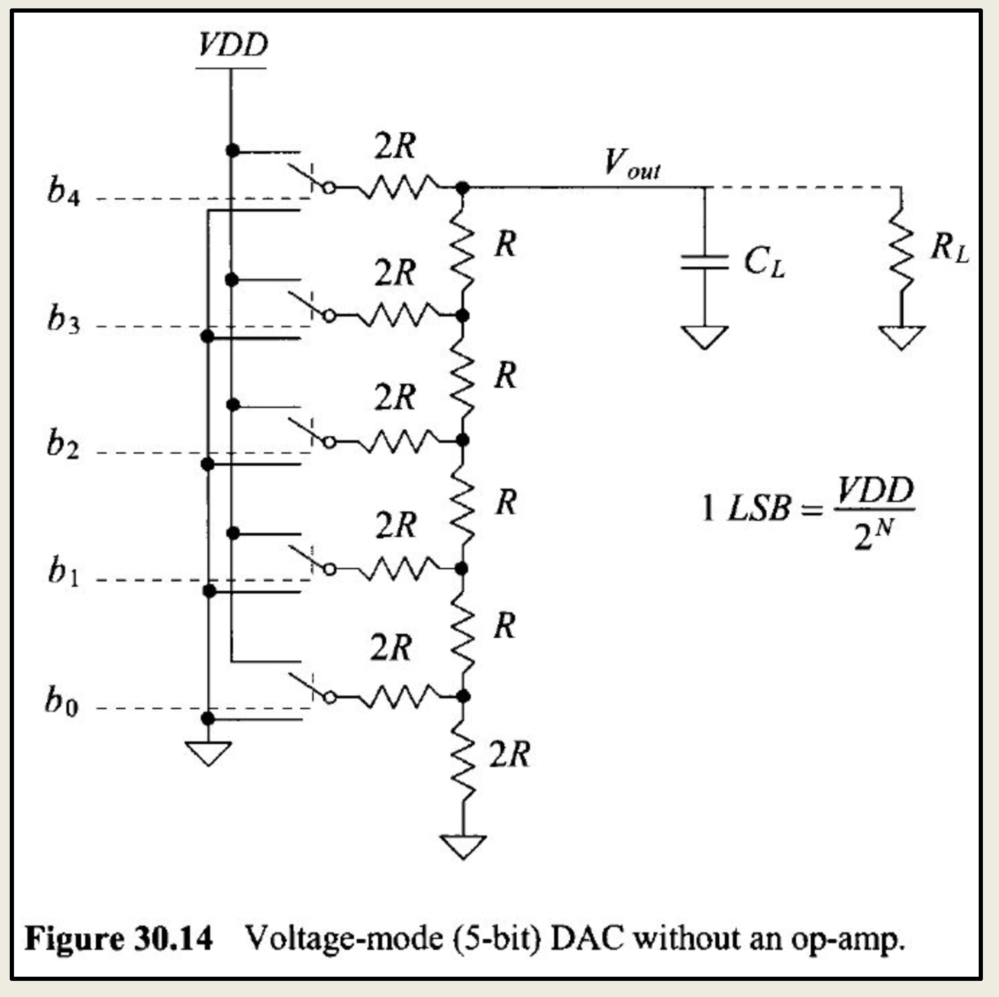
[ 2 ] theoretical behavior
[ 3 ] normal operation
[ 4 ] out of range, cut-off
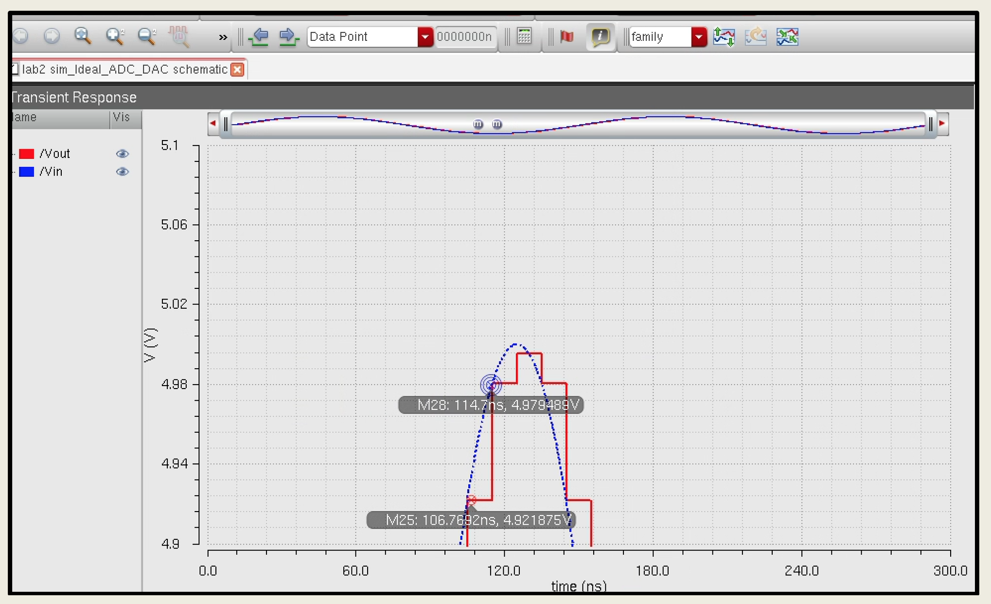
For lab2, we will use the simplified version, LSB (as minimum voltage to change output of ADC -> 1 LSB = V_DD / 2^10
Examining the step size, 1 LSB = 5 / 2^10 = 4.882 mV :
This device can represent 2^10 = 1024 unqiue values
Part B : design>>>
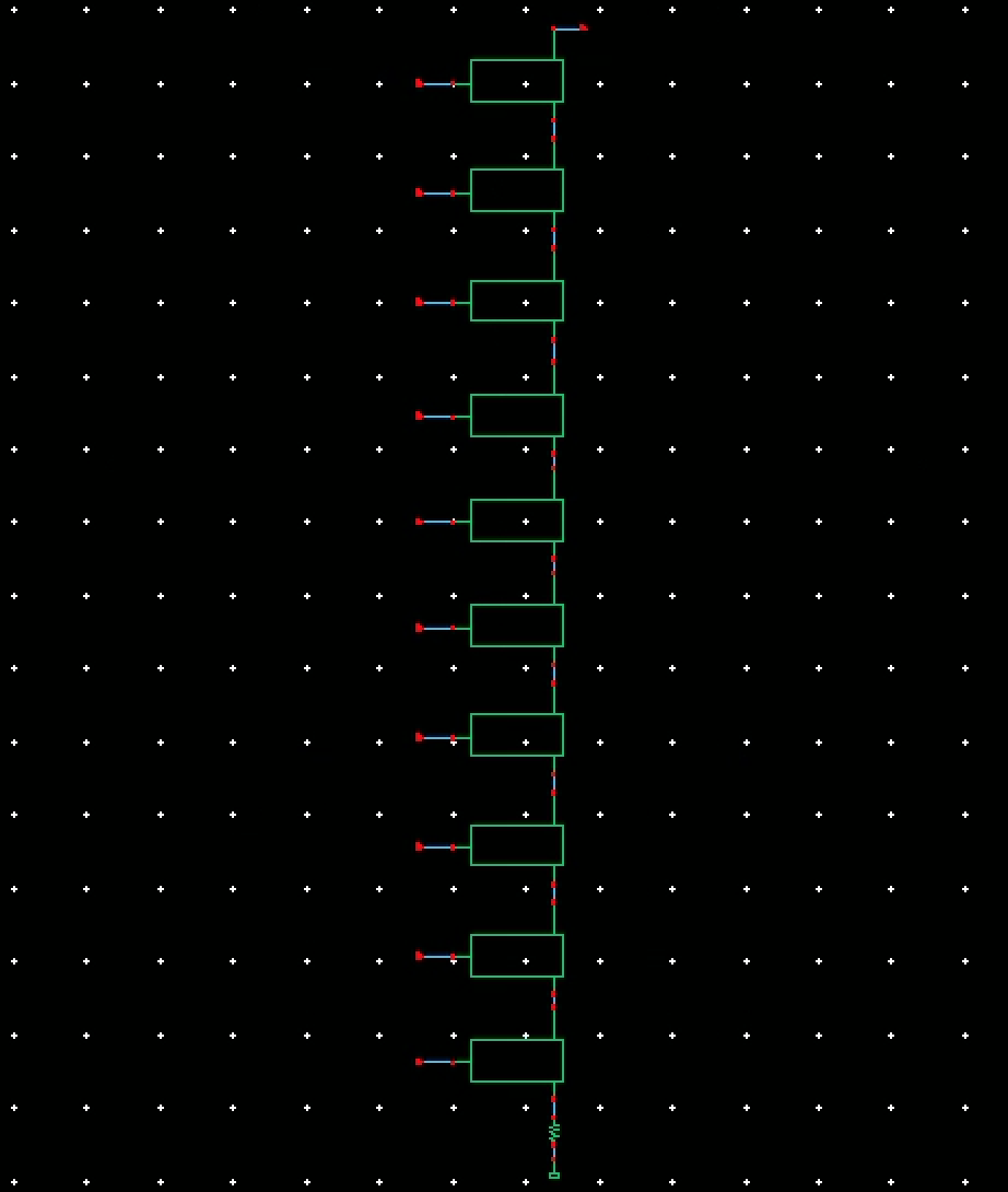
[ 1 ] create the schematic following template, R = 10 kΩ
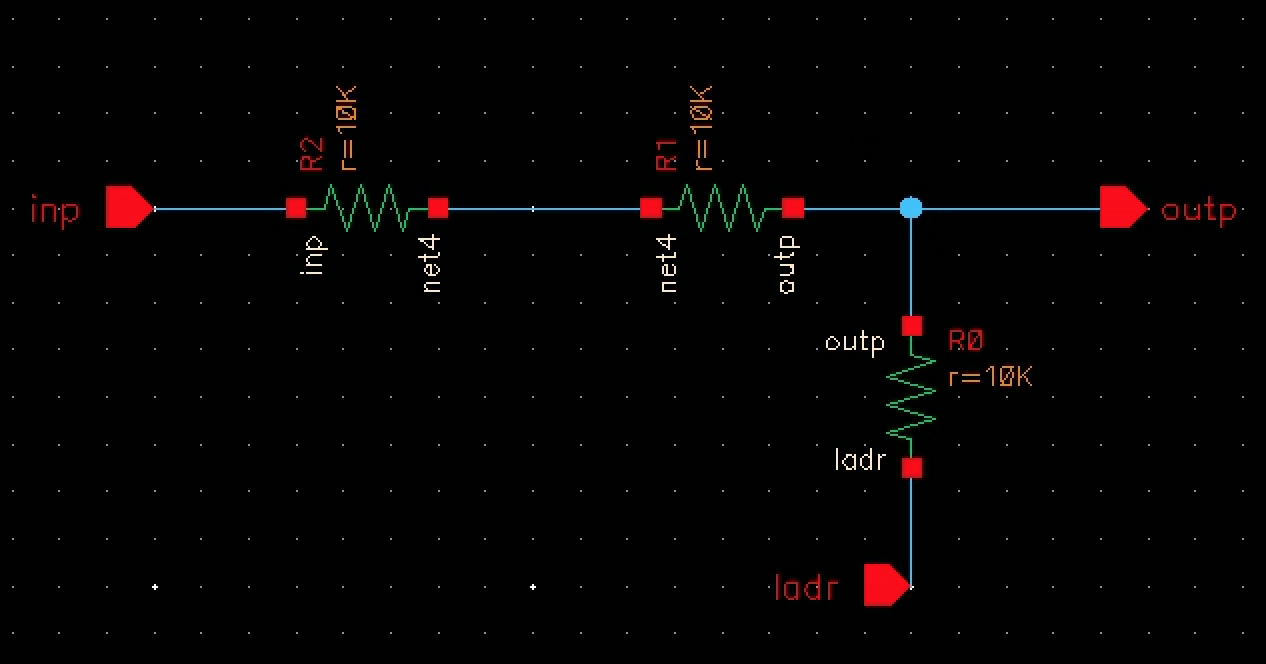
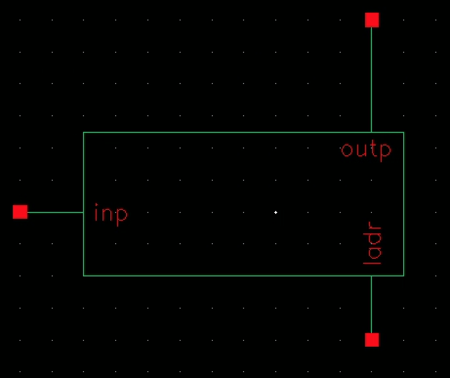
[ 2 ] This DAC uses a ladder of R-2R resistors, create a symbol to make the schematic
[ 3 ] Create a symbol of this ladder module to build the DAC
[ 4 ] In a new schematic, use this symbol to complete the DAC
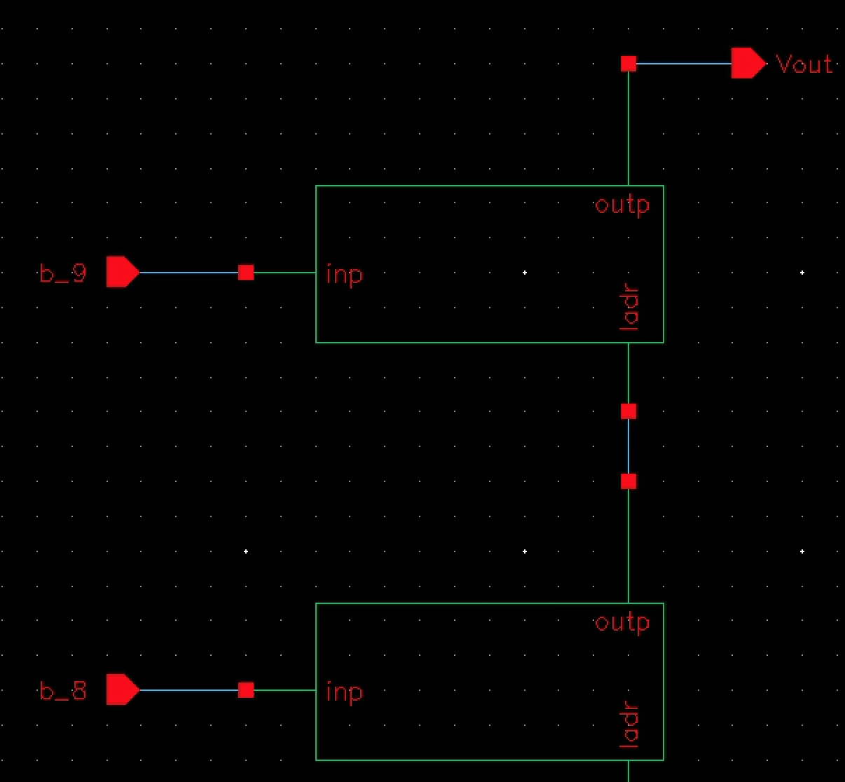
close up of top:
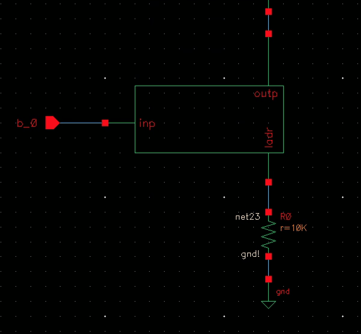
close up of bottom:
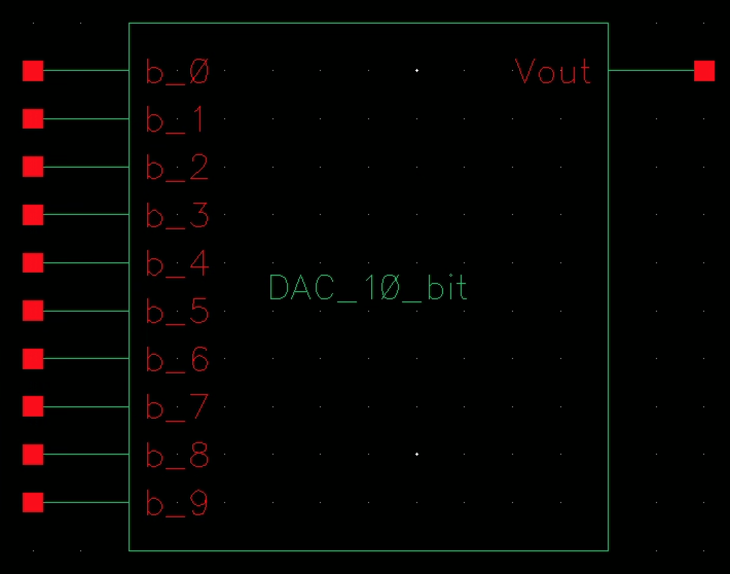
[ 5 ] Make a symbol of the DAC for testing
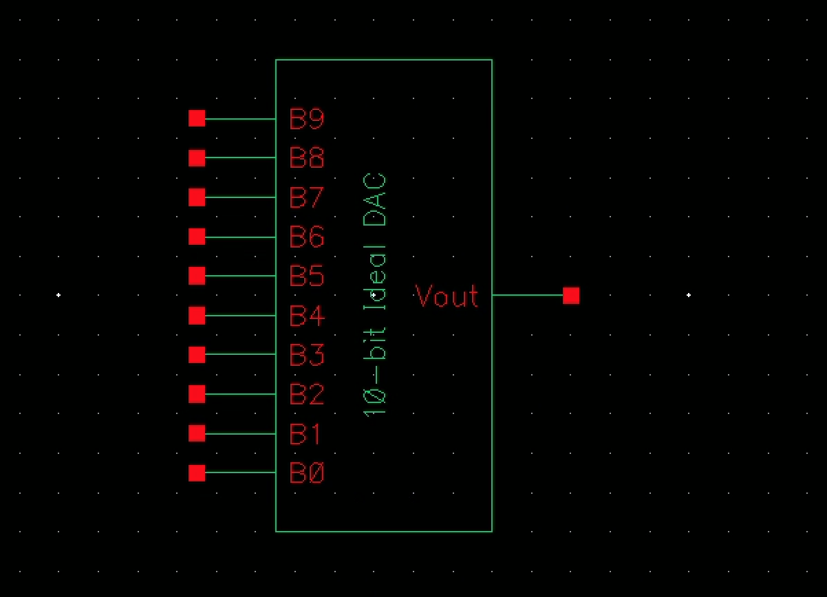
[ 6 ] Copy example "Ideal_10-bit_DAC" and remove VDD, Verfp, and Vrefm pins
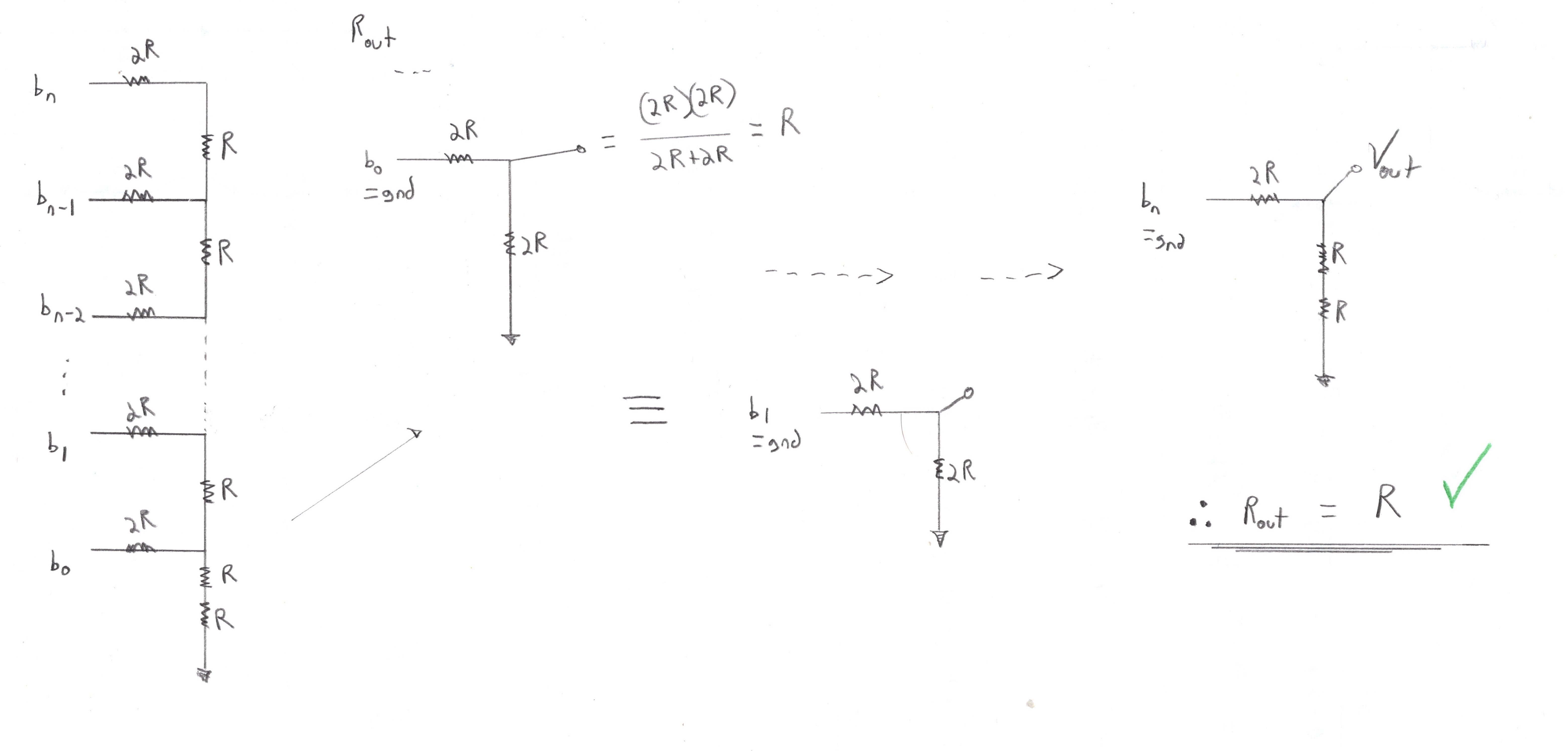
[ 7 ] Determine DAC output resistance by grounding all inputs and combing resistors
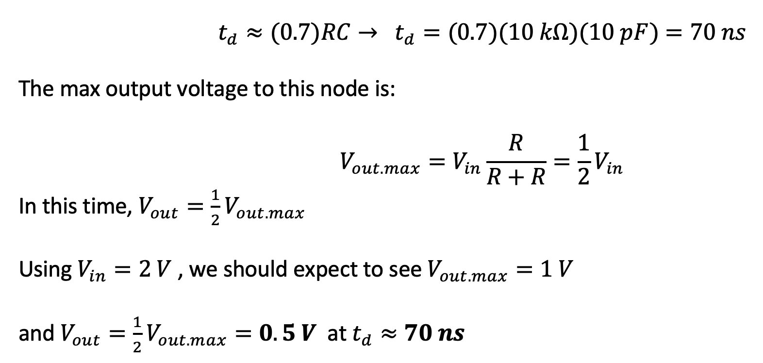
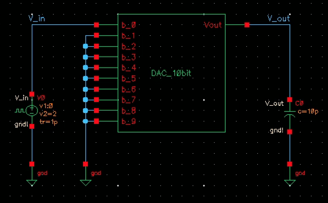
[ 8 ] Determine the delay with all pins grounded except B9, C = 10 pF
The DAC:
Equivelent Circuit:
Results, as expected:
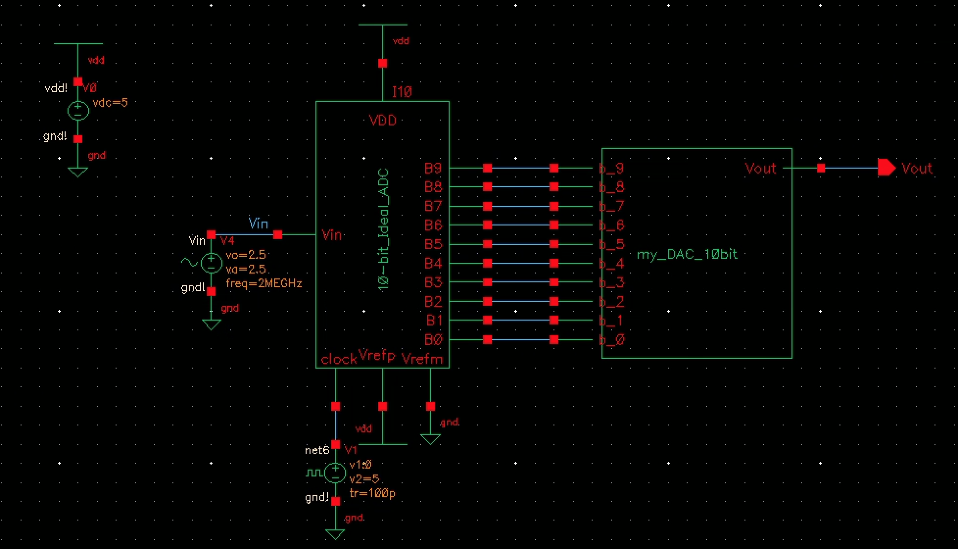
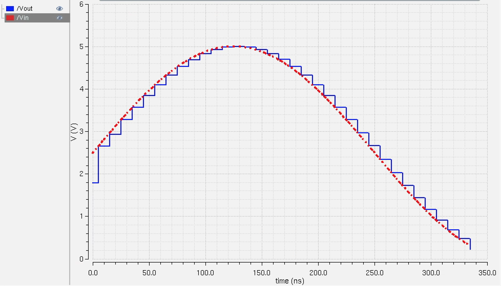
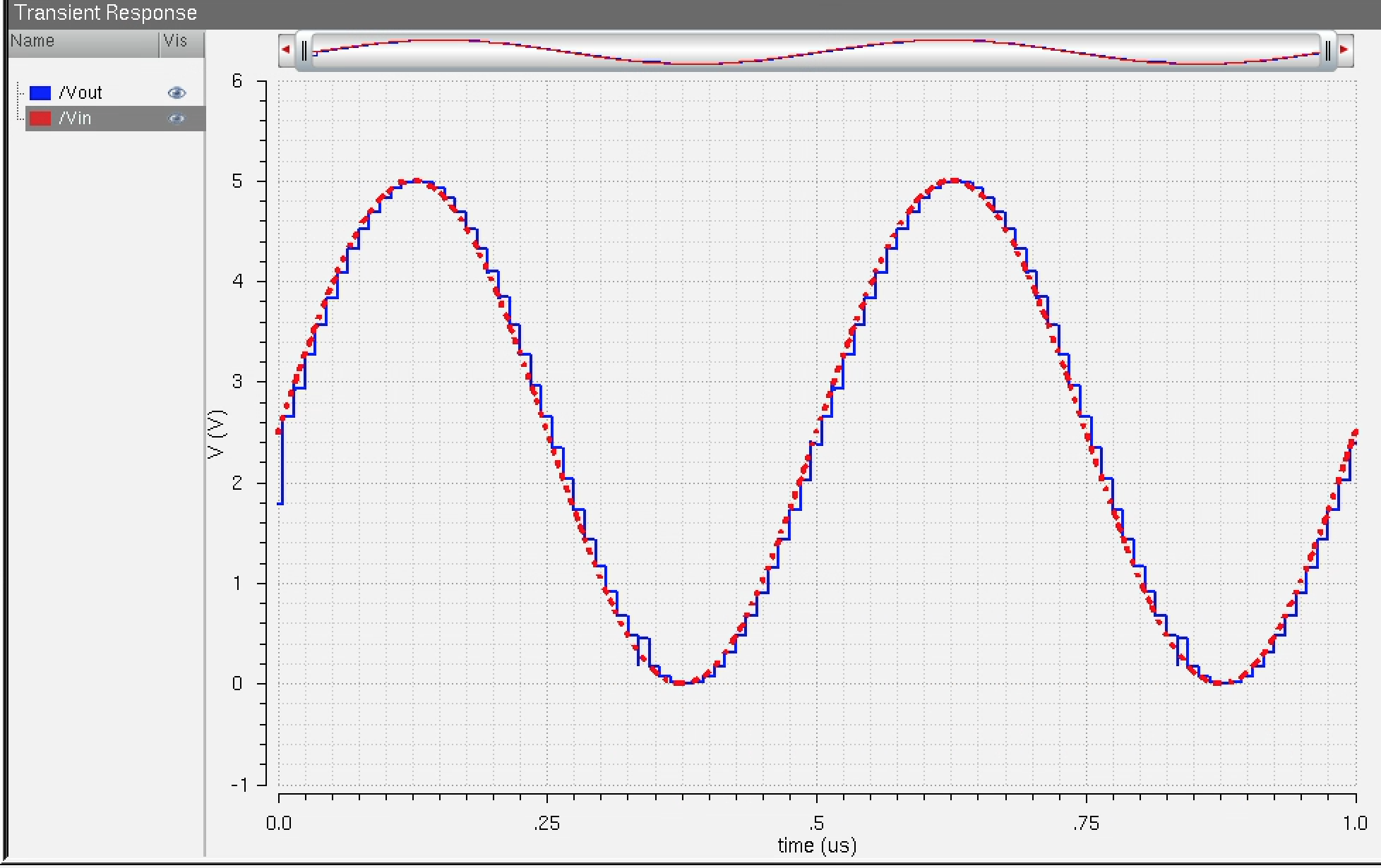
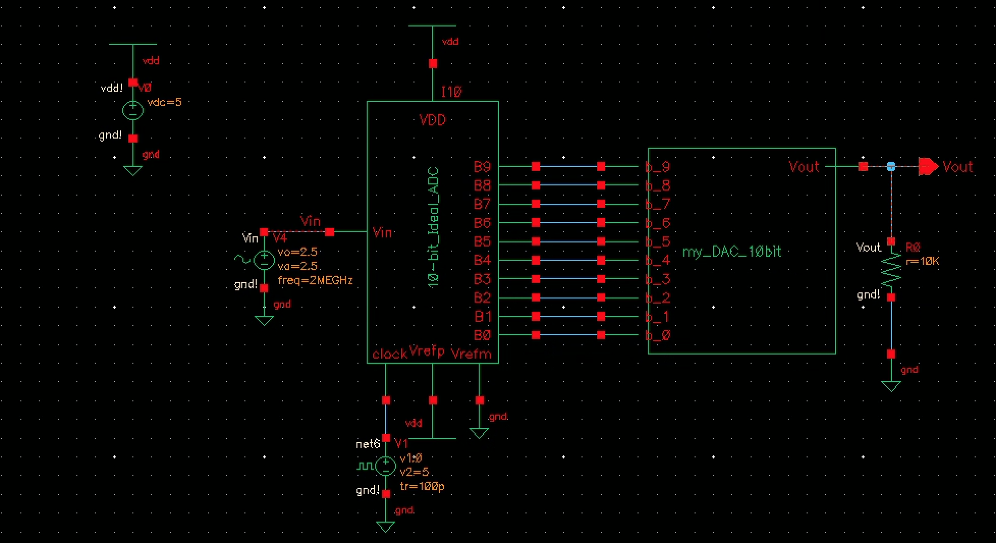
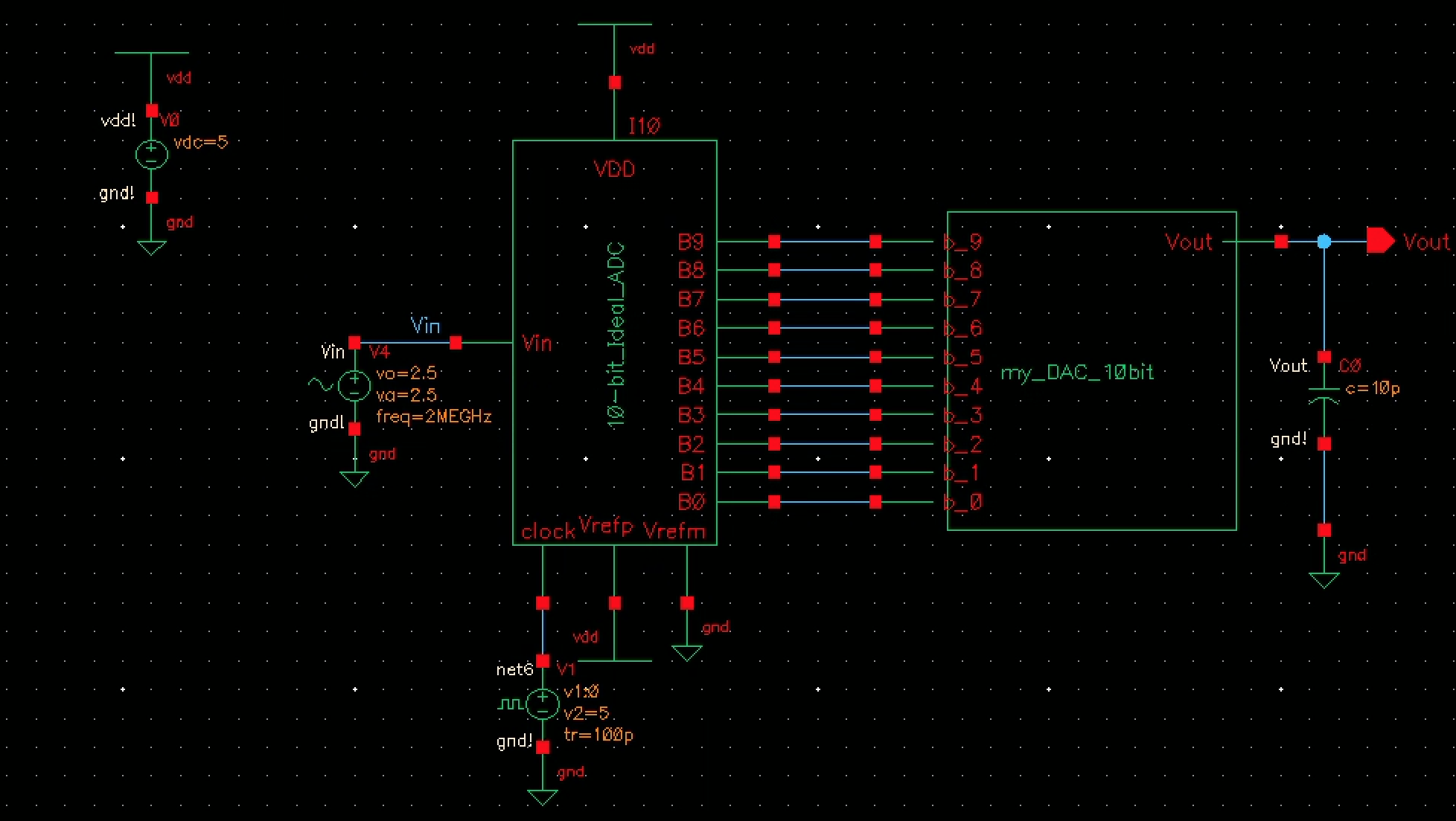
[ 9 ] copy "sim_Ideal_ADC_DAC" to cell "sim2_Ideal_ADC_DAC" ,
replace DAC with your design and ensure it works
Incomplete results
After correction (fix convergence issues by allowing more tolerance)
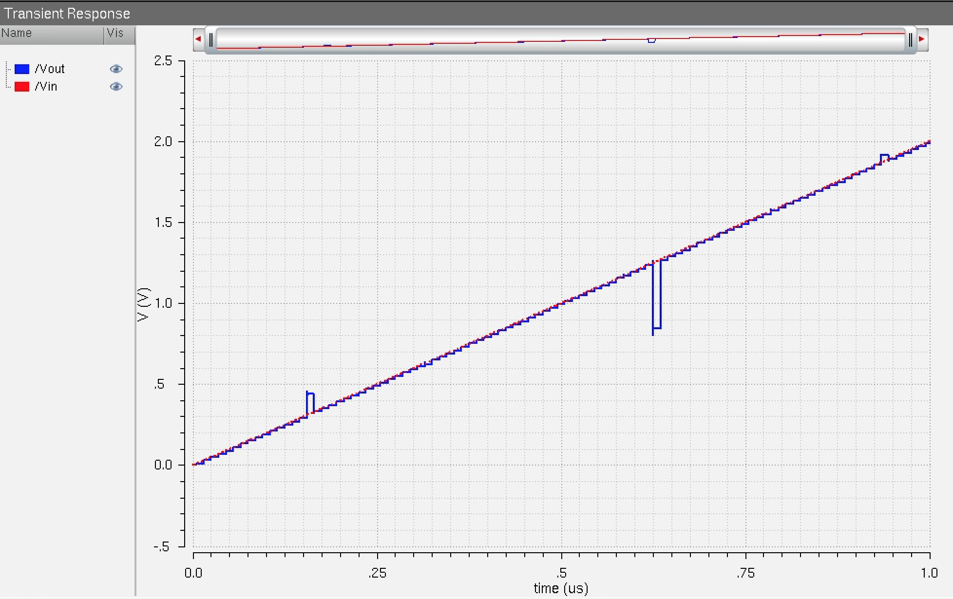
Finally, check with a ramp input
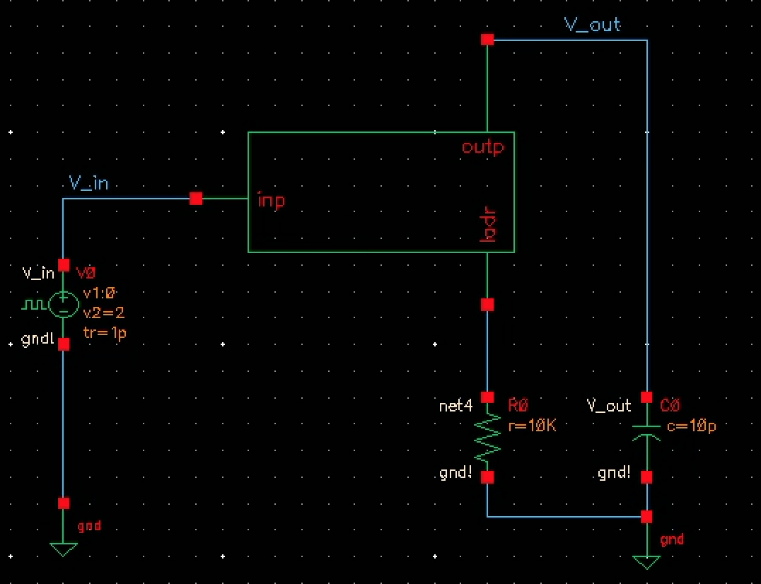
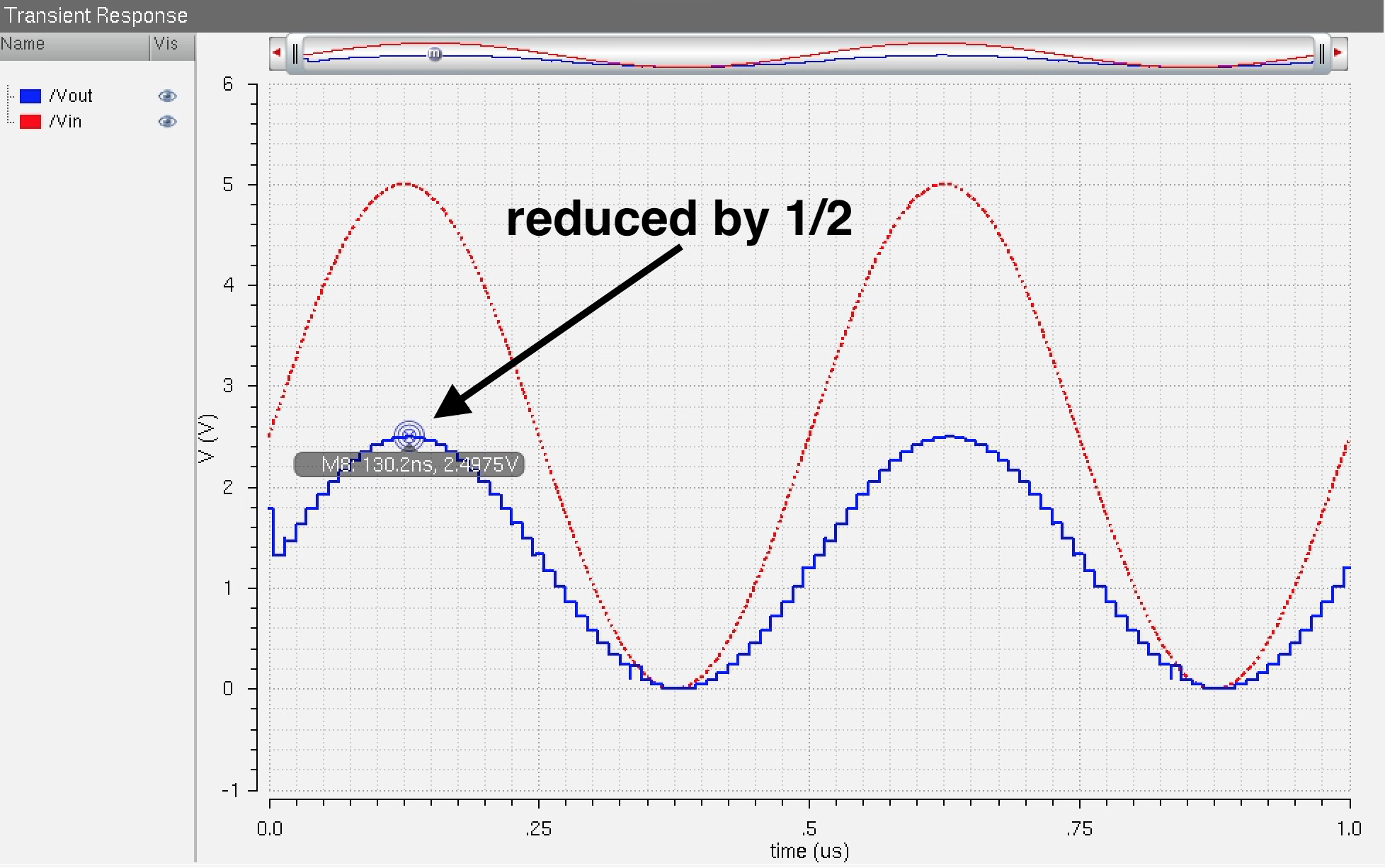
[ 10 ] drive a 10 kΩ load, the output is effectivley half the no-load condition
this occurs because the resistor acts as a voltage divider
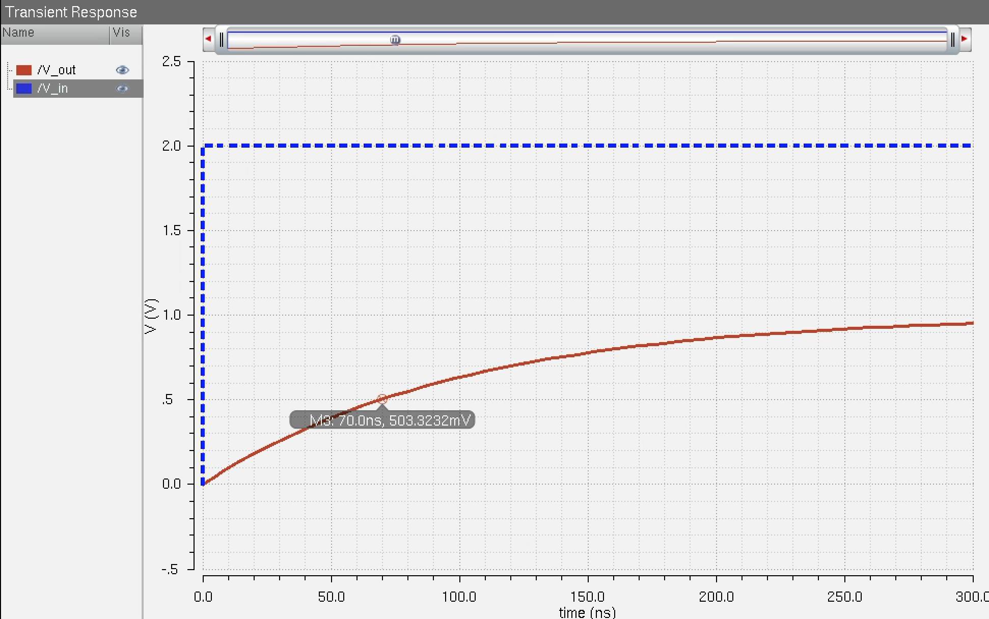
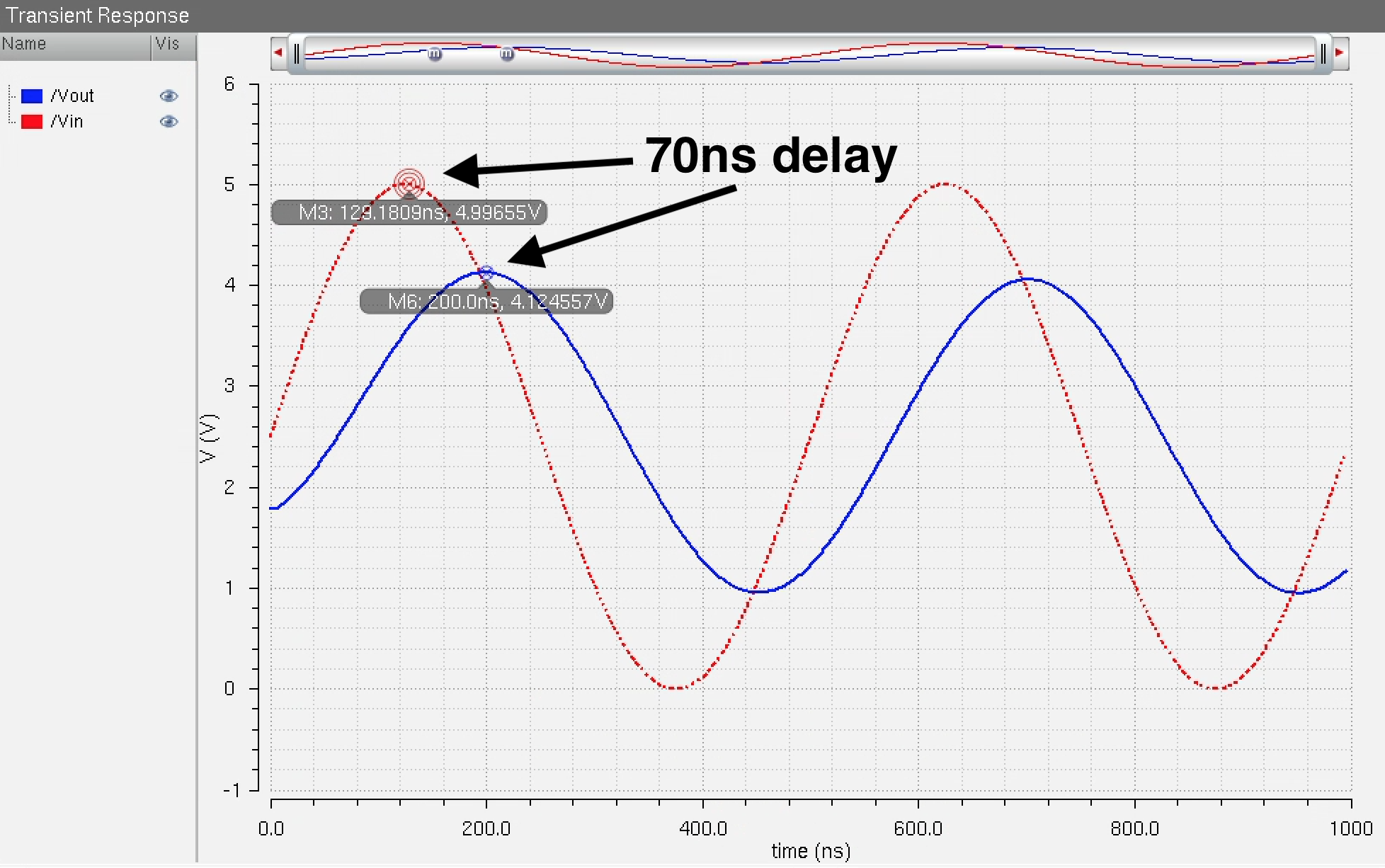
[ 11 ] drive the purely capacitive load C = 10 pF, reduction and delay
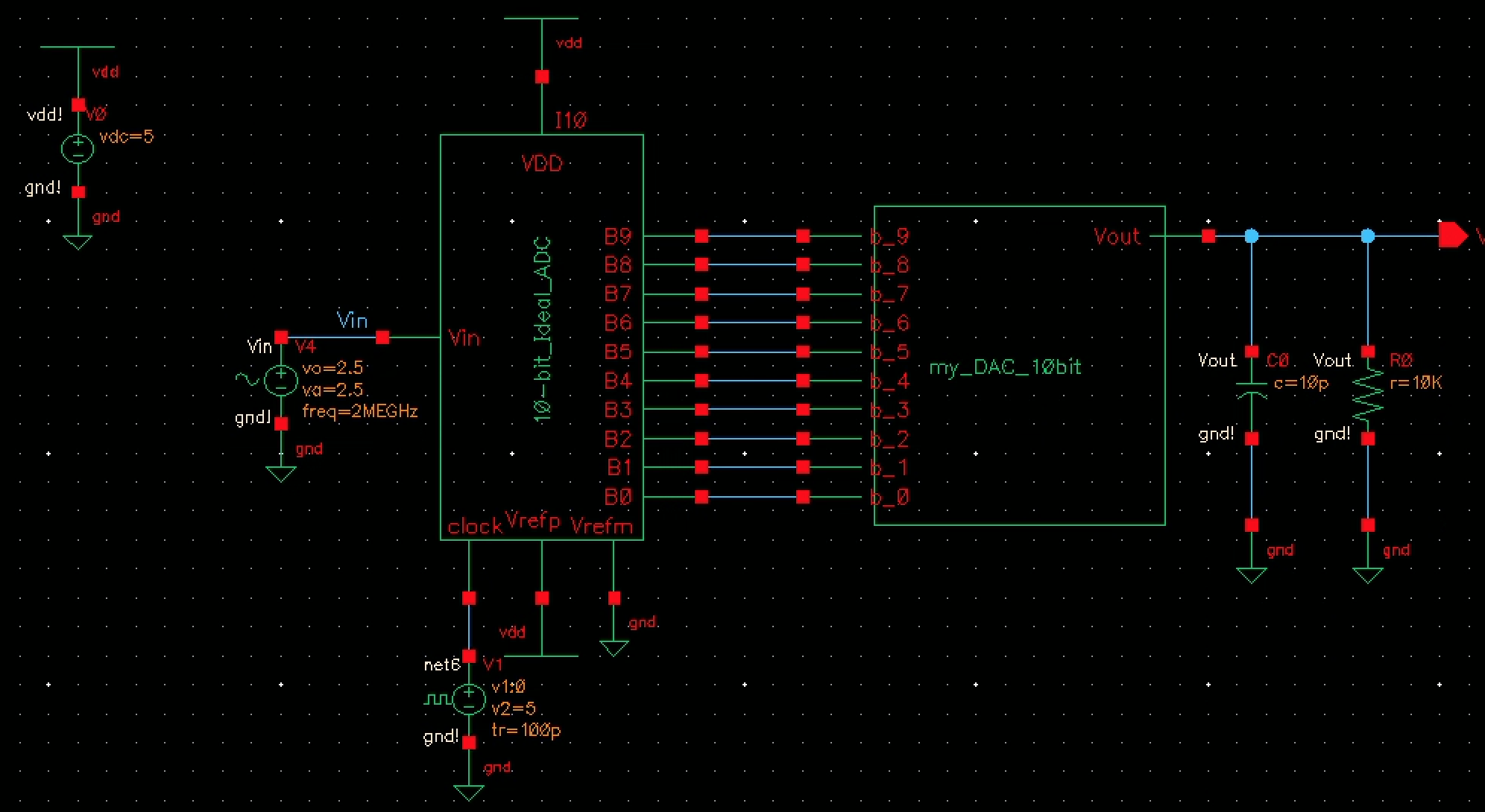
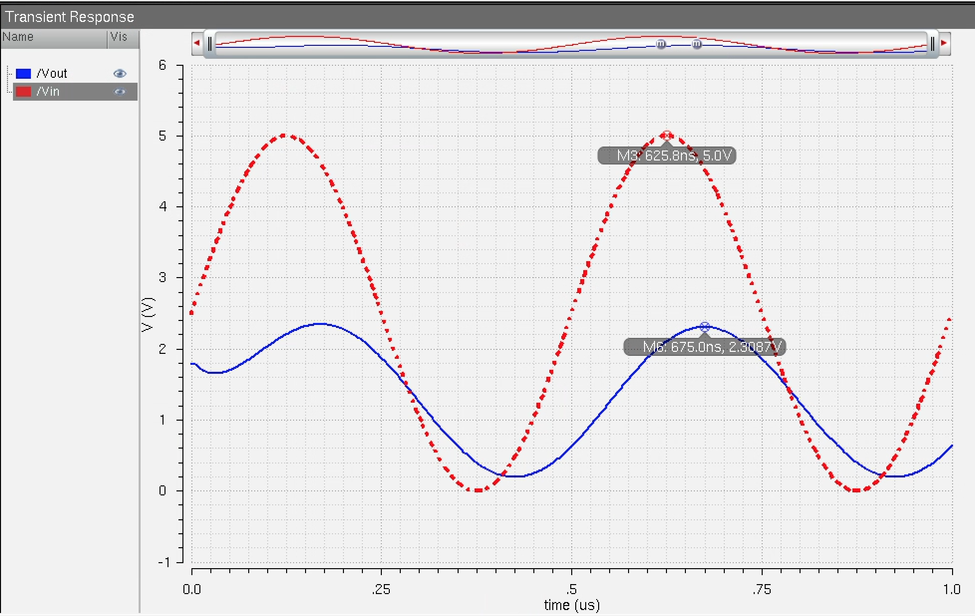
[ 12 ] drive a capacitive and resistive load (a super-position of the R and C individually)
RC time
constant is reduced by resistors in parallel { about 50 ns lag}
[ 13 ] conclusions
MOSFETs tend to have low resistance. In the eveny the
resistance is too high, performance will degrade. Also, a capacitive
load will smooth the output voltage, potentially losing the benift of
the DAC. A purely resistive load reduces output voltage by introducing
the effect of a voltage divider. If the MOSFETs have significant
resistance, these simulations and designs should be adjusted. In
addition, inductance should be considered for some of the components
used to implement the circuit. Total impedance is a very important
consideration for these devices.
