Project – EE-421L
Authored by
Matthew Daniel McDonagh
EE-421 Fall
2021
email: mcdonm6@unlv.nevada.edu
Lab description: This is a design of a register
file (RF) that uses an 8-bit word and has 32 words. The RF uses a 5-bit address
schematic to access the 32 8-bit words. The memory in this project is not
addressable by bits. The remaining inputs to the register file include the 8-I/O
lines for reading and writing, as well as a control signal, RW (LW), for
indicating either a read or write to the RF, and lastly VDD/Ground.
To begin with we utilize a row
driver (an electronic amplifier circuit designed for driving a load), a sensitivity
analysis tool (a method used to identify how much variations in the input
values for a given variable will impact the results), battery pre-charging
(charging at a low rate usually 1/10 the regular rate where the
charger regulates the battery voltage entering the CV phase while the charge
current exponentially drops to a defined termination level), and some bit
comparators (X number of inputs each for X single bit numbers and three outputs
to generate less than, equal to, and greater than between two binary numbers). This
particular design does not include the pre-charger and the sensitivity analyzer
at this stage.
One of the current predicaments
in the industry for memory development are power dissipation and area covered.
The rate at which memory design has increasing advances with scaling in logic
must be met by an equivalent scaling in density. Breaking the overall design
down into seven parts, I will begin with the inverters:
Design:
Inverter
I will start this design with a
basic SRAM (static random access memory) cell and
schematic. The cell of the SRAM will have several tiny transistors, allowing
the cell to flip without difficulty, as well as inverters. Pictured below is
the inverter I will be using:
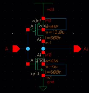
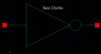
Next is the symbol for the
inverter, size 12u/6u:
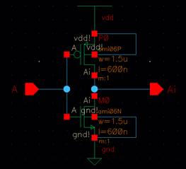
In addition, here is a smaller
inverter for use in the larger components:
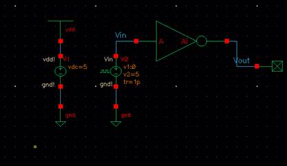
Below is a testing schematic
for simulation purposes (input pin A and output pin Ai notated):
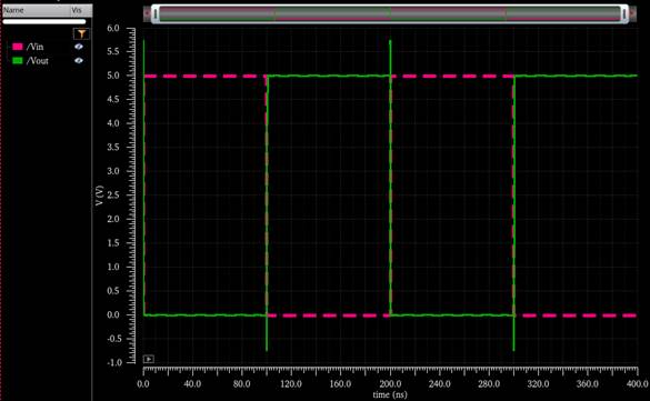
Simulation results
(alternating):
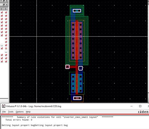
Testing the inverter circuit
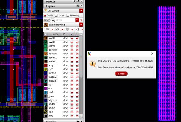
for DRC and LVS pass:
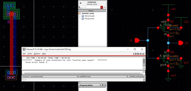
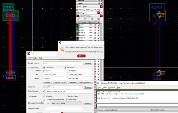
Both DRC and LVS are good. Now
checking DRC and LVS for the smaller inverter:
Design: 1-bit
Cells (for SRAM)
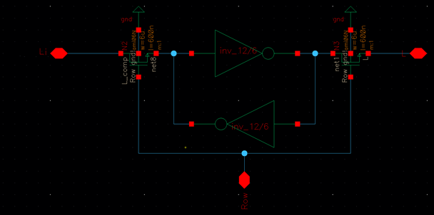
Below is the schematic for the single
bit cell used by NMOS gates which are scaled to not overpower a latch (not DFF).
The line of data (A or D or L) and its complement (Ai or Di or Li) are
critically important to the SRAM. Either L or Li will pass through the NMOS
gate and update the SRAM.
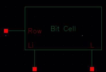
Next is the symbol for the bit
cell:
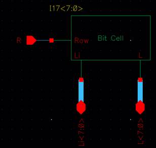
Here is an example circuit for
simulation and testing purposes:
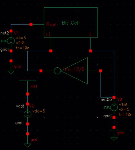
Simulation results:
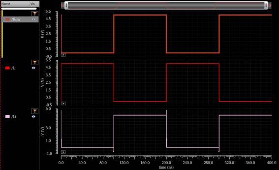
From the simulation we can see
that when the row line is high, the value of L is written to the memory line.
When the row line is low, it ignores the current value of L and remains using
the last known value written.
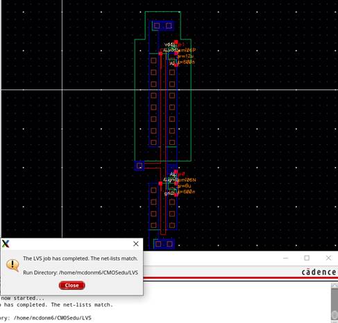
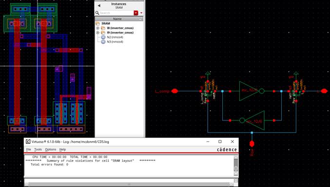
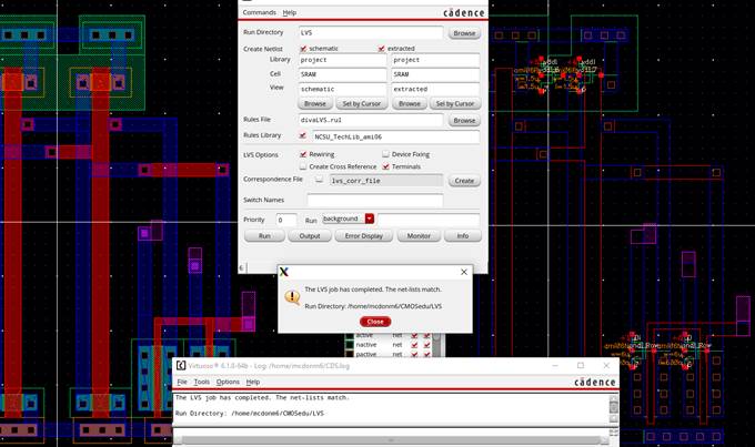
The layout of the SRAM bit cell
is comprised of two inverters and configured with beneficial intersections of
various metals, with some transistors on the bottom. Testing the bit cell
circuit for a passing DRC and LVS:
Design: Word
Cells
Next I took the SRAM / Bit Cell
design above and assimilated it into a single schematic consisting of 8
iterations of it. It represents a single row of memory units. Below is the
schematic for the 8-bit word for the Register File:
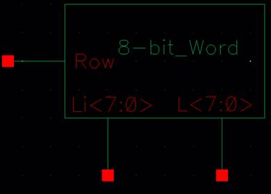
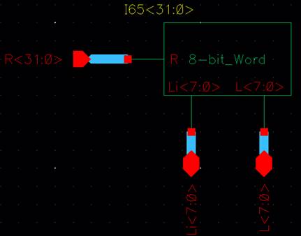
Next is the symbol for the
8-bit word, which consists of 8-bit lines of data, 8-bit lines of complements,
both of which are input into the word cell that determines whether the cells
are activated or not:
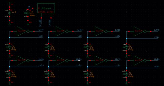
Simulation schematic /
verification circuit for the 8-bit word:
Simulation results:
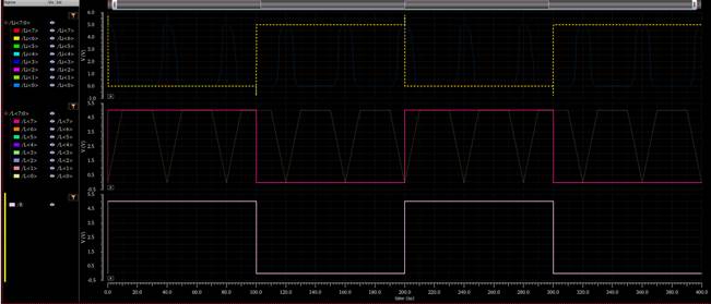
From the simulation results we
can see that when R (row) is high, the SRAM is storing the data value
(L<7:0>) of the cell.
The Layout of the 8-bit Word is
comprised of 8 SRAM cells. Testing the 8-bit Word circuit for a passing DRC and
LVS:
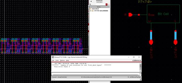
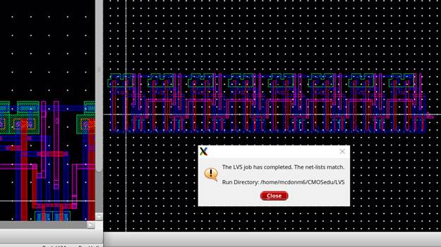
The 8-bit word cell passes both
checks.
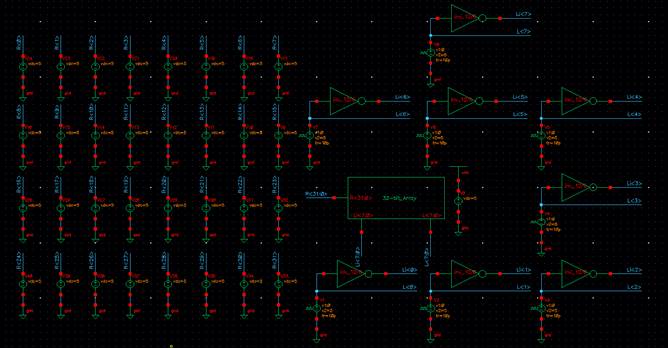
Design: Array
of Words
Next is the array for the 32 word cells, which satisfies the requirement of the design
for a 32x8 word array. It is comprised of 32 different row lines each with a
value determined by L or Li inputs. It also has a decoder that allows the
circuit to mimic the functioning of an SRAM (using 32 row lines). This array
lets us know what word is being accessed, and works similarly to the 8-bit word
cell with the added exception that each row consists of an 8-bit word. For the
schematic below, I replicated the 8-bit word cell for 32 valued iterations:
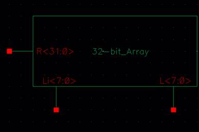
Here is the word array symbol:
Simulation circuit of the
32-bit word array:
Simulation results:
From the simulation results,
the individual bit cell starting at 0 for example, stores a data value when the
row is high.
The layout of the 32-bit word
array contains 32 rows of the 8-bit word layout compiled together with strips
of metal1 connecting the rows. Testing the circuit for a passing DRC and LVS:
The word array successfully
passes all checks. In an industrial setting, a single-bit slice of the 32-word
RF would resemble the following:
Design:
5-input AND Gate
Before constructing the row decoder,
a 5-input AND gate must be realized. This is accomplished by using a 5-input
NAND gate and putting the inverter before the output. This allows the gate to
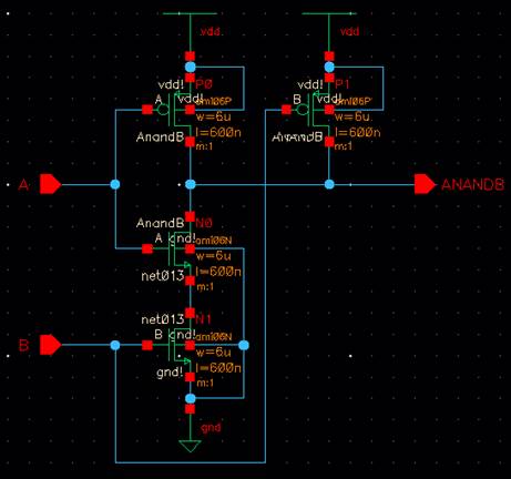
receive the row decoder for future usages. The schematic below is the
preparation of the 5-input NAND gate, starting with a single NAND gate
schematic:
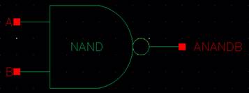
Symbol for a singular NAND
gate:
Next is the singular AND gate
schematic:
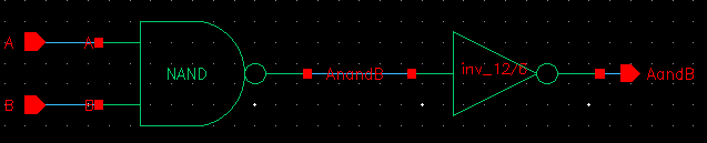
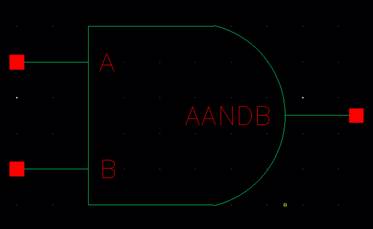
Symbol for a singular AND gate:
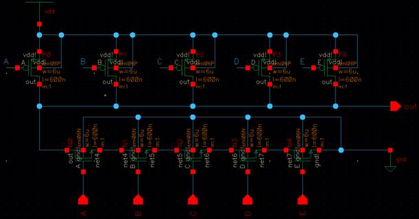
Next is the schematic for the
5-input NAND gate with input values A through E and a singular output:
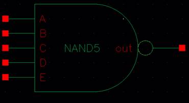
The symbol for the 5-input NAND
gate:
Combining the inverter with the
5-input NAND gate to form the 5-input AND gate:
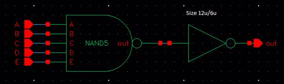
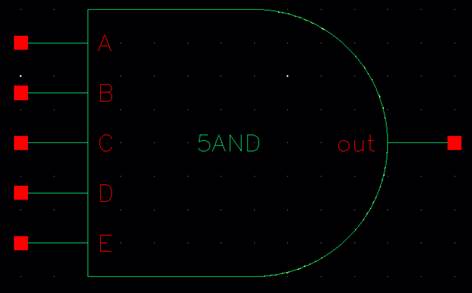
5-input AND gate symbol:
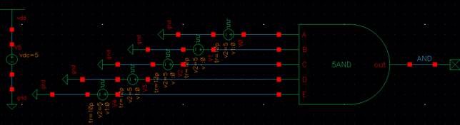
Verification circuit /
simulation schematic for testing purposes:
Simulation results:
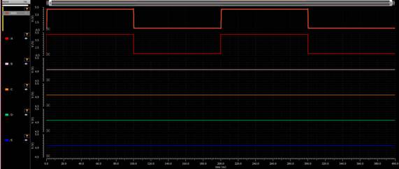
From the simulation results,
when the output (AND gate) is high, the inputs are a 1, and when inputs are a
0, the output is also 0.
The Layout of the 5-input AND
gate contains the layout of the 5-input NAND gate and an inverter. Testing the
5-input AND gate circuit for a passing DRC and LVS:
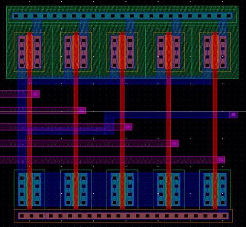
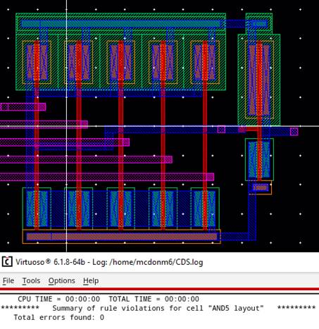
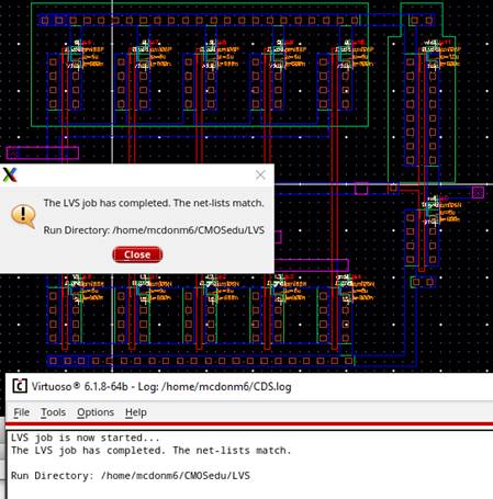
The 5-input AND gate
successfully passes all checks and is ready to implement in the next step.
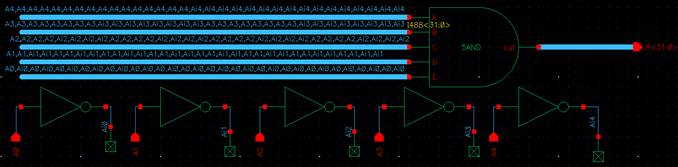
Design: Row
Decoder
The last component to make
before assembling the full register file is the row decoder. Using the 5-input
NAND gate (5-bits), the row decoder will iterate through 32 AND gates, allowing
the decoder to choose from 1 out of 32 rows (0-31) for which 8-bit word cell to
be activated. Each NAND gate will have an inverter placed on its output. Every
5-bit address possibility coincides with one 8-bit word cell (from 00000 to
11111). Below is the schematic for the row decoder:
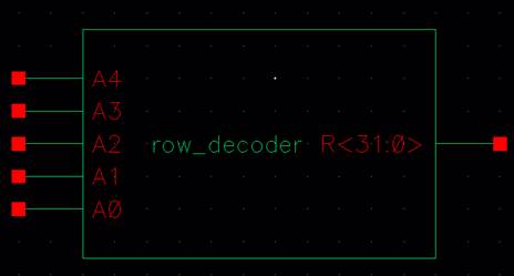
The symbol for the row decoder:
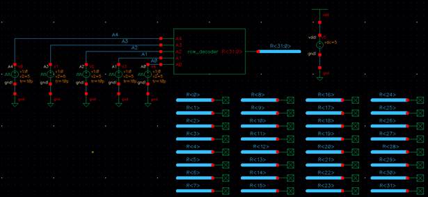
A test schematic used for
simulation purposes:
Simulation results:
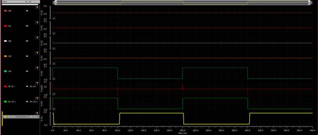
From the simulation results, with
choice of rows 0, 15, and 31 selected, when <A4:A0> are high, row 31 is
on and all other rows are off.
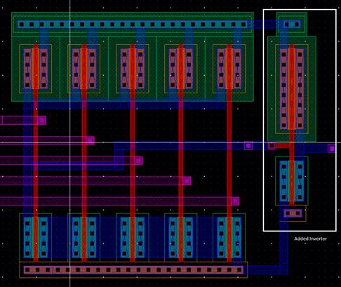
The layout of the row decoder
is comprised of several inverters, and 32 of the 5-input AND gate layouts.
Testing the circuit for a passing DRC and LVS:
Top
of decoder:
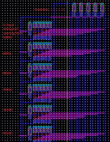
Bottom
of decoder:
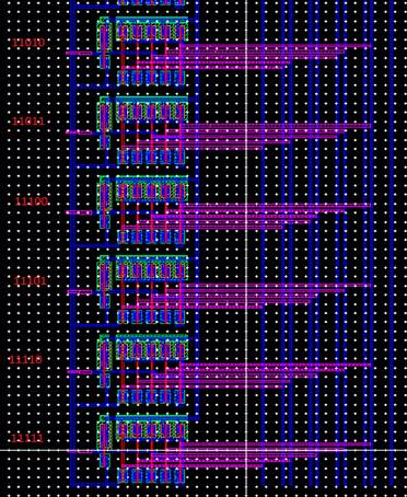
The row decoder passes all
checks, now to implement the final part of the project.
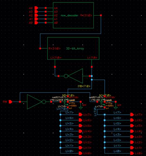
Design: SRAM
Full and Register File
The full SRAM Register File is
constructed by combining the 32-bit word array with the row decoder. The
register accepts an input address for the row decoder to decipher which one of
the 8-bit memory cells must be accessed. Then it will write the value of
L<7:0> into the word cell manually. Below is the schematic for the
Register File:
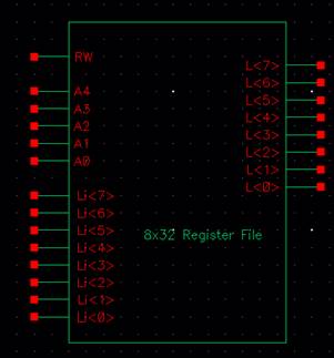
The symbol for the register
file:
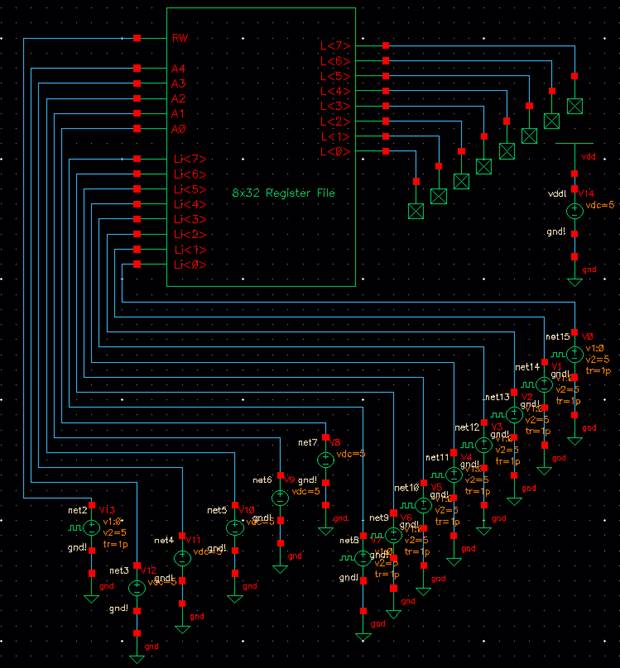
A verification circuit / test
schematic for simulation purposes:
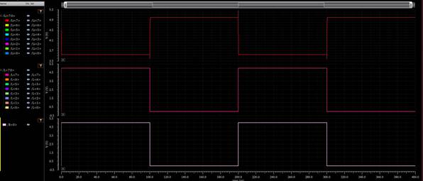
Results of simulation testing:
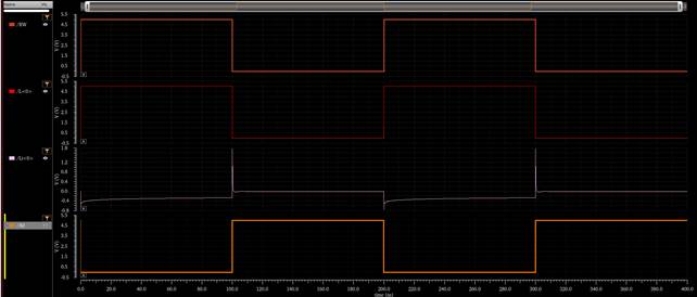
From the simulation results, it
is observed that when RW (top row) changes from high to low, the Register File
output (bottom row) enter write mode. The value of Li<0> will be written
into the address corresponding to the truth table segment “1 1 1 1 1”. When the RW changes from low to high, the Register
File output will switch to read mode, outputting the value in address “1 1 1 1
1” to L<0>.
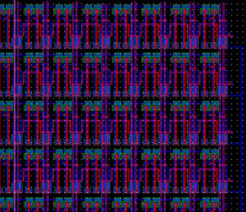
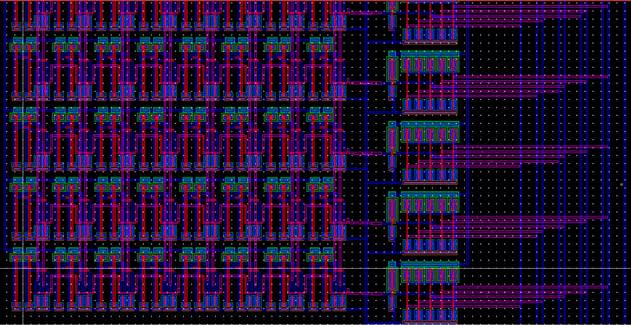
The Layout combines the row
decoder layout and the 32-bit array layout, with added layouts of inverters to
form the final product.
Top
of Register File layout:
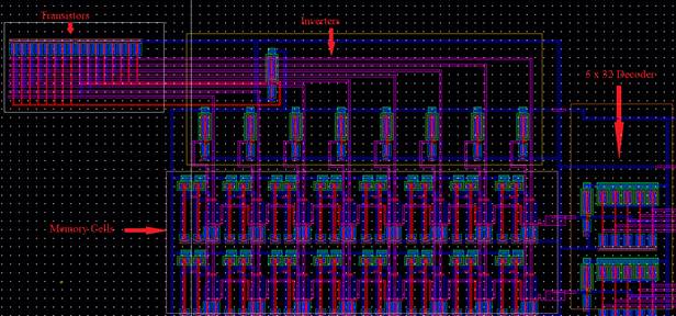
Bottom
of Register File Layout:
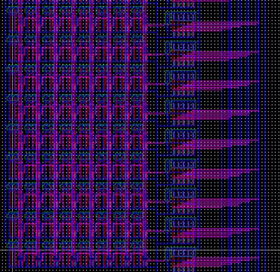
Top
of Register File extracted:
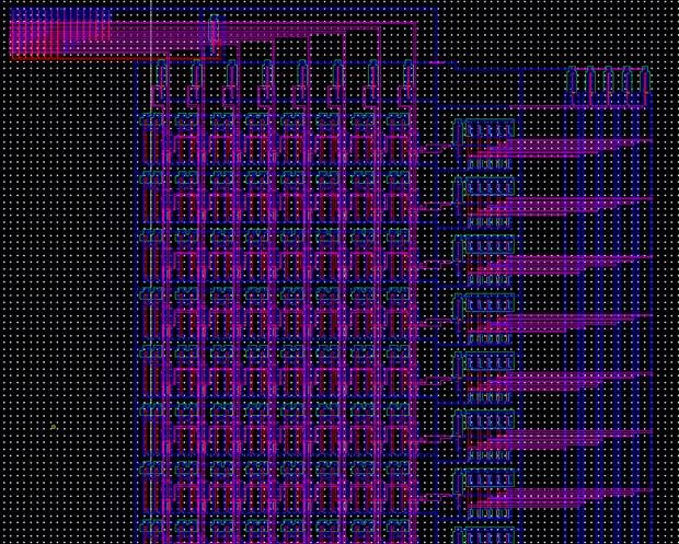
Bottom
of Register File extracted:
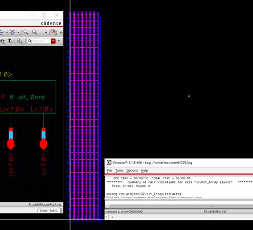
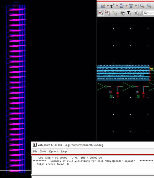
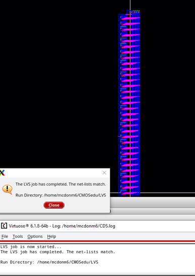
Testing the Register File for a
passing DRC and LVS/netlist check:
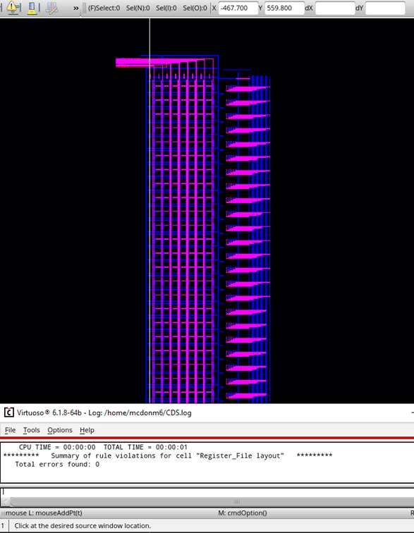
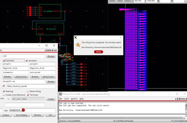
The design passes the checks
and is ready to be implemented into future projects. But this design should be
revamped and refined with finessed schematics before implementing into an
assembly of peripheral components
There are many issues with this
design, but it is my first attempt at something of this magnitude. I am having
trouble reaching maximum output values for L voltages beyond 5 volts. The pre-charger
would probably help in this instance.
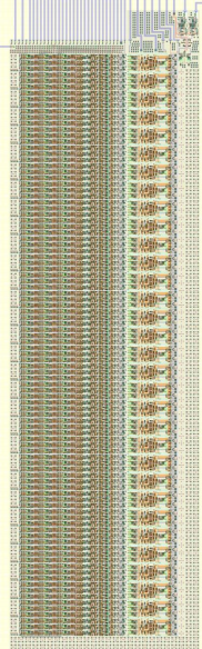
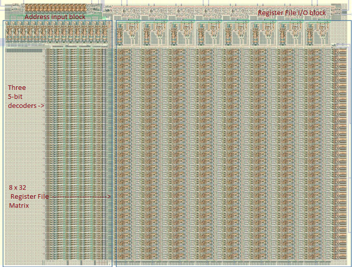
In an industrial setting, the 32x8
Register File would resemble the following:
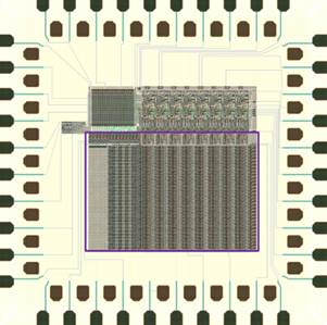
An
example of an 8-bit CPU on a 5x5mm chip would look like this: