Lab 8 –
EE-421L
Authored by Matthew Daniel McDonagh
EE-421 Fall 2021
email: mcdonm6@unlv.nevada.edu
Lab description: Generating a test chip layout for submission to
MOSIS for fabrication. The requirements for this lab’s chip include the
following components:
A. A project for the course
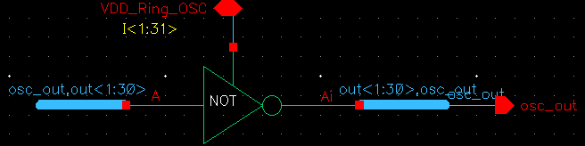
B. A 31-stage ring oscillator with a buffer for driving a 20pF off-chip load
C. NAND gate using 6/0.6 NMOS/PMOS
D. NOR gate using 6/0.6 NMOS/PMOS
E. Inverter made with a 6/0.6 NMOS and 12/0.6 PMOS
F. Transistors both PMOS and NMOS 6u/0.6u with all 4 terminals
connected to bond pads
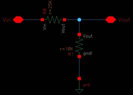
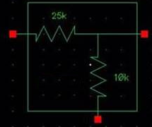
G. 25k Resistor & 10k Resistor implementing a voltage divider
H. 25k Resistor implemented using the n-well connected between 2
pads
Pre-lab work:
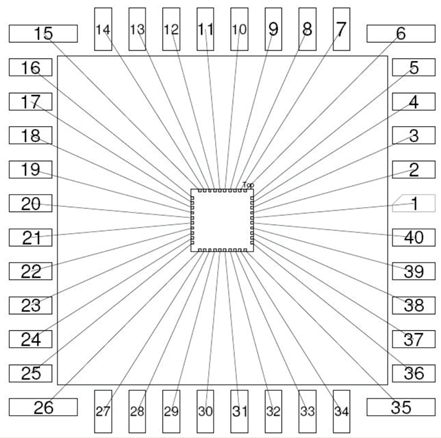
Following along tutorial 6, we first must recognize the pin
arrangement:
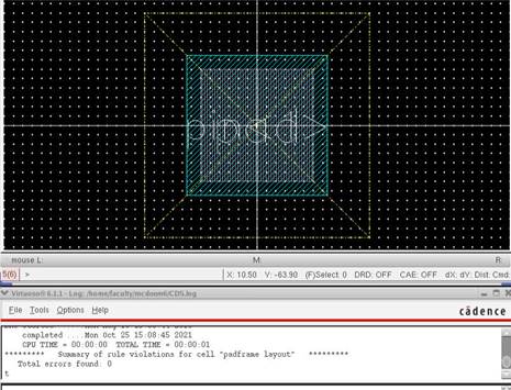
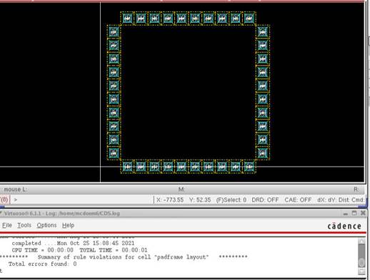
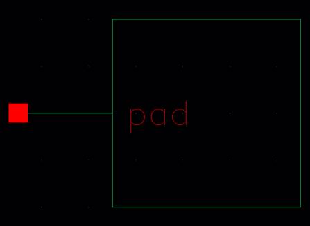
Next is to create a layout of a pad and verify with a DRC check:
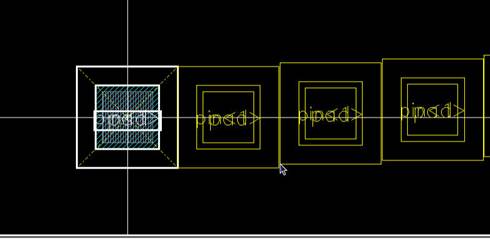
Next copy a 12x12 pin array
Make sure that the pad frame is error-free.
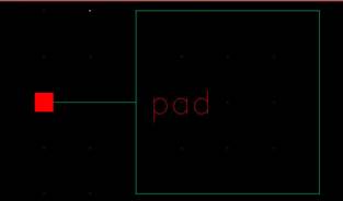
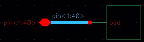
Next we make a schematic for the pad as well as a symbol:

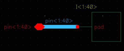
Then use an array to create a schematic of the pad frame symbol:
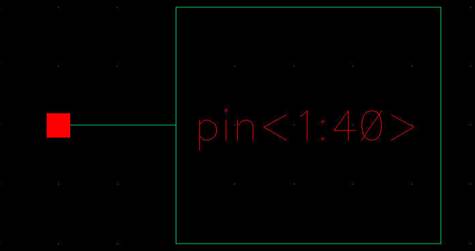
Then use that schematic to make a symbol of the pad frame:
Then make a schematic of the chip:
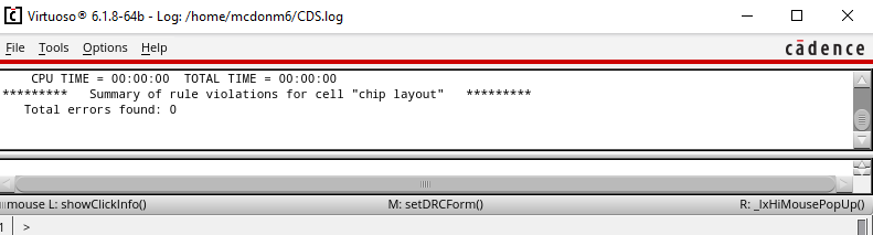
Then place the components in a layout and verify with a DRC check:
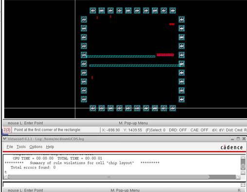
The checks pass, this concludes the pre-lab portion of lab 8.
Next, we move on to the design. Each circuit requires its own
power supply, although the ground pin is the same to them all. This was
explicitly stated in the instructions to reduce the number of pins required
overall by sharing them. Starting with the pad frame:
From tutorial 6, the pad frame is in good functioning condition.
The pad is within MOSIS limits. Here it is broken down, pad schematic and
symbol:

Padframe schematic and symbol:
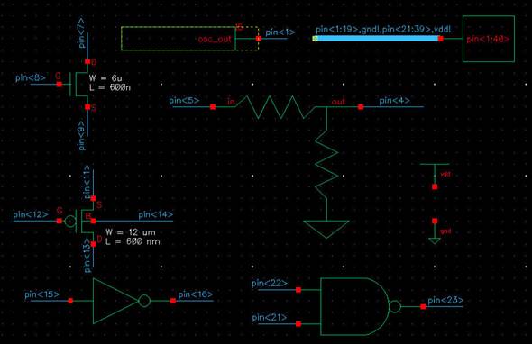
An overall picture of the course project schematic and symbol:
Layout of the course project:
Extracted:
DRC and LVS already confirmed for bonding pad.
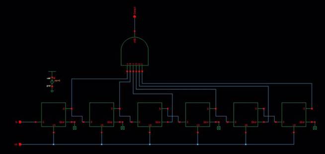
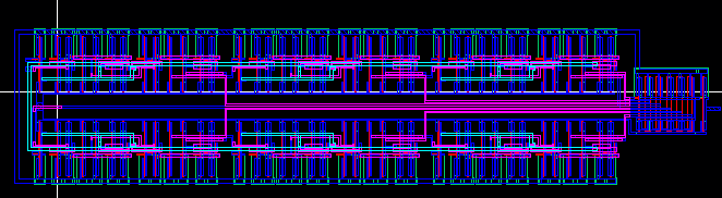
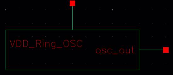
Next is the 31-stage ring oscillator, starting with the schematic
and symbol:
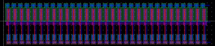
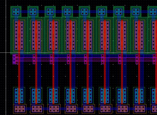
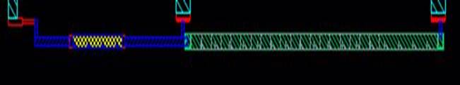
The layout of the ring oscillator:
Zoom of left side:
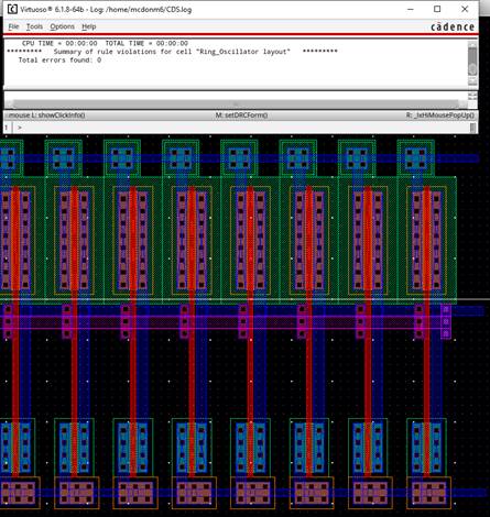
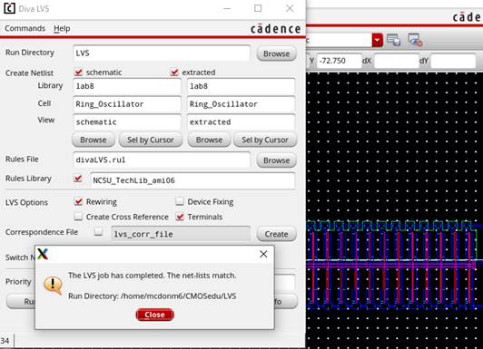
Confirming a DRC and LVS pass for the ring oscillator:
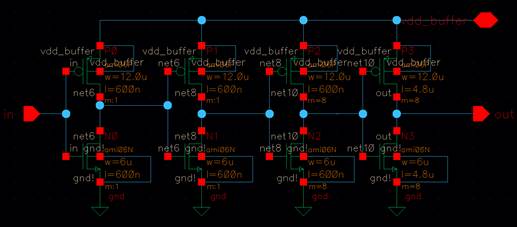
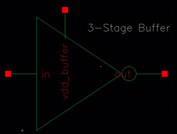
Next is the 3 stage buffer, starting with the schematic and the
symbol:
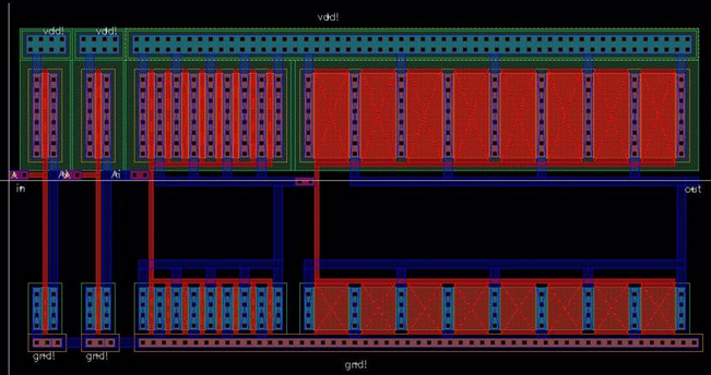
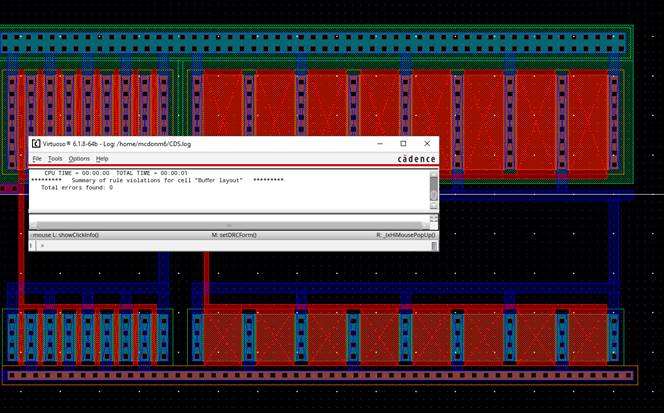
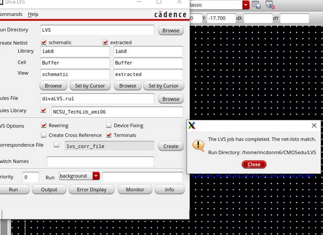
Next is the layout of the buffer and a passing DRC & LVS:
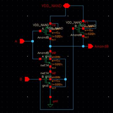
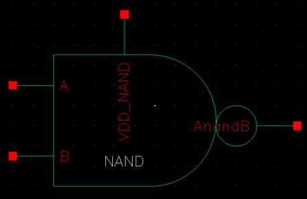
Next is the NAND gate, starting with the schematic and symbol:
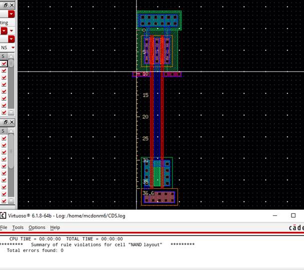
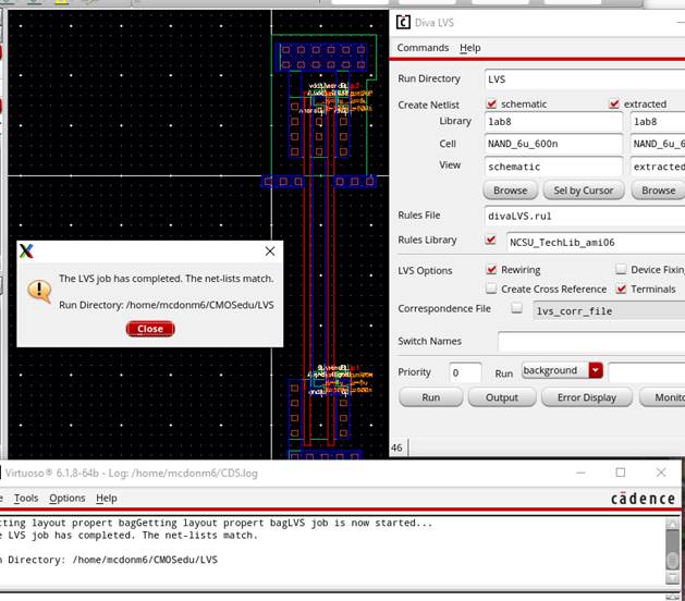
The layout of the NAND gate with a passing DRC and LVS:
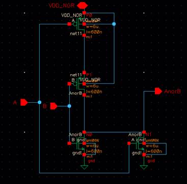
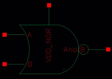
Next is the NOR gate, starting with the schematic and the symbol:
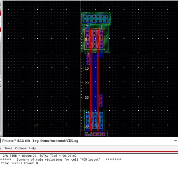
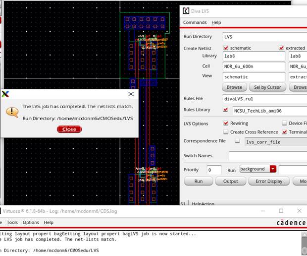
Next is the layout of the NOR gate, with passing DRC and LVS:
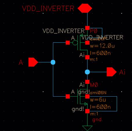
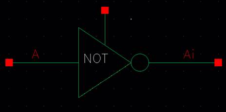
Next is the Inverter, starting with the schematic and the symbol:
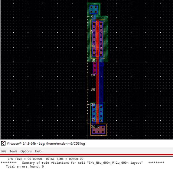
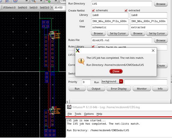
The layout of the inverter, with a passing DRC and LVS:
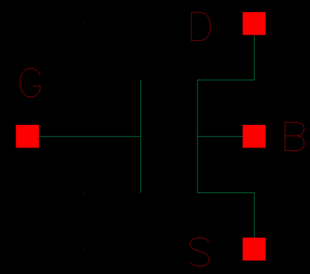
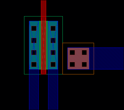
Next, the transistors, starting with NMOS schematic and layout (Body
to ground -> pin 20, D/S -> pin 9 & 11, gate -> pin 10):
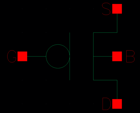
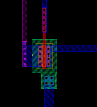
PMOS schematic and layout (VDD -> pin 12, D/S -> pin 12
& 14, gate -> pin 13):
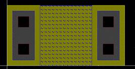
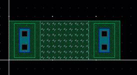
Next is the voltage divider schematic, symbol, and the 25k/10k
resistor layouts implemented:
The completed schematic of the chip with all the required
components therein:

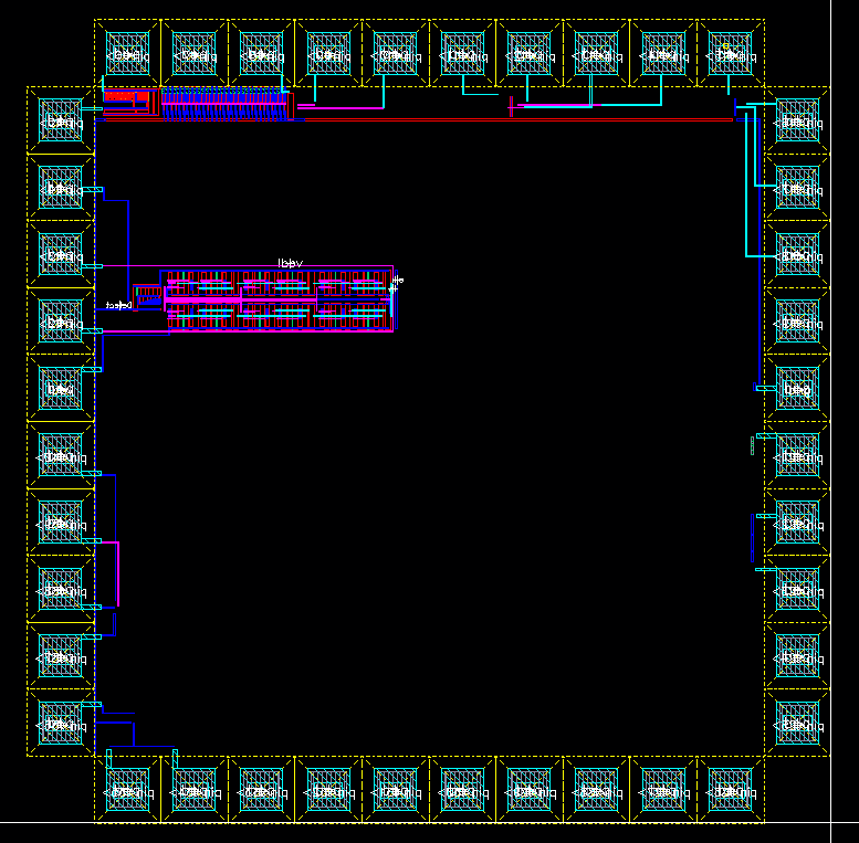
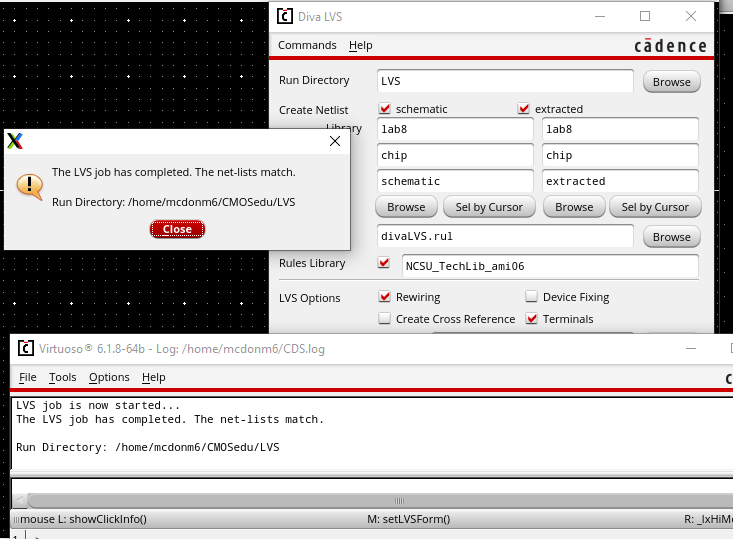
Layout of the completed chip,
with passing DRC and LVS:
This concludes the lab and shows that the chip is working in the
very least for design checks. More components can be created for use of this
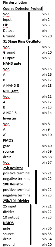
chip for more advanced designs. Below is a pin reference list I used when
setting up the connections.