Lab 7 – EE-421L
Authored by Matthew Daniel McDonagh
EE-421 Fall 2021
email: mcdonm6@unlv.nevada.edu
Lab description: In this lab we will be using buses and arrays in
the design of word inverters, muxes, and high-speed
adders. The purpose of this lab is to demonstrate the usage of buses to simply
drive multiple components. Beginning from simple MOSFETs to CMOS to gate-level
design components, this lab will reinforce the expansion of our own skills to
navigate more complicated circuits. We utilize wide wires (shift-w) for easier
visual reference.
Pre-lab work:
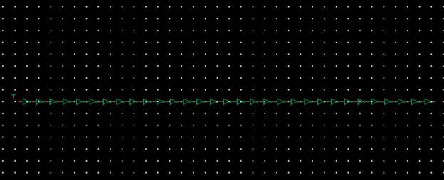
Beginning with Tutorial 5, we start with creating a schematic and
a model for a ring oscillator:
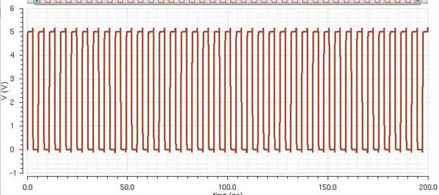
Simulation of Ring Oscillator:
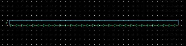
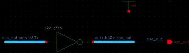
The layout of the ring oscillator:
This concludes the pre-lab portion of lab 7, next is the first
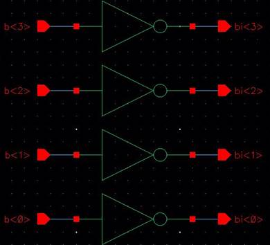
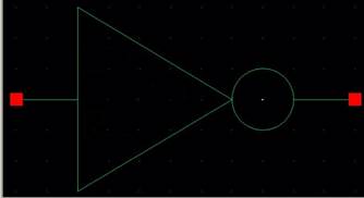
experiment, examining the circuit used for inverting a 4-bit word, symbol of
which is seen below:
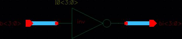
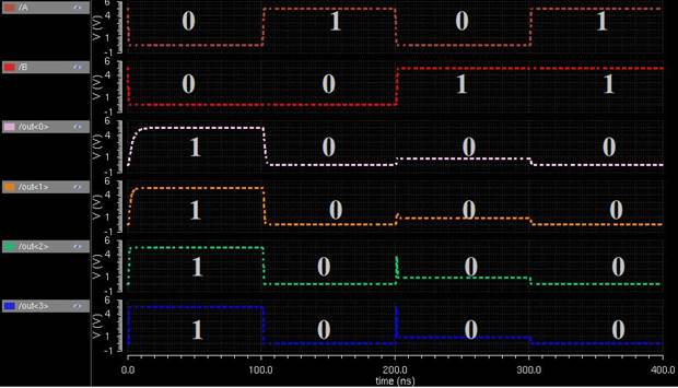
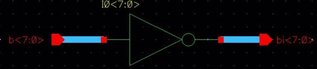
Here is a schematic of the inverter:
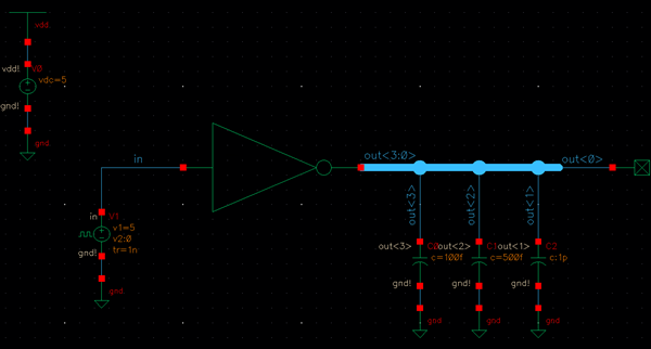
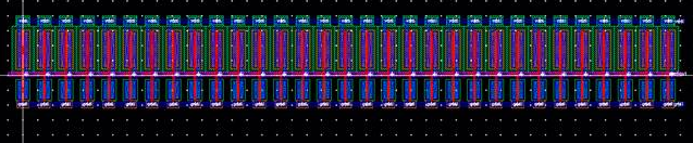
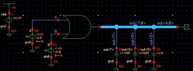
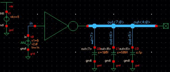
Below are the results of the simulation, showing 4 separate
running inverters with different capacitance loads:
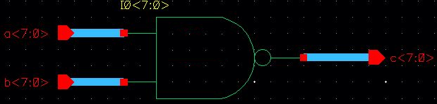
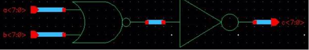
Next we must create schematics and
symbols for 8-bit input/output arrays of NAND, NOR, AND< OR, and inverter
gates:
First is the NAND gate, starting with the symbol:
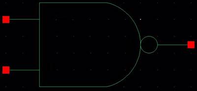
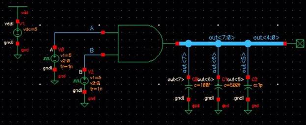
The NAND gate schematic:
Updated NAND gate schematic for simulation:
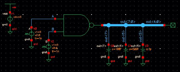
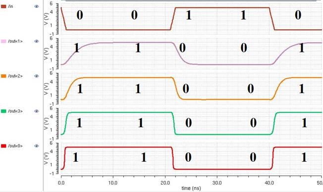
NAND gate transient simulation response:
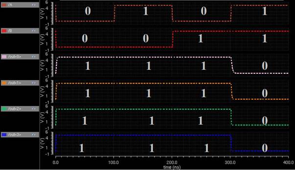
NAND gate simulation complies with NAND gate truth table:
A B | Y
0 0
| 1
0 1
| 1
1 0
| 1
1 1
| 0
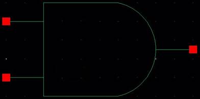
Next is the AND gate, starting with the symbol:
AND gate schematic:
Updated schematic for simulation:
AND gate transient response simulation:
AND gate simulation complies with AND gate truth table:
A B | Y
0 0
| 0
0 1
| 0
1 0
| 0
1 1
| 1
Next is the OR gate, starting with symbol:
The OR gate schematic:
Updated OR gate schematic for simulation:
OR gate transient simulation response:
OR gate simulation complies with OR gate truth table:
A B | Y
0 0
| 0
0 1
| 1
1 0
| 1
1 1
| 1
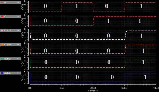
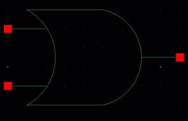
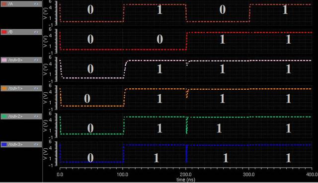
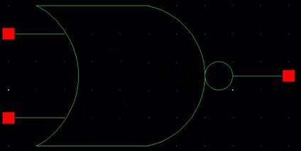
Next is the NOR gate, starting with the symbol:
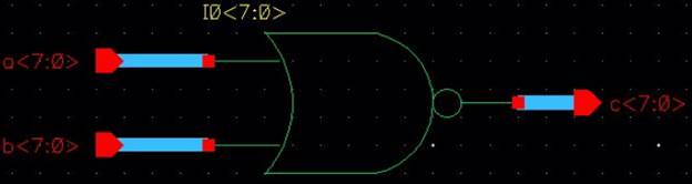
The NOR gate schematic:
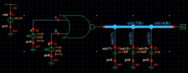
NOR gate updated schematic for simulation purposes:
NOR gate transient simulation response:
NOR gate simulation complies with truth table of NOR gate:
A B | Y
0 0
| 1
0 1
| 0
1 0
| 0
1 1
| 0
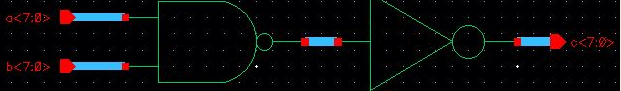
Next is the inverter (not gate) starting with the symbol:
Inverter schematic:
Updated inverter schematic for simulation purposes:
Inverter transient response simulation:
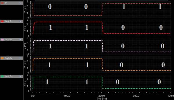
Simulation of inverter (not) complies with truth table for
inverter:
A | Y
0 |
1
1 |
0
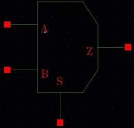
Next is to examine the schematic file of the 2-1 DEMUX/MUX and its
symbol and simulate the operation of the circuit. The lab gives us the
schematic, which I have opened up and edited slightly.
There are four inputs, A B S and Si, the latter two are used to switch-off
between various inputs the user can decide on. In the mux these
two control which outputs a singular input connects to, and in the demux these two will decide if A or B are utilized for an
input for a specified output. The multiplexer operates by choosing A when input
S is high and choosing B when input S is low, and also
passing the signal of the selected input. The demux
is a decoder that reverses the mux. Below is the symbol:
Schematic of the mux/demux, removed an
input by adding an inverter:
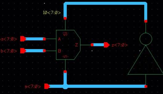
Updated schematic of the mux/demux for
simulation and multiplexer testing:
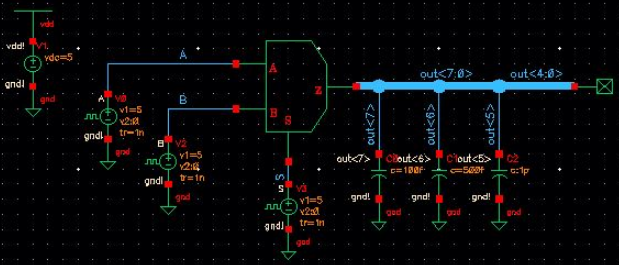
Mux/Demux transient simulation response
from the circuit above:
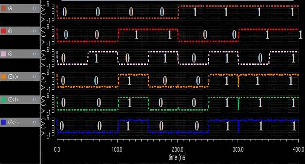
Testing the demultiplexing operation, going in the opposite of
multiplexing means that while S is high the A input is equivalent to Z and when
S is low the B input is equivalent to Z:
Next is the full adder seen in Fig 12.20 using 6u/0.6u devices,
the 8-bit adder is different than the 2-bit adder in that its layout does not always
make use of buses and must be wired approximately, which can be done by
creating an input pin for every A input (from 7:0) and B input (from 7:0) as
well as a singular Cin and Cout
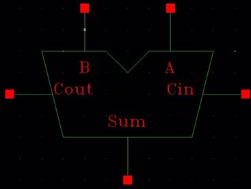
pin. Starting with creating a symbol for the adder:
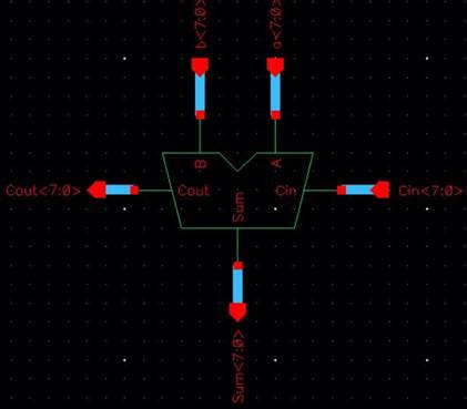
Schematic for the 8-bit Adder
(schematic can use buses unlike layout):
Updated 8-bit schematic for the Adder
for simulations:
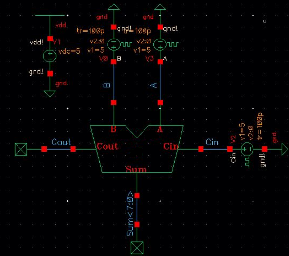
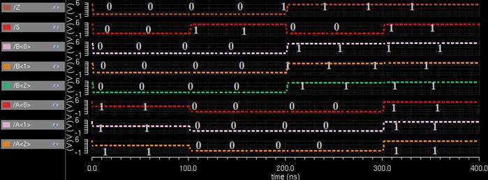
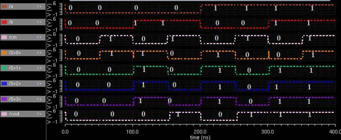
Transient simulation response for
8-bit Adder:
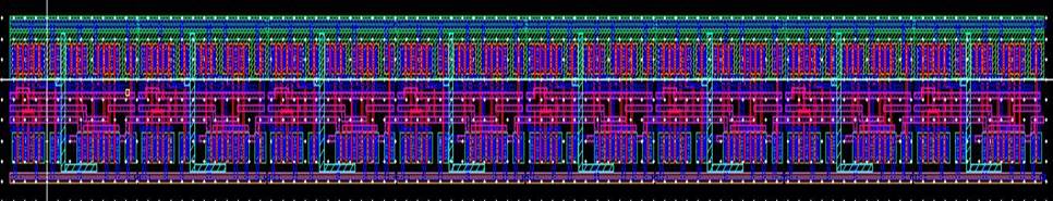
Layout for the full adder,
chained together because no buses were used, retitling each A, B, and Sum pin
from 0 to 7:
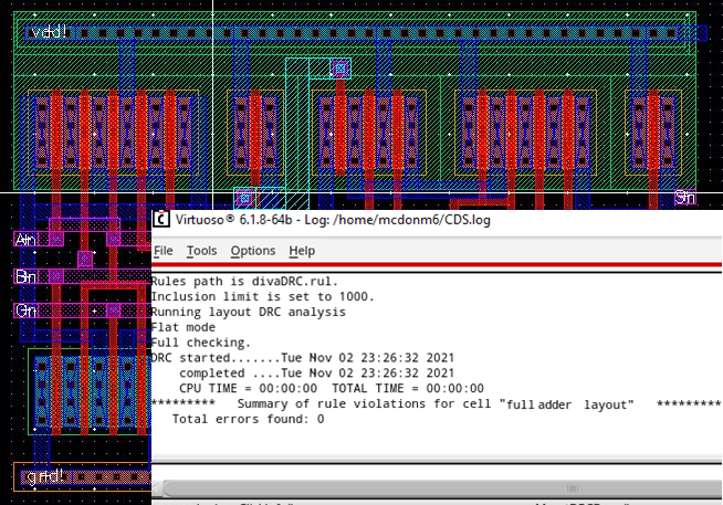
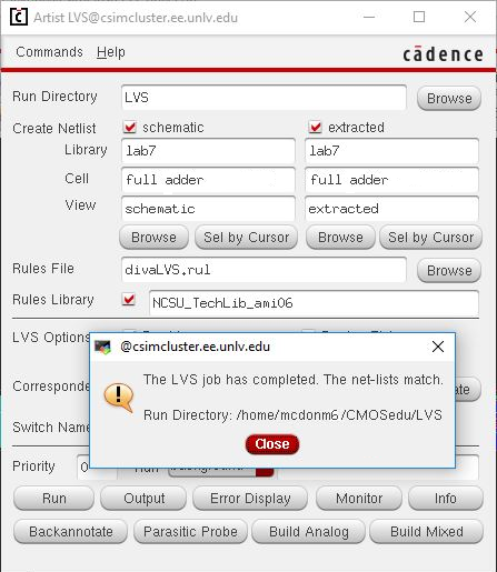
Confirming the DRC and LVS of the
layout:
Conclusion: per lab instruction only
the layout is required for this exercise.