Matthew Daniel McDonagh NSHE:2001509804
email: mcdonm6@unlv.nevada.edu
Lab 6 – EE-421 Fall 2021
Lab
Topic: Design, Layout, and Simulation of a CMOS NAND gate, XOR gate, and
Full-Adder
Pre-lab work: ensure all work is backed up, begin
Cadence Tutorial 4.
The first part of tutorial 4 covers the building of a
NAND gate, as seen here when done:
Next
we make the symbol for the NAND gate, as seen here:
Then we create the circuit schematic for simulation
purposes:
Testing out a simulation of the NAND gate schematic:
The simulation is a proper NAND gate.
The next part is to create the layout, to check the
DRC of the NAND gate (involving copy/paste, dragging, pin creation,
straightening bottom of and removing metal1 / contacts in NMOS):
The DRC is confirmed. Next is to check the extracted
view and confirm the LVS test:
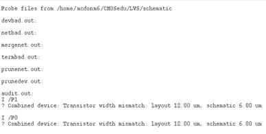
The netlists match, but it should be noted that the
size of the PMOS in layout is not the same as the device in the schematic,
enabling FET params comparison shows this:
This completes the tutorial portion and prelab section.
Now we draft the schematics and layouts for a 2-input
NAND gate and a 2-input XOR gate using 6u/0.6u MOSFETs. Afterwards we are to create
a symbol for both and verify functionality. At the end we will construct a
Full-Adder using these NAND and XOR gates consisting of both a layout and a
schematic, ensuring DRC/LVS success.
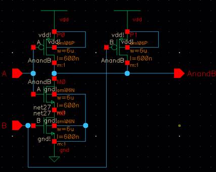
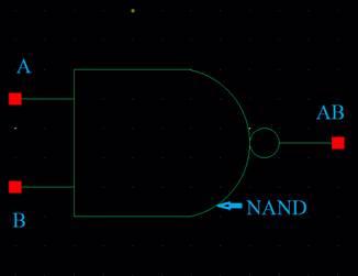
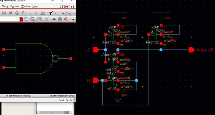
Here is the schematic and symbol for the 2-input NAND
gate:
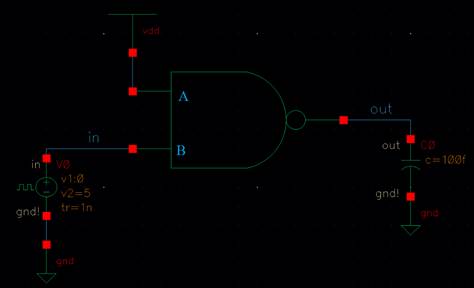
Test schematic for simulation purposes:
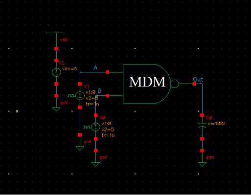
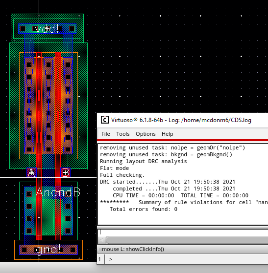
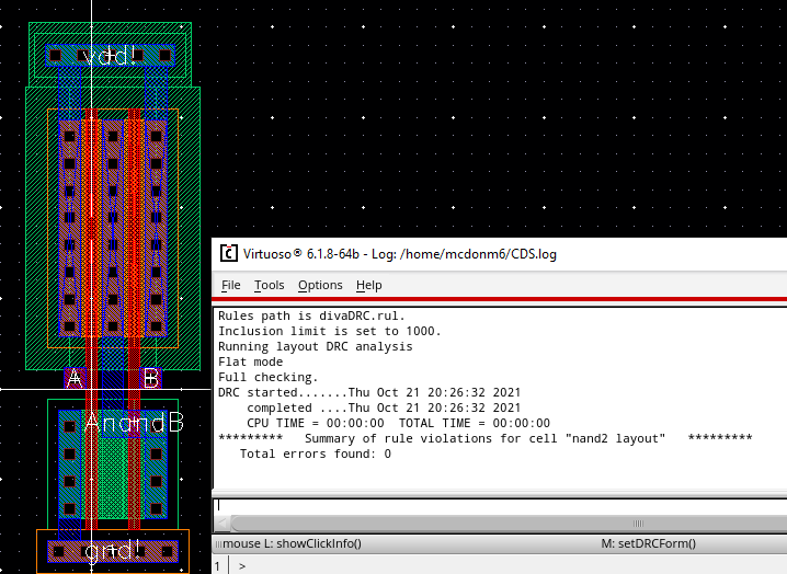
Confirming DRC passes check from the lab6 2-input NAND
gate layout:
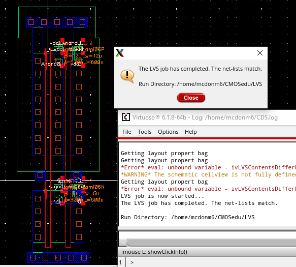
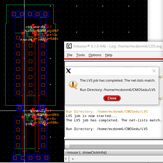
Confirming LVS passes check from the extraction view
of the lab6 layout:
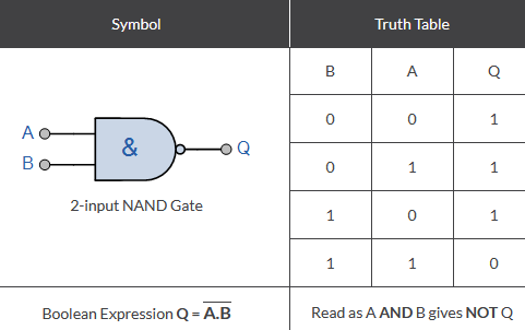
Truth table for a 2-input NAND gate:
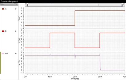
Simulations of the 2-input NAND gate (with inverters
added on to test circuit):
Simulation matches the truth table above, confirms consistency.
Now here is the schematic and symbol for the 2-input
XOR-gate finishing from earlier:
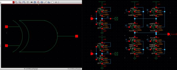
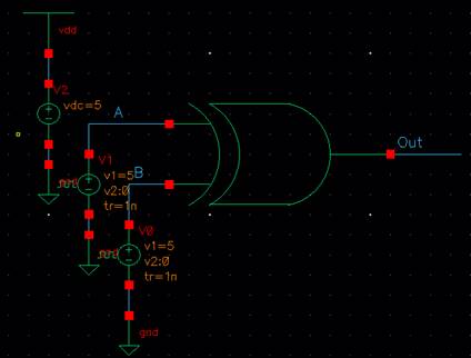
Testing circuit for simulating the 2-input XOR gate:
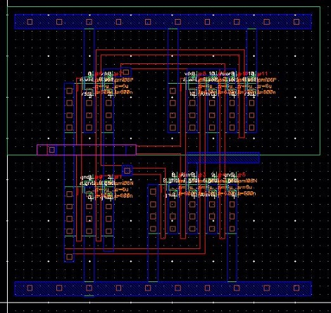
Layout for the 2-input XOR gate, and corresponding DRC
check:
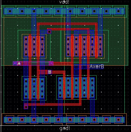
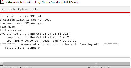
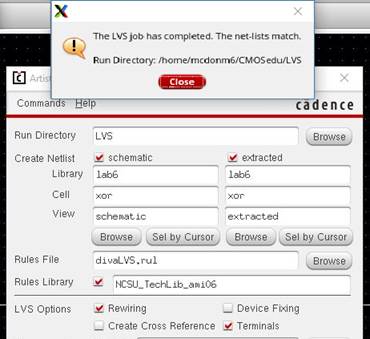
Extracted view with a verification of the passing DRC:
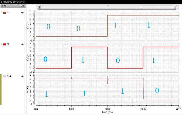
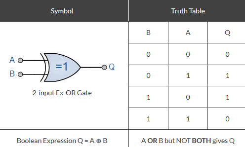
Truth table for a 2-input XOR gate:
Simulation of the 2-input XOR-gate:
Simulation matches truth table of the XOR gate, so
results are consistent.
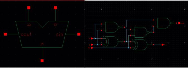
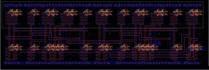
Now we make the Full-Adder, starting with its
schematic and symbol views:
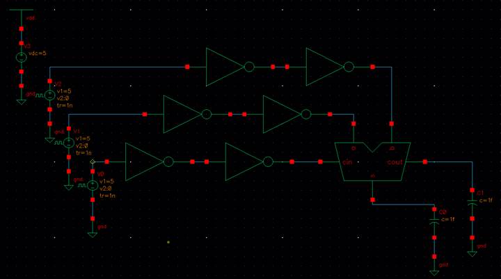
Example circuit for simulation purposes of the full
adder:
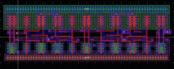
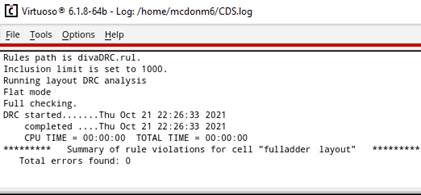
Now after constructing the layout view, check for DRC
verification:
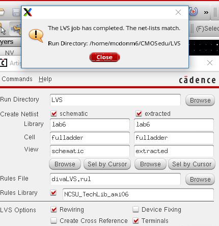
Then confirming the extracted layout view passes the
LVS test:
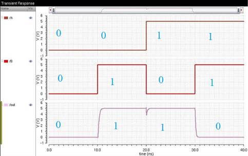
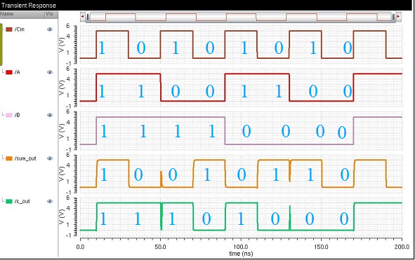
Truth table of the Full Adder:
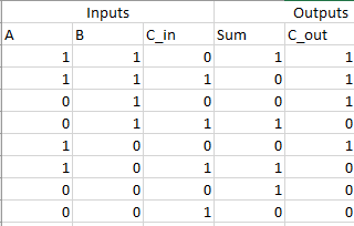
A Simulation of the full-adder circuit matching up
with the truth table of both the 2-input NAND gate and the 2-input XOR gate,
results verify consistency.
Conclusion: these simulations prove the NAND gate, XOR
gate, and Full-Adder are working as designed.