Lab 5: Design, Layour, and Simulation of CMOS
Inverter
EE 421L Fall 2021 – Digitial IC Design
Student name: Matthew D. McDonagh
Email: mcdonm6@unlv.nevada.edu
Lab description: The combination of NMOS and PMOS MOSFET allows for many
applications. This lab in particular exposes the students to basic designs,
layouts, and simulations of CMOS inverter. There are many types of applications
beyond this lab that also rely on this principle. Completion of the tutorial
will develop the skills needed to finish this lab. This lab is broken up into
two major tasks: first, complete and document the library Tutorial_3, then
design, layout and simulate the schematic.
Part 1 (prelab) Tutorial 3:
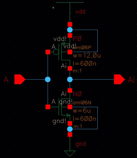
For this prelab, following along with the tutorial_3 shows us how to
design, layout, and simulate a CMOS inverter, beginning with creating a library
named Tutorial_3, then the new cell for the schematic of the inverter.
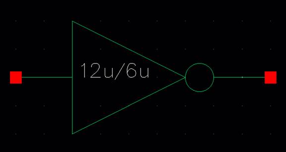
The pins are labeled A for input / Ai for output, then the symbol for the
12u/6u inverter:
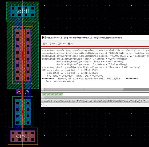
Next is the layout, and extraction.
Confirming the Design-Rule-Check validates with no errors:
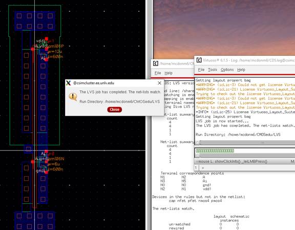
Confirming the Layout Versus Schematic matches:

Created the simulation schematic including the inverter symbol:
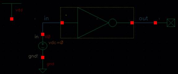
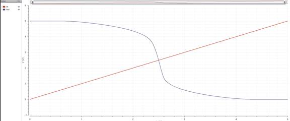
Simulation of the operation of the inverter with Vdd
enabled:
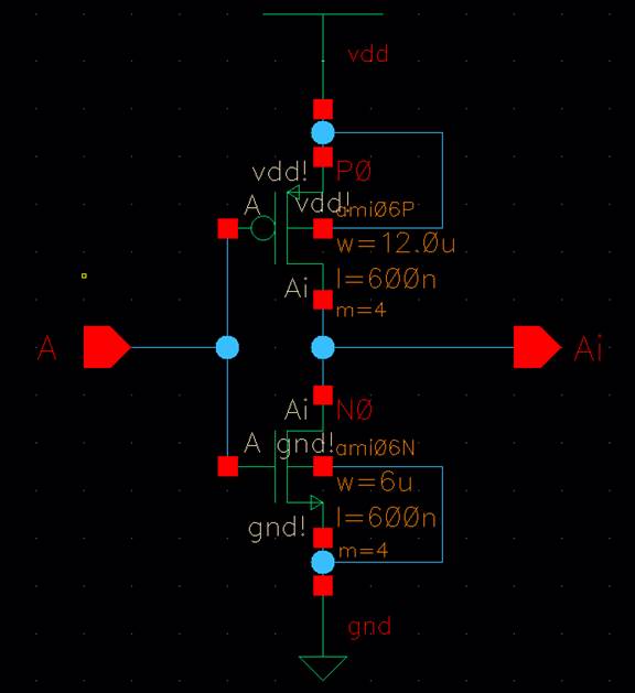
Part 2: Lab 5 standard CMOS Schematic of the first inverter of 12u/6u. Here is the 4-terminal standard cell size
schematic:
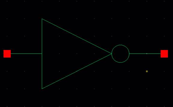
Next is the standard CMOS symbol for the inverter in this case:
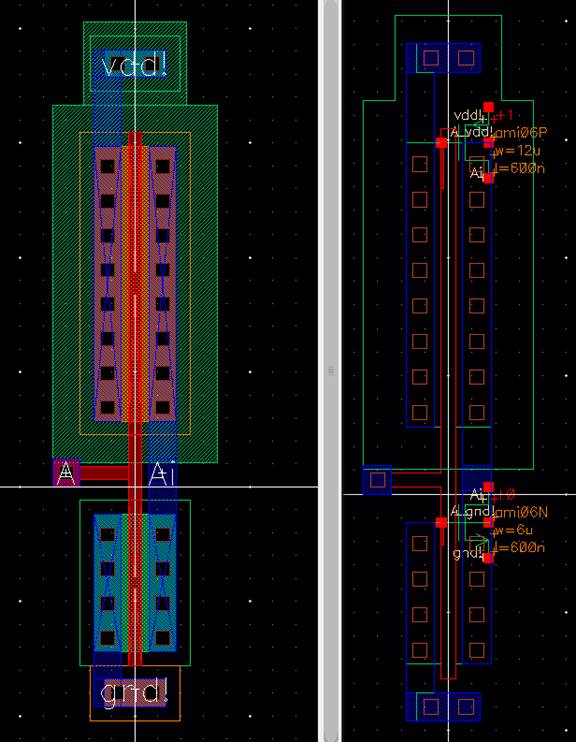
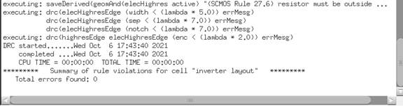
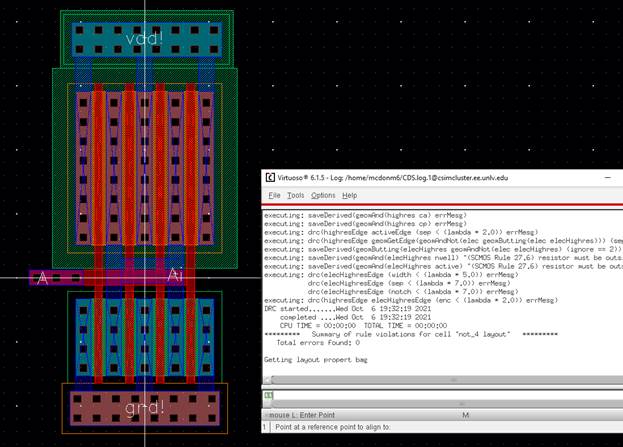
Next will DRC the standard CMOS Layout, verifying no errors:
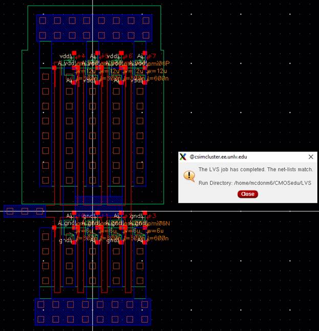
Next will LVS the extracted CMOS layout, confirming the net-lists match:
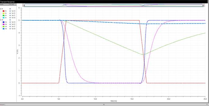
Now the graphed simulations of the 12u/6u inverter with VDD from 0-5V and
varying levels of capacitance:
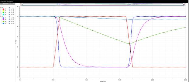
The UltraSim graphs for the inverter:
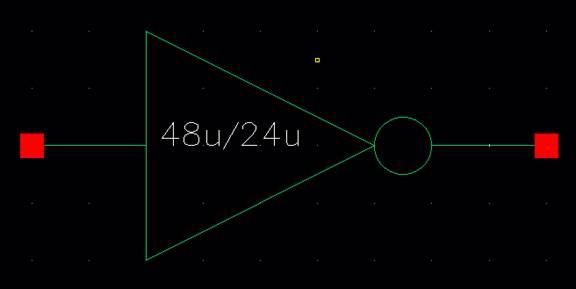
The second CMOS schematic is the 48u/24u where the device is using a
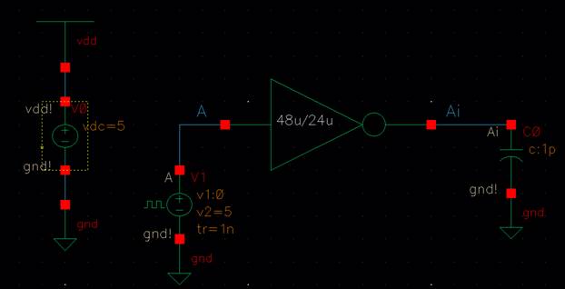
multiplier, M = 4. Here is the 4-terminal standard cell size:
Next is the symbol for the standard CMOS schematic:
Confirming the DRC for the 4x standard CMOS layout with no errors:
Verifying the LVS for the extracted layout with matching net-lists:
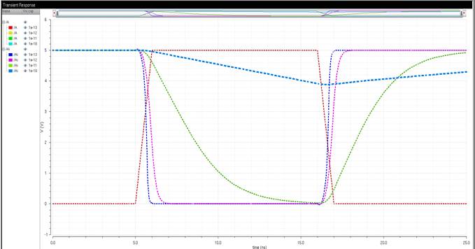
Now I have the simulation for the 48u/24u Inverter:
Graph displays for the inverter and the four capacitance outputs:
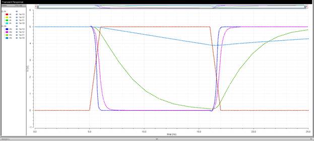
Ultrasim graphs for the 4x inverter:
Laboratory conclusion:
The results of comparing the two simulations between spectre and UltraSim for the Inverter and the 4X Inverter were similar. Depending on the value of the capacitance is what determines the CMOS to feature the abilities of an inverter, larger capacitances do not allow this, smaller ones do. The bigger CMOS is able to display bigger gains along with quicker rising and falling times graphically. The slightest adjustment of capacitance can have very strong effects on a circuit.