Matthew Daniel McDonagh NSHE:2001509804
EE-421 Fall 2021 Lab 3: Digital
Integrated Circuit Design
Layout of a 10-bit Digital-to-Analog Converter (DAC)
Pre-lab work: back-up all previous worm from the lab, finish tutorial 1.
The unfinished portion of tutorial 1 involves creating an N-well resistor in layout form, building the flowing circuit in a schematic layout and comparing this schematic to the one in layout by using LVS. Beginning by calculating what it takes to get a 10k resistor using the formula R = Rs(L/w) where R is the resistance required of 10k, Rs is the sheet resistance (~800 ohms), L and w are the length and width of the resistor with minimum length of 3.6um. Using this formula it is easy to choose a resistor with a specified length/width which will be used for the design of the N-well overall.
Formula: 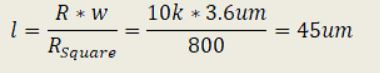
N-well layout:
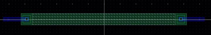
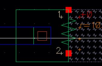
Continuing the steps in tutorial 1, the N-well is around 10.2k Ohms. The process of making the layout of the DAC is slightly simpler, The 2R and R voltage divider layout is created before the DAC here:
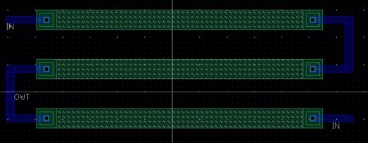
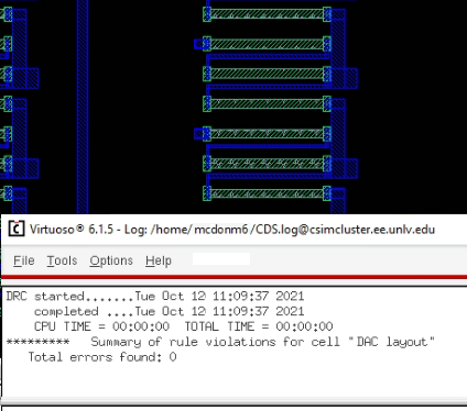
Here is the DAC of the layout in full view:
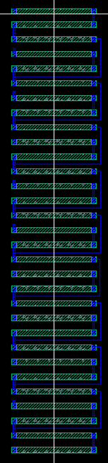 Image of top:
 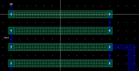 Image
of bottom:
Image
of bottom: 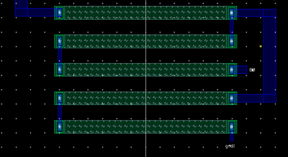
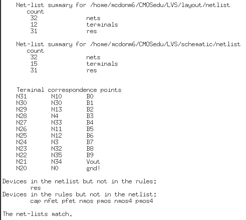
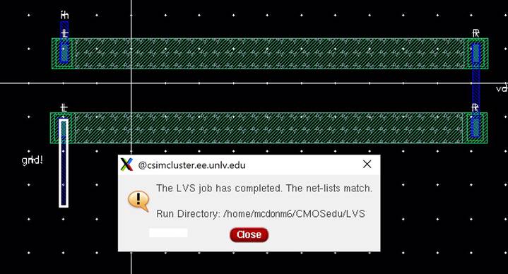
Testing the LVS:
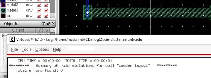
Verifying DRC Check:
Conclusion: After confirming the verifications for both LVS and DRC for this
lab, the last step is to back up my files to my google drive. I have done this
on my computer.