Lab 2 – EE-421L
Authored by Matthew Daniel McDonagh
EE-421 Fall 2021
email: mcdonm6@unlv.nevada.edu
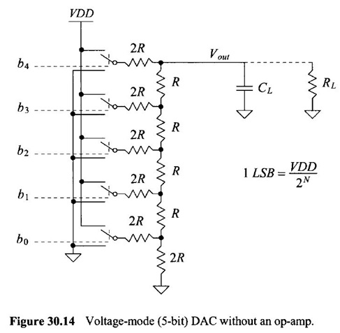
Lab description: In this lab we will be using n-well resistors to
implement a 10-bit DAC. This is a laboratory introduction to digital-to-analog-converters
as well as analog-to-digital converters. The design in this lab will be based
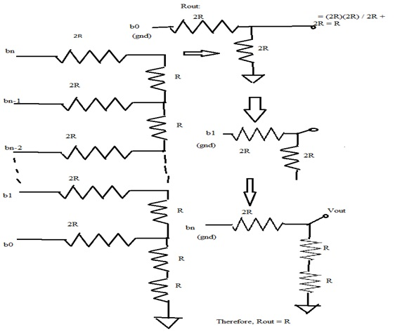
upon the topology seen in the figure below, which is also in the CMOS book.
CMOS technology allows multiple important implementations of these devices. The
controlling input bits in the figure below are from the ADC, meaning that the
inputs to the DAC are the left side of the 2R resistors. Implementation here is
achieved with the R-2R ladder:
Pre-lab work:
Continuing on with tutorial 1, place all files
in the proper directories using mobaXterm or terminal
application of choosing. The conceptual behavior behind the converters can be
elaborated on with a few short descriptions. Simple DAC
are implemented with R-24 string in voltage mode. For an ADC to collect
external information, analog signals must be converted to digital signals,
which is completed by sampling. An analog signal can be sampled without
aliasing (an effect that causes different signals to become indistinguishable).
The ADC range is max input to input, its precision is the number of
distinguishable inputs 2^N (where N is the number of bits). The ADC resolution
is the smallest distinguishable change in input V_in.max
/ 2^N where a change in input causes output to change by 1. Clock speed will
determine how quickly the converter can sample.
The accuracy of the sampling is computed in the following formula:
0.5 LSB / Full scale range (V_DD) = V_DD / 2^(N+1) * 1 / V_DD and the time
constant associated with the DAC and the capacitive load is r = RC_L. The
output formula for Vout = Vout.final(1-e^(-t/t))
the required setting time, t_setting = RC_L *
ln(2^N+1) and the max clock frequency, f_clk.max = 1/t_setting.
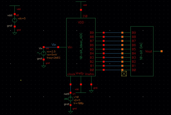
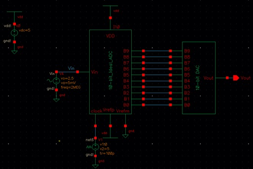
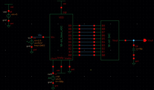
Opening the sim_Ideal_ADC_DAC schematic
under cell menu:
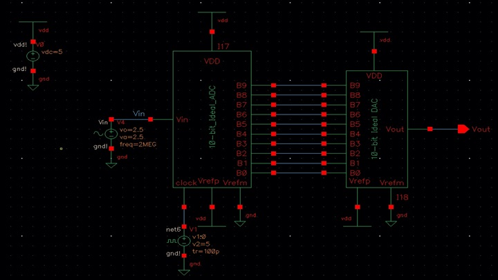
After running a simulation (following launchàADE LàSessionàLoad stateàCellviewàOKàGreen start button (simulation
of input of sin and no load):
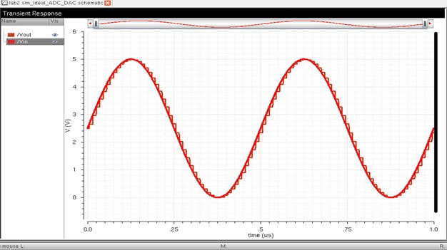
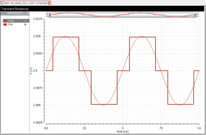
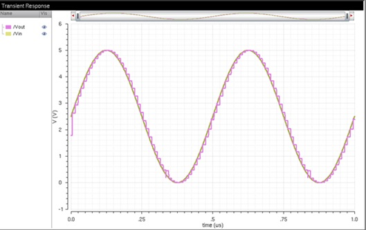
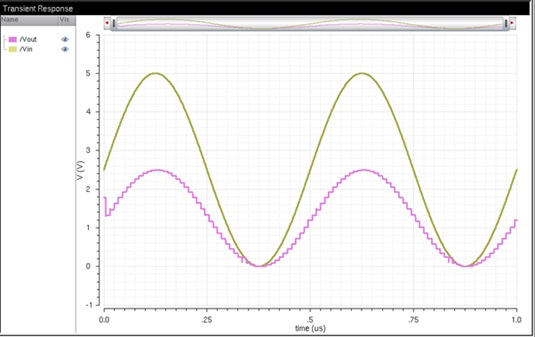
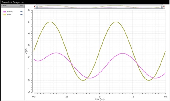
The simulation results above show the relationship between Vin and
B[9:0] is that the ADC takes the input from the Vin
and converts this input to a digital signal that produces a 10-bit binary value
which is then received by the DAC and outputs an analog signal Vout. To discover the least significant bit (LSB) we simply
use the equation shown below where we plug in our VDD and N: LSB = Vred / 2^N which delivers a value of Vout
to be around 5mV. That value represents the LSB and graph below:
This concludes the pre-lab portion.
Part 1: Creating a Digital-to-Analog Converter
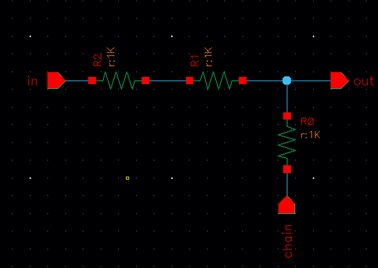
Beginning by creating a new schematic to fill in the ladder and
chain the 10 together:
Then creating a symbol for the schematic from cellview:
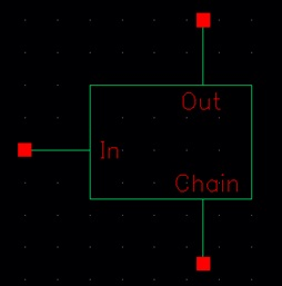
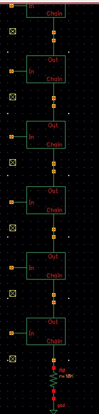
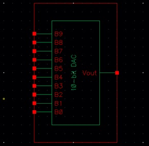
Using the symbol above to fill in a new schematic for the 10-bit
DAC:
top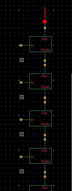
 bottom
To re-use the symbol which was created for the lab 2’s ideal
10-bit DAC, I copied it into the custom 10-bit DAC schematic. This is the
result:
Now to calculate output resistance
Rout:
Next calculating the delay with all
the pins to ground barring B9 with a capacitance of C = 10pF. The formula is: t_d = (0.7)RC à t_d = (0.7)(10k ohms)(10pF) = 70ns. The
maximum output voltage for this node is determined by the following formula: Vout.max = Vin*(R/(R+R)) = ½ * Vin where Vout = ½ Vout.max. By setting 2V
= Vin, at halfing that, we should see Vout.max = 1V and Vout = ½ Vout.max = 0.5V when the delay t_d
= 70ns.
Here is the DAC design:
Corresponding circuit:
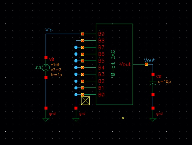
Now creating sim2_ideal_DAC and
replacing the DAC component with our own:
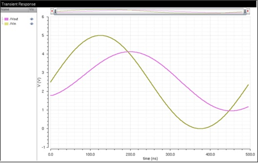
Here is the circuit under no load and
its simulation result:
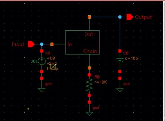
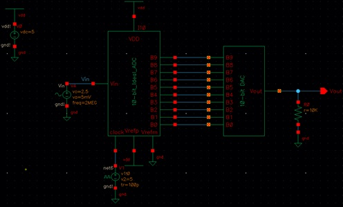
Here is the circuit under a 10k
resistive load and its simulation result:
Here is the circuit under a 10pF
capacitive load and its simulation result:
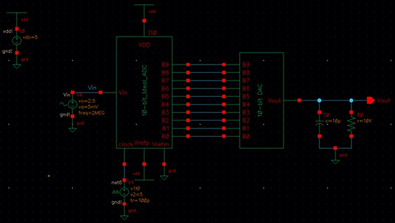
Here is the circuit under both a 10k
resistive and 10pF capacitive load, and the resulting simulation:
Conclusion: Compared to the value of
the resistance R, if the switches are transistors or the resistance value of
the switches is larger than R, there would be a different equivalent resistance
of DAC. An equivalent resistance value that is larger than R would be caused by
the resistances in series being higher themselves. The smaller output voltage
value (Vout) would be caused by a higher resistance
from the larger voltage drop across the transistor. Each new equivalent
resistance value must be calculated and considered for the load of the 10-bit
DAC. These simulations show that the DAC works as expected. Without a load there
is simply a tiny lag, with a resistive load only the output is halved, with a
capacitive load only the output resolves smoothly with a delay, and when both
are present the DAC’s output experiences minimal lag and a reduced voltage
value.
I will back the work up on my google
drive as instructed.