Lab Project - EE 421L
Authored
by Adrian Lopez-Macuaran,
lopezmac@unlv.nevada.edu
November 21, 2021
Project DescriptionFor this project we are designing a register file (RF) that contains 32 words and each word contains 8-bits.
-The RF utilized a 5-bit address using a 5-input NAND gate in order to determine which of the 32 words are being accessed.
-8 input and output lines will be utilized for reading and writing.
Project Procedure
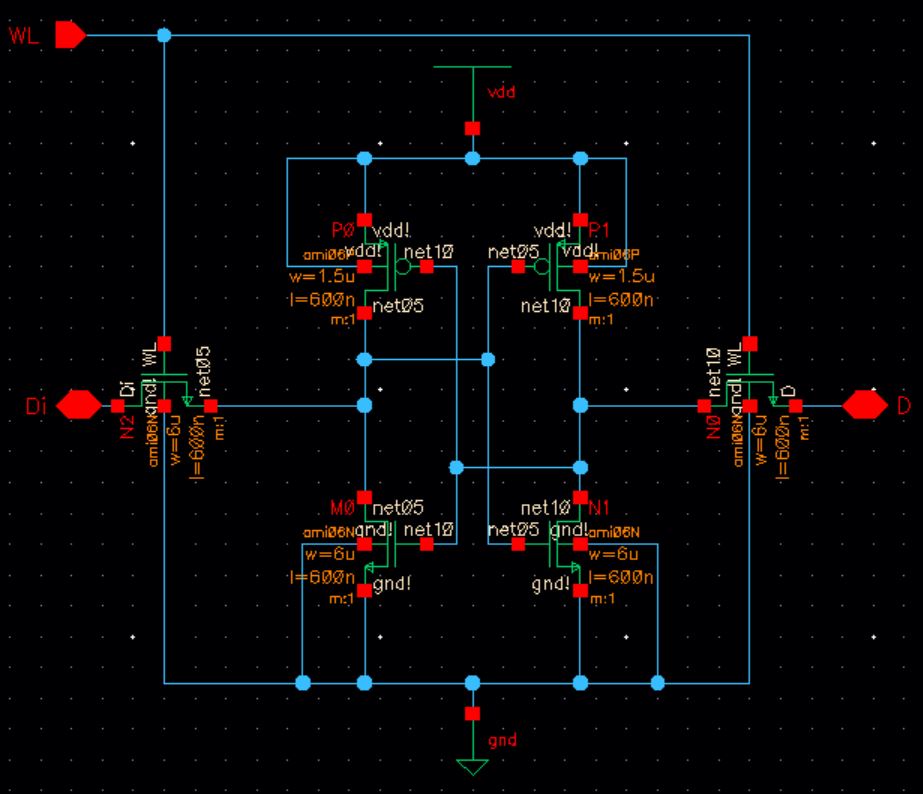
SRAM Cell
the
firsrt part of the project design is making the Static Random Access
Memory (SRAM). This cell contains 1-bit of data. The SRAM is made of
two inverters sized 1.5u/1.5u, and two NMOS transistors. The NMOS transistors are used because NMOS cant pass logic '1' well.
SRAM Schematic
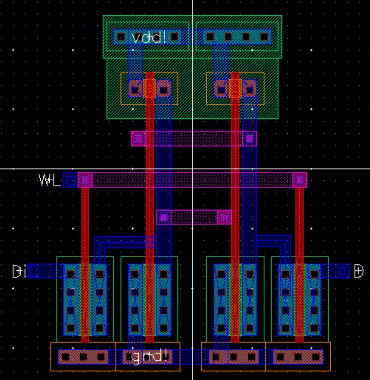
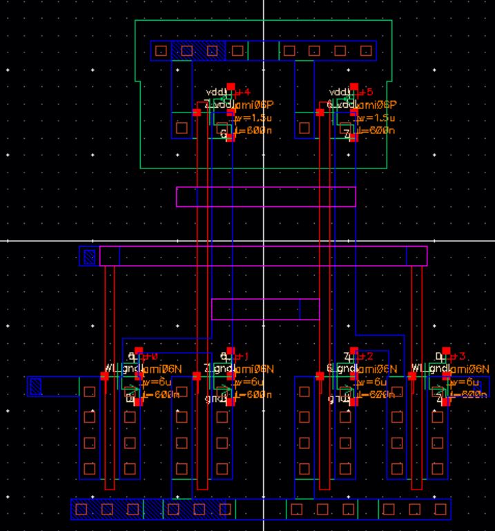
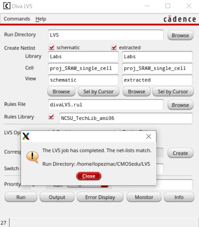
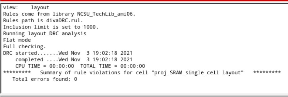
The following will show the layout,extract,DRC,LVS, and symbol of the SRAM Cell
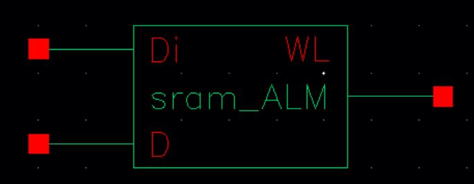
SRAM Symbol
Following I will show The Simulation schematic and results.
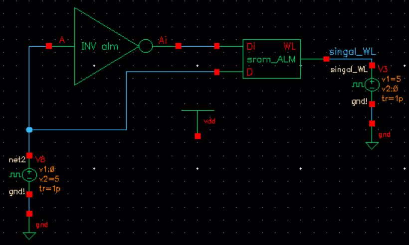
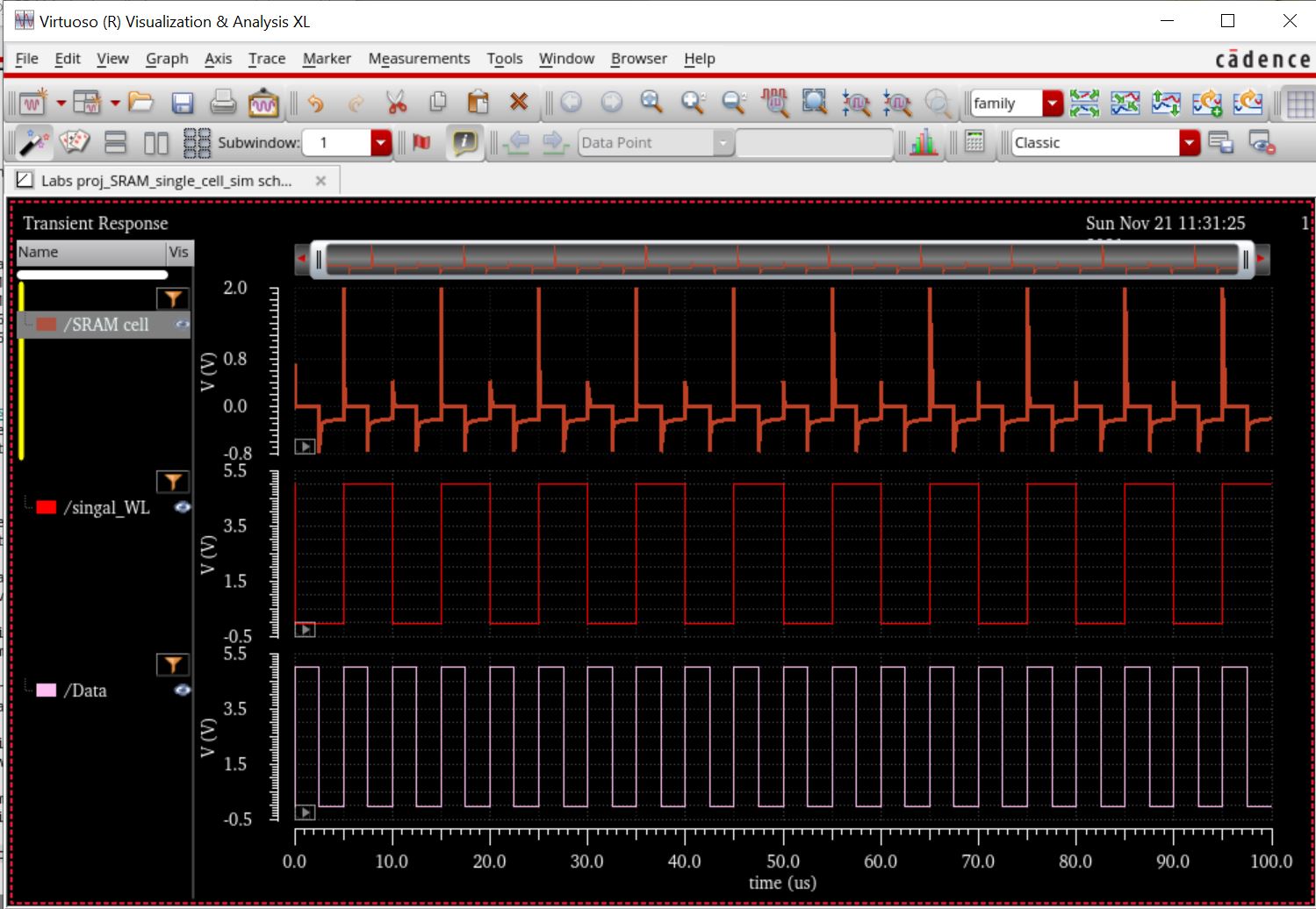
From the results we can see the SRAM is working as expected storing data when the word line is a logic '1'.
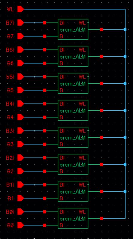
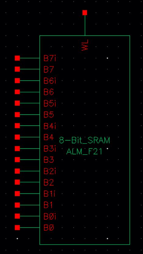
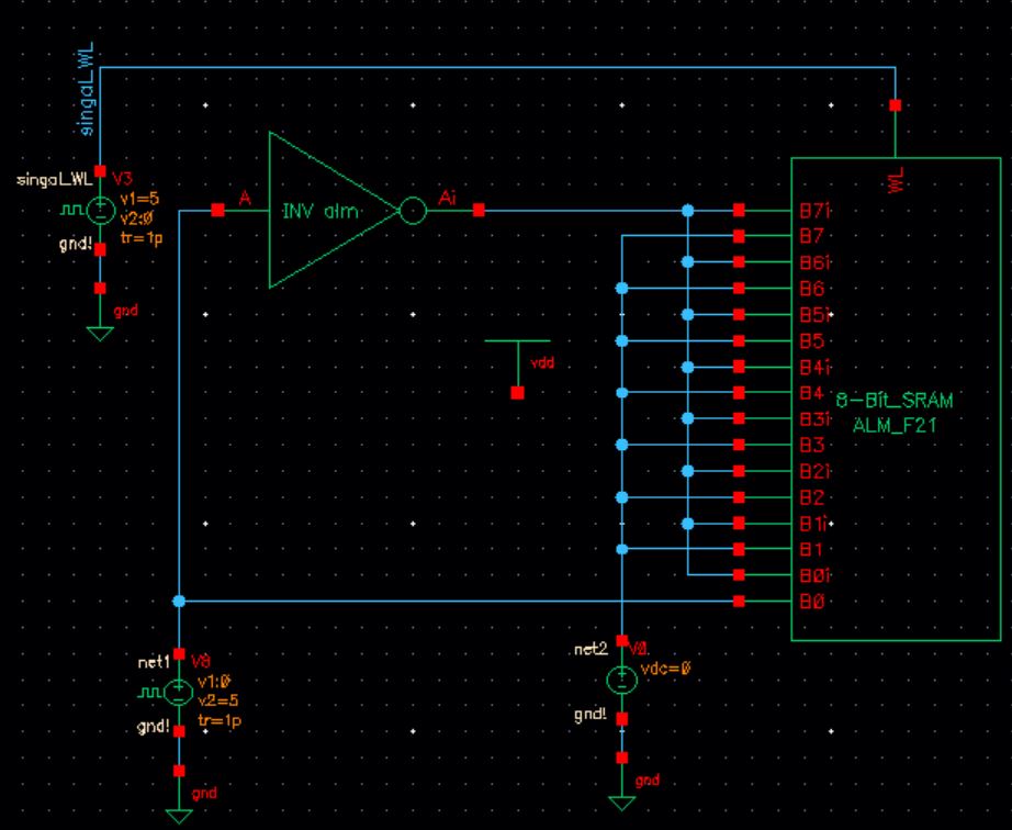
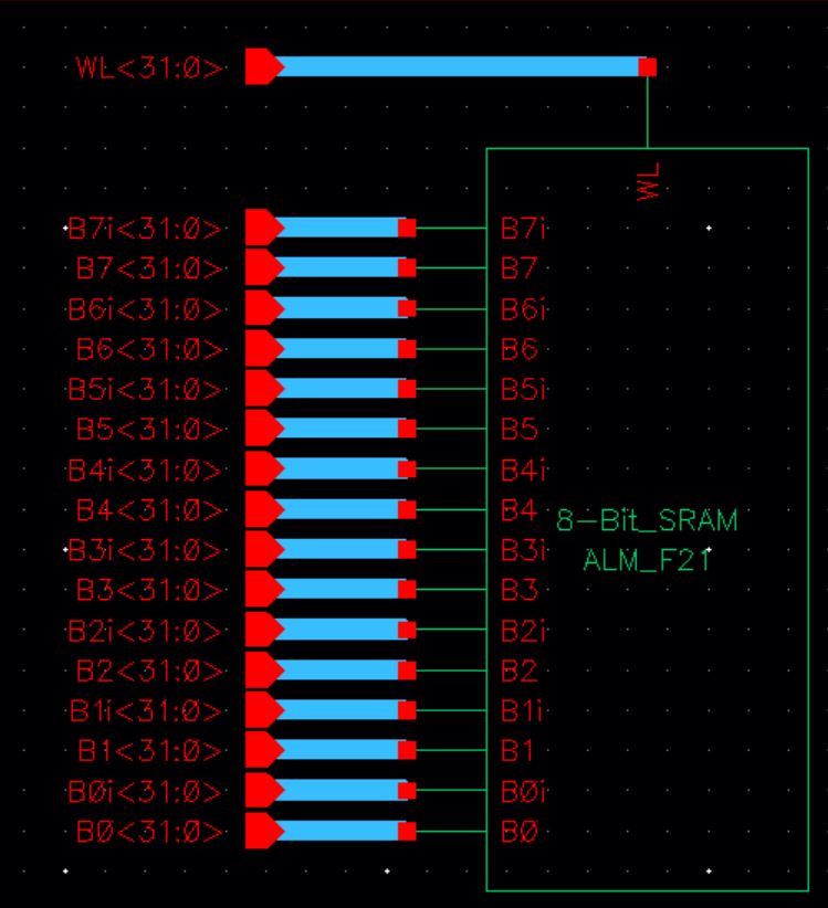
8-Bit Word Schematic and symbol
Our word is made from 8 SRAM cells.
Following I will show the Layout, Extract, DRC, LVS
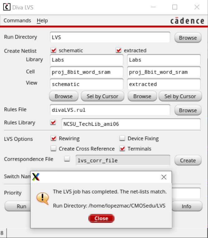
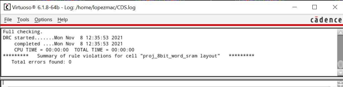
Following I will show The Simulation schematic and results.
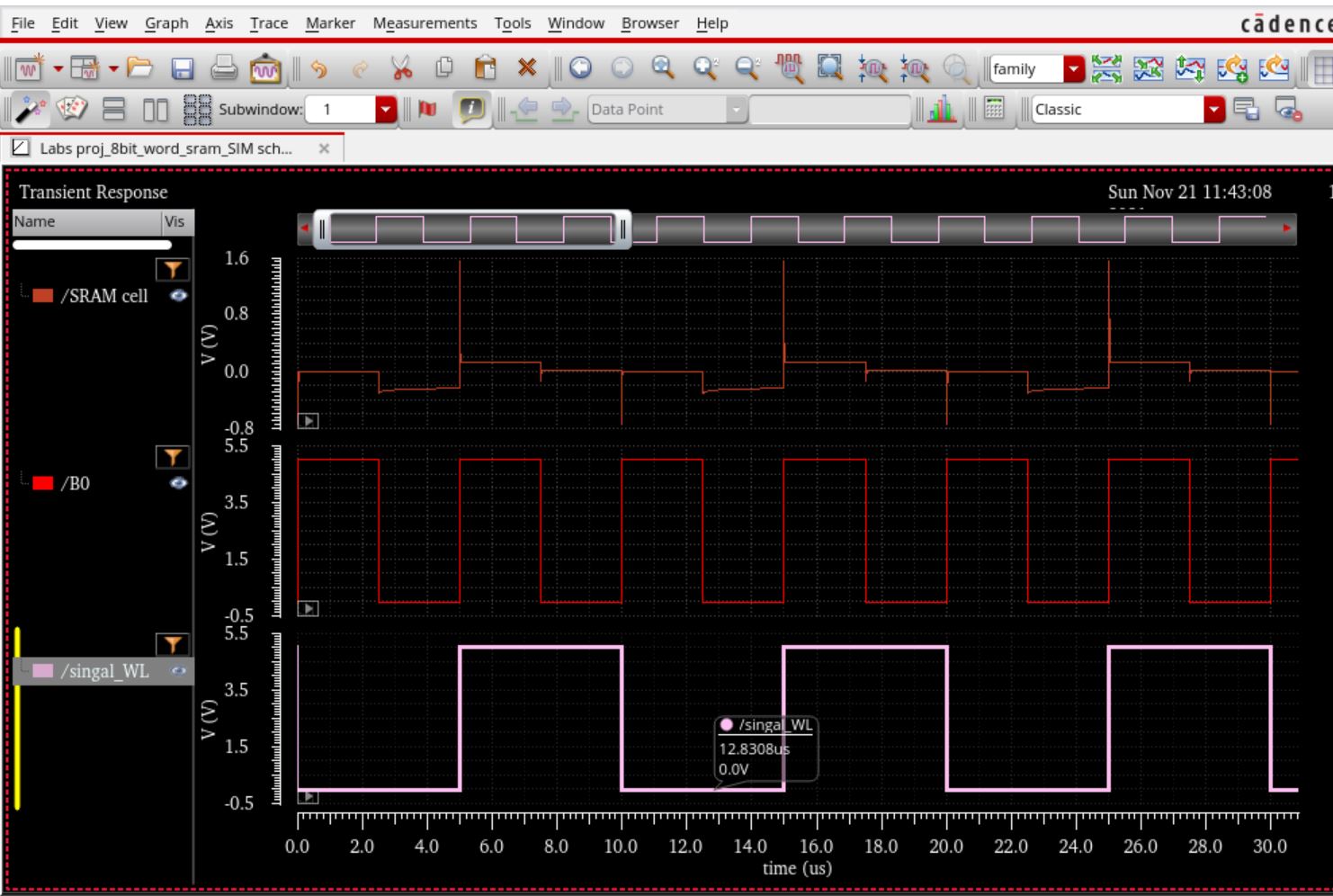
From the results we can see
the SRAM is working as expected storing data when the word line is a
logic '1'. In this case as well we are looking at the work located at
B<0>.
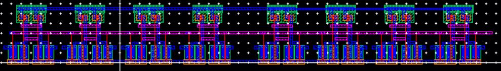
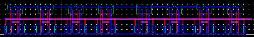
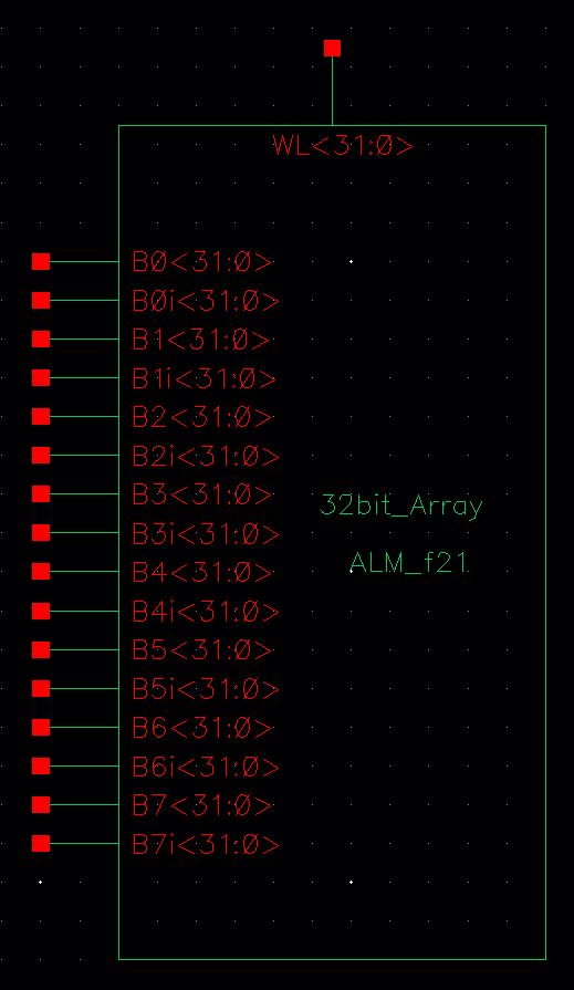
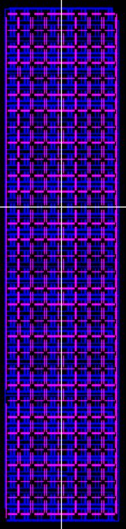
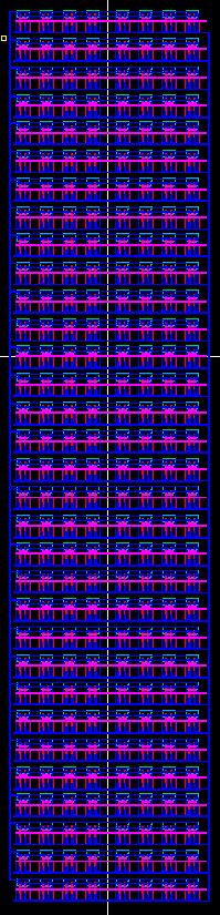
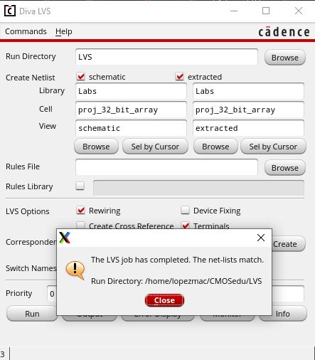
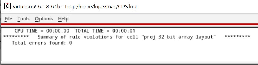
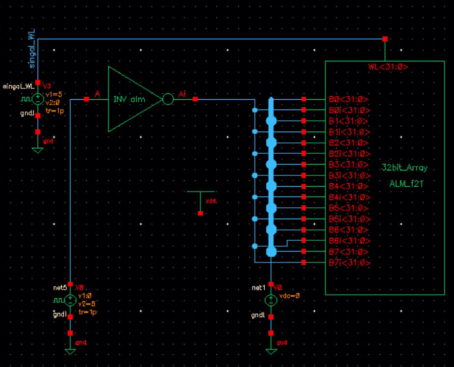
32-bit Word Array and Symbol
32-Bit word is made from the 8-bit word previously made. This array lets us know what word is being accessed.
Following I will show the Layout, Extract, DRC, LVS
Following I will show The Simulation schematic and results.
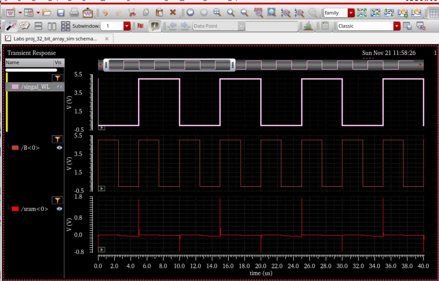
From
the results we can see the SRAM is working as expected storing data
when the word line is a logic '1'. In this case as well we are looking
at the work located at B<0>.
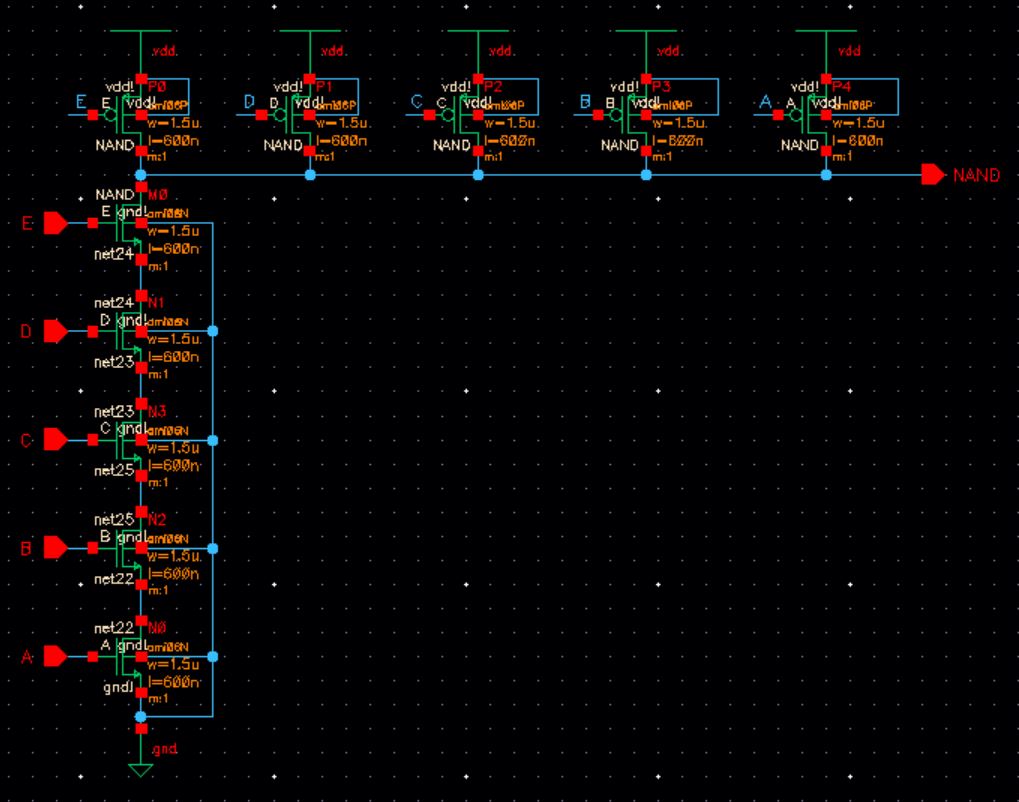
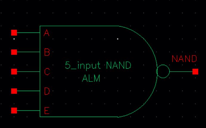
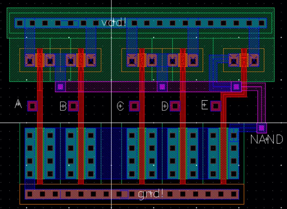
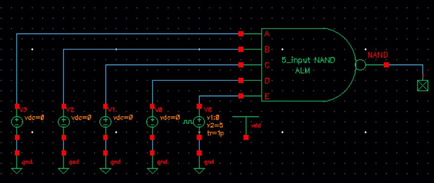
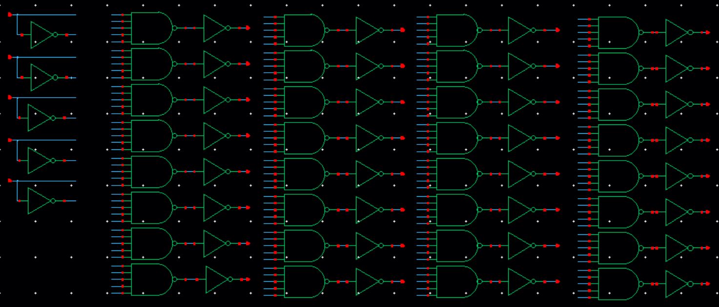
5-input NAND Gate and Symbol
The NAND Gate will be used to help implent the Row Codecoder having 5-inputs and one output.
Following I will show the Layout, Extract, DRC, LVS
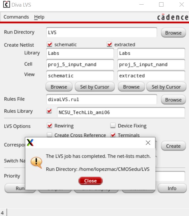
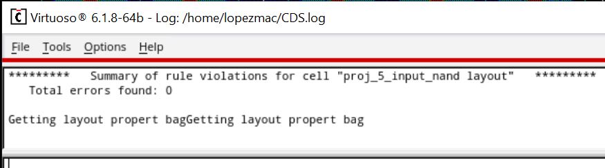
Following I will show The Simulation schematic and results.
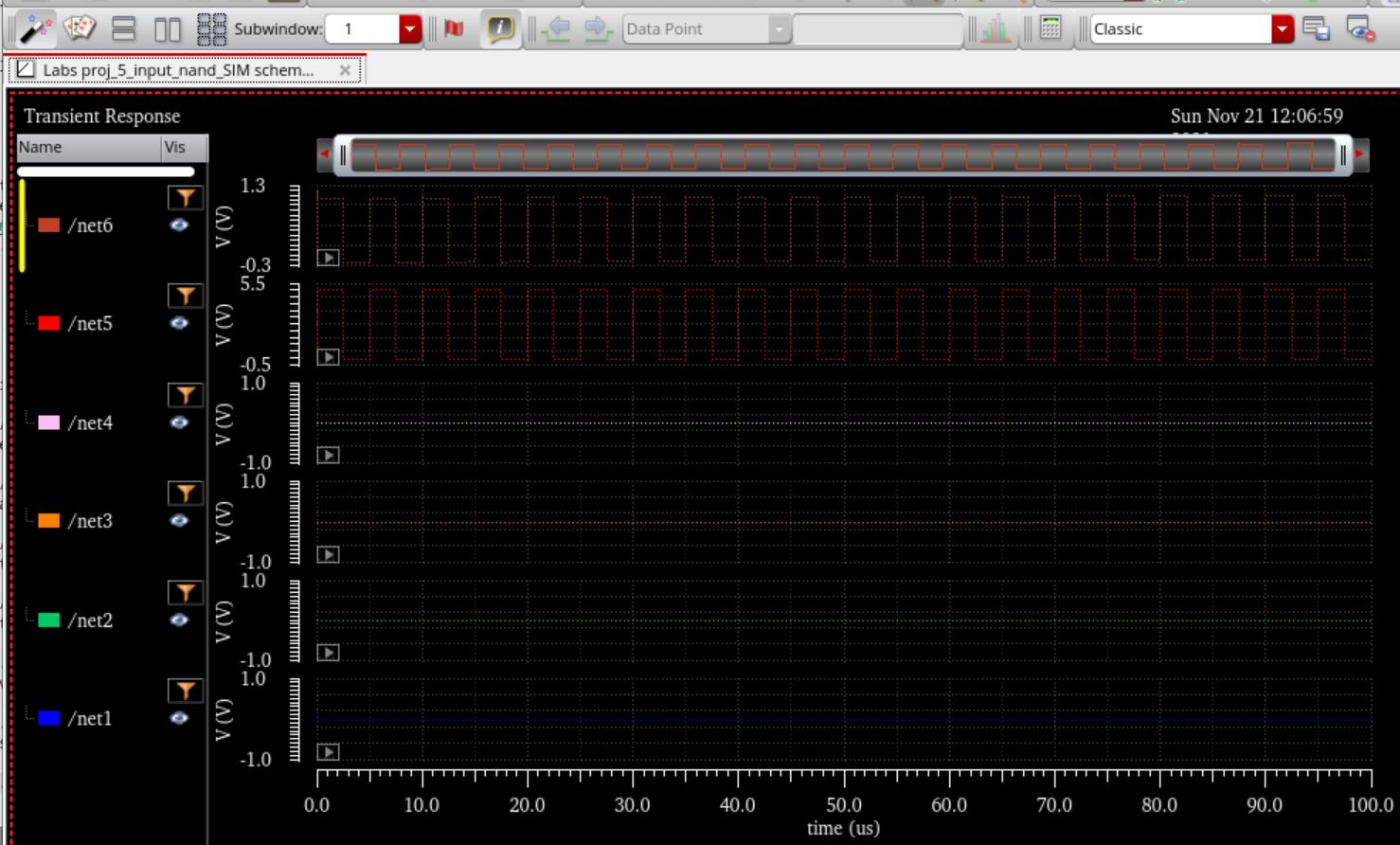
The results show that the nand gate is working as expected
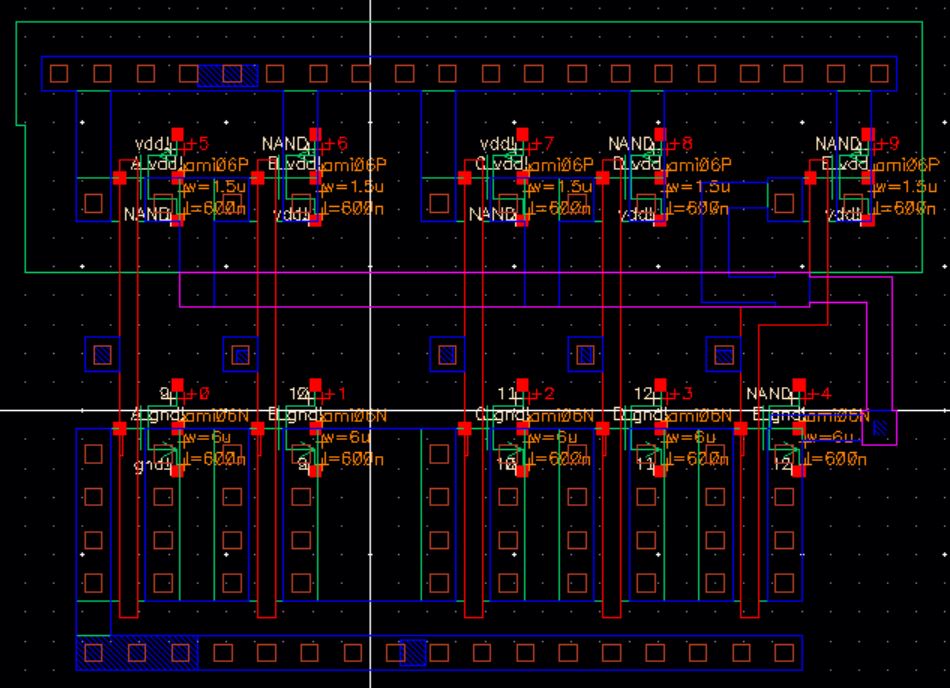
Row Decoder with a zoomed in portion
The row decoder lets us know what 8-bit cell is being accessed.
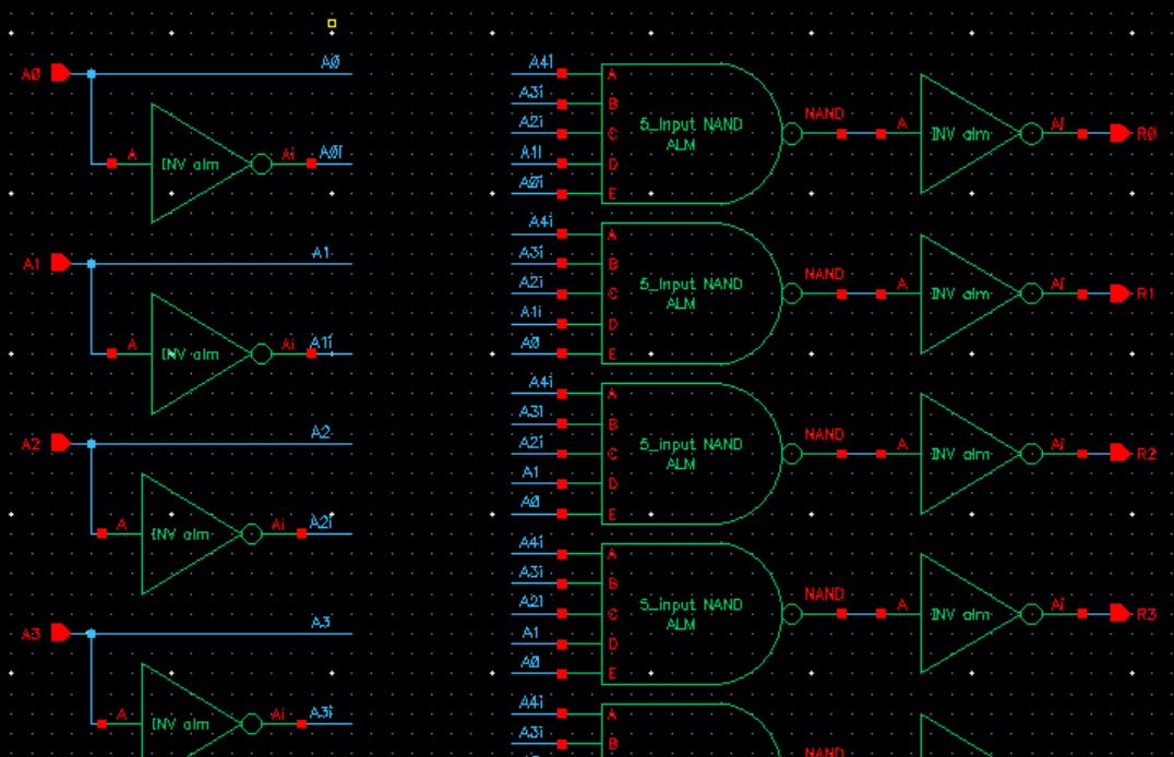
Following I will show the Symbol, Layout, Extract, DRC, LVS
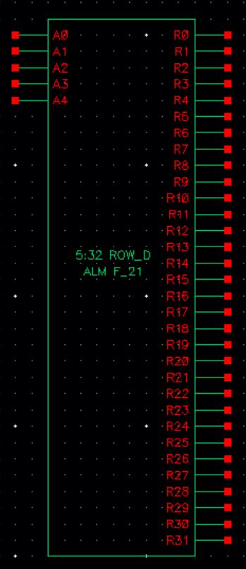
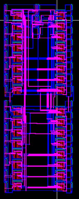
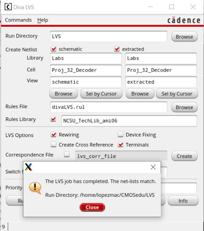
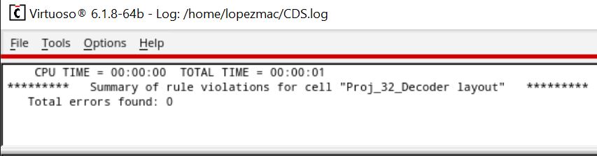
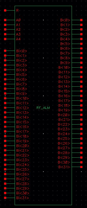
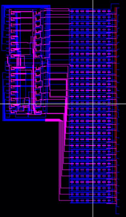
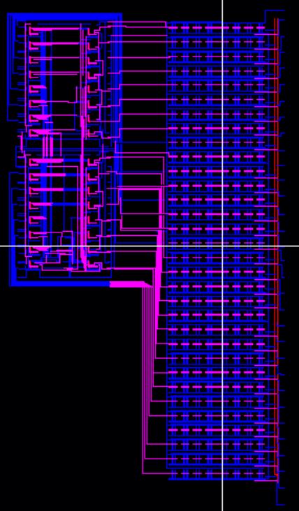
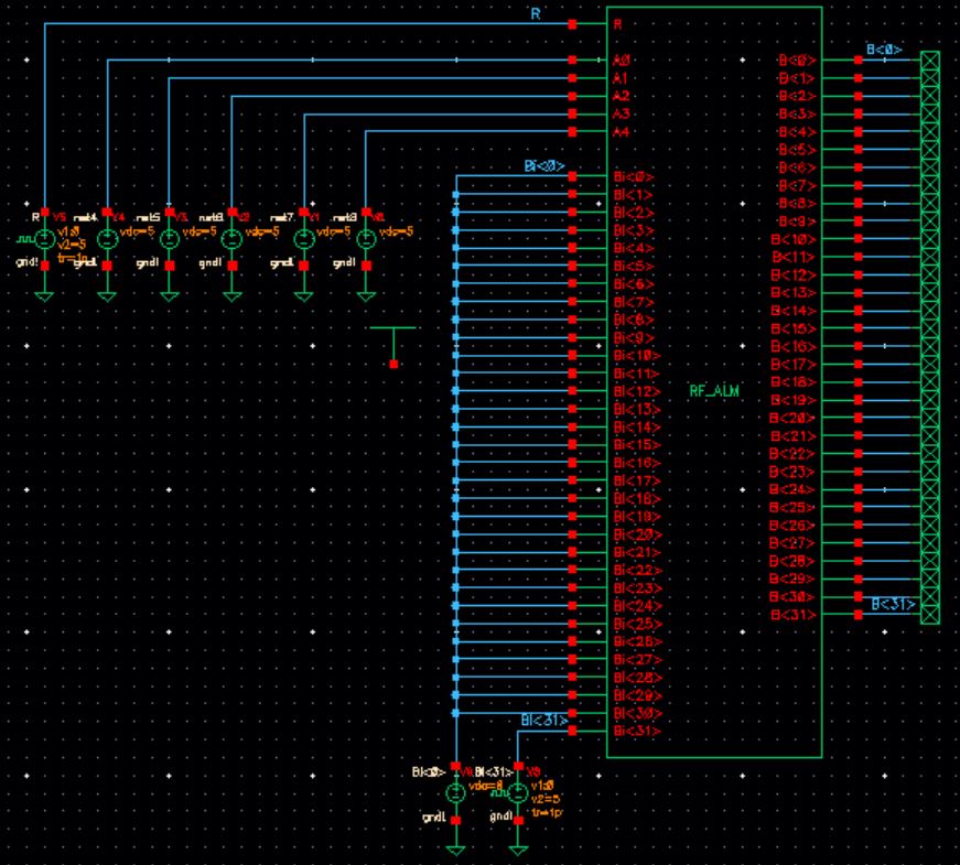
Register File (RF) and Symbol.
The RF is made up of 32-word array, 8-bit Word, SRAM, and Row Decoder.
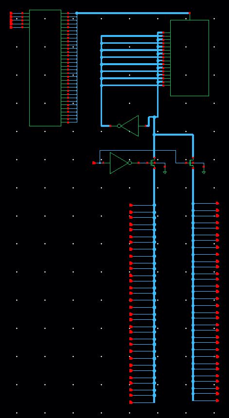
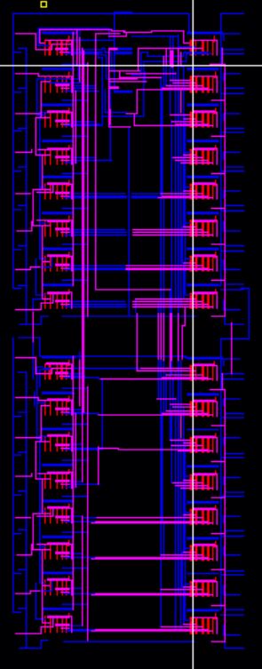
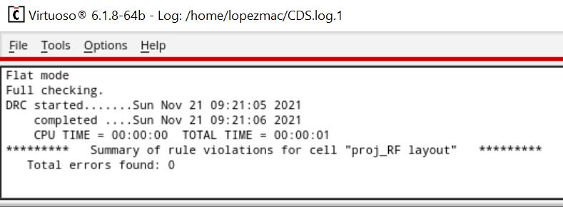
Following I will show the Layout, Extract, DRC, LVS
RF Simulations
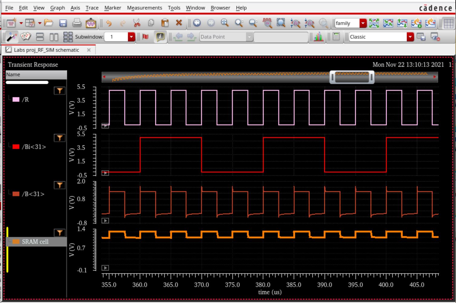
From
the Word Line(R) pulsing from 0-5 causes the RF to write when its a
logic '0'. Bi<0> will be written into the adress 11111 cell. When
the Word line changed to a logic '1' the RF will be in read mode and
the value in 11111 will be the ouput for B<0>.
Conclusion
From
the results of my simulaiton are correct, the issue I had was my ouput
was not ouputting the whole 5v. While reading more about RF the
solution to this to incorporate a charge line to cause to achieve full
logic levels.
RF Project Zip File
Rf_zip
Return to Labs