Lab 3 - EE 421L
Authored
by Adrian Lopez-Macuaran,
lopezmac@unlv.nevada.edu
September 8, 2021
Lab
description
For this lab we are to layout our 10-Bit Digital to Analog Converter we designed in our previous lab.
Pre-Lab
For
our pre-lab we were to finish tutrial 1. From our previous lab, lab 1,
we had started tutorial 1 up to image 25 on the tutorial, now we are to
finish tutorial 1 which is the layout of a voltage divider and LVS of
our design.
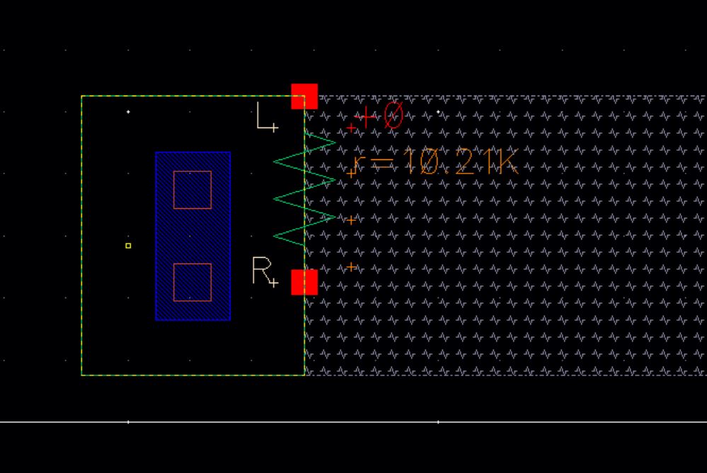
The
following will show the layout of the voltage divider. We use the
n-well layer to create our resistor and chose the correct legngth and
width. For the reistor to work we must put the 'RES id' layer to cover
the size of the n-well. For the ends where the pins are placed we use
Ntap. It is important to keep in mind that For LVS to work you must
name the pins on the layout the same as on the schematic. After the
layout was complete we extract the layout then LVS it against our
schematic.
LVS of above layout.
Lab Task
- Use the n-well to layout a 10k resistor as discussed in Tutorial 1
- Discuss,
in your lab report, how to select the width and length of the resistor
by referencing the process information from MOSIS
- Use this n-well resistor in the layout of your DAC
- Discuss, in your lab report, how the width and length of the resistor are measured
- Ensure
that each resistor in the DAC is laid out in parallel having the same
x-position but varying y-positions (the resistors are stacked)
- All input and output Pins should be on metal 1
- DRC and LVS, with the extracted layout, your design (show the results in your lab report)
- Zip up your final design directory and place it in
the lab3 directory, with a link on your lab report, so the grader can
examine both the layout and schematic (and simulations)
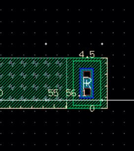
Use the n-well to layout a 10k resistor
For
creating the 10k n-well resistor we were to select the correct
lenght and width. For my desing I picked L= 56.1um and W= 4.2um. I now
placed the these values in our formulas to calculate resistance. We
should remember that the sheet resistance is equal to 800 ohms/square.
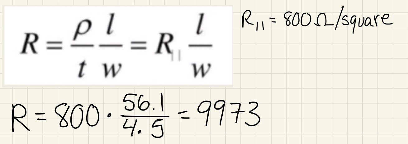
From
the above equations we calculated our resistance around 9943 ohms. To
measure our layout we press 'k' to bring up the ruler and 'shift k'
will erase the ruler.
After extracting the layout to check the value of the resistance we get a resistance of 10.2K ohms.
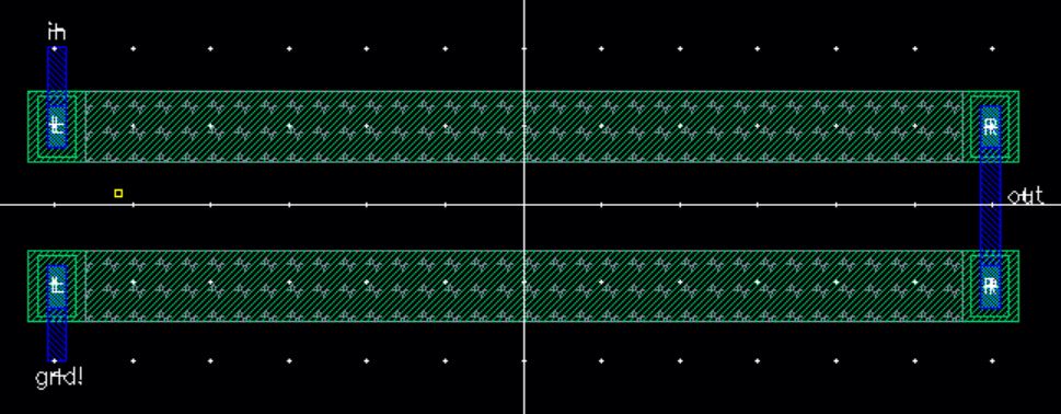
Use this n-well resistor in the layout of your DAC
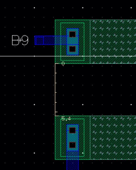
I
start the layout by place our votage divider layout then copying
various as needed each 5.4um appart from each other. Each divider
represents a bit. Then I labed each bit using pins on metal1, B9-B0,
and also labling Vout and Gnd. The following will show the spacing and
the final layout of the 10-Bit DAC.
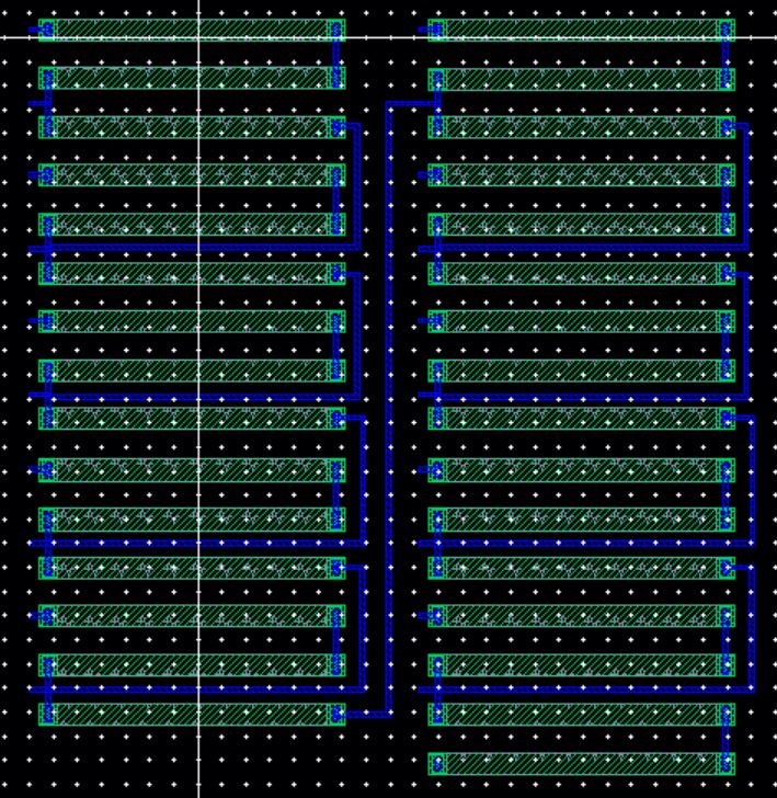
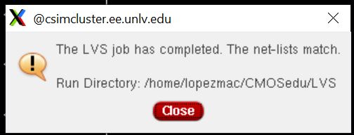
DRC and LVS, with the extracted layout
Next I will show the extracted view of my layout and the DRC and LVS.
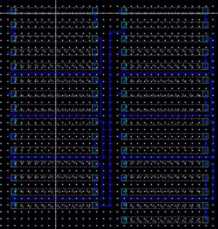
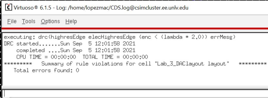
The
above pictures show the extracted view of the 10-Bit layout and shows
the DRC with no errors. Next I will LVS the design. To LVS you compare
the schematic vs the extracted layout. My schematic was in Lab_2_DAC
and my layout in Lab_3_DAClayout.
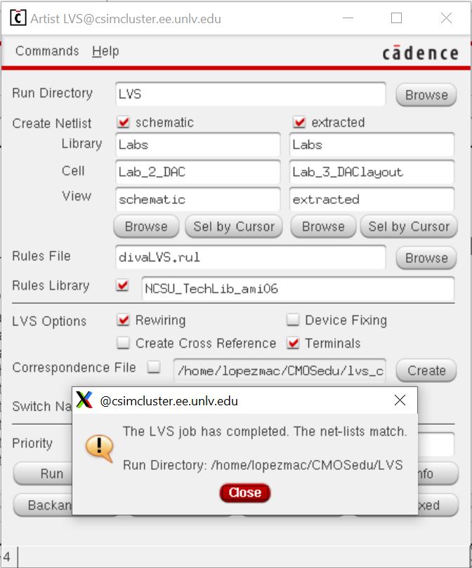
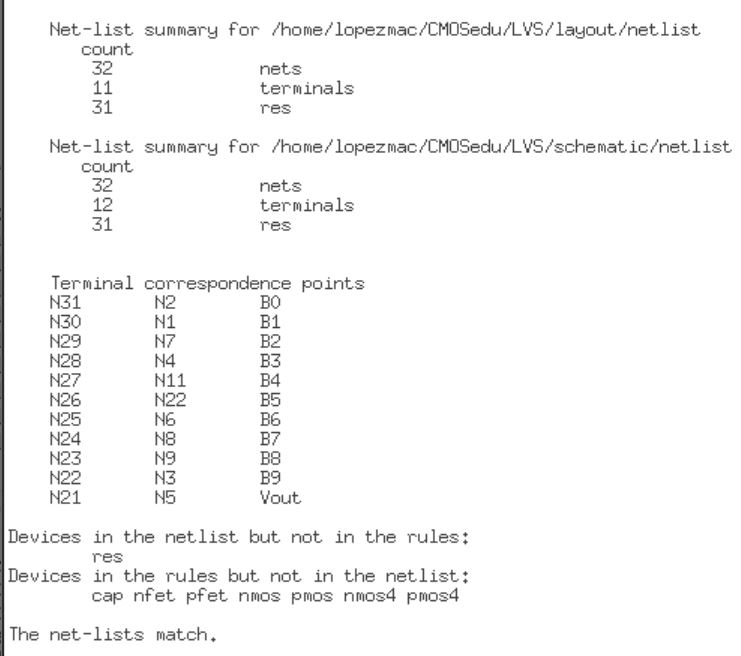
From the above pictures we can see that our net-list match and the LVS was successful.
Lab_3 folder design zip
The schematic design is under Lab_2_DAC and the layout is under Lab_3_DAClayout
lab3.zip
Backing up work
As always I backed up my work twice once for the pre-lab and once after the postlab.
Return to Labs