Lab 2 - EE 421L
Authored
by Adrian Lopez-Macuaran,
lopezmac@unlv.nevada.edu
August 28, 2021
Lab
description
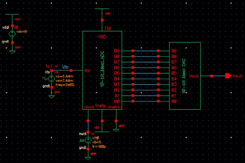
For this lab we covered the desing of a 10-bit digitial-to-analog converter (DAC).
Pre-Lab
- Prior to coming to lab make sure you understand how the input voltage, Vin, is related to B[9:0] and Vout (the quiz may ask a question about this).
- In
your lab report: 1) provide narrative of the steps seen above, 2)
provide, and discuss, simulation results different from the above to
illustrate your understanding of the ADC and DAC, 3) explain how you
determine the least significant bit (LSB, the minumum voltage change on the ADC's input to see a change in the digital code B[9:0]) of the converter. Use simulations to support your understanding.
- Backup your webpages and design diretory.
Pre-Lab Procedure
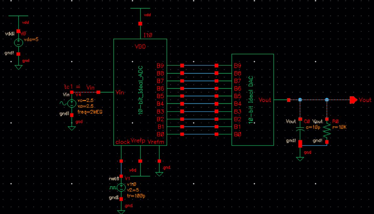
The
first step to this pre-lab was to download the file (lab2.zip)
and uploaded and unzip it to the CMOSedu dicrecotry. Next we
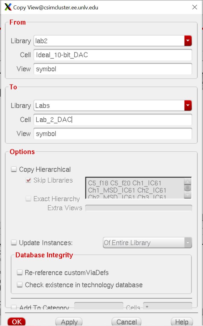
define the the folder in our cds.lib.
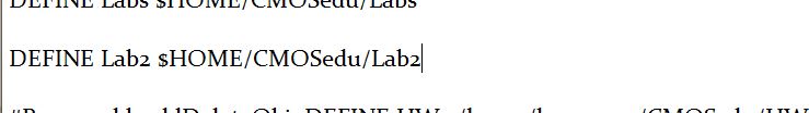
Fig.1 Shows lab2 defined in our cds.lib
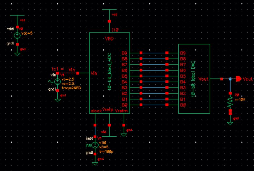
Next we opened the library lab2 then proceded to open the schematic.
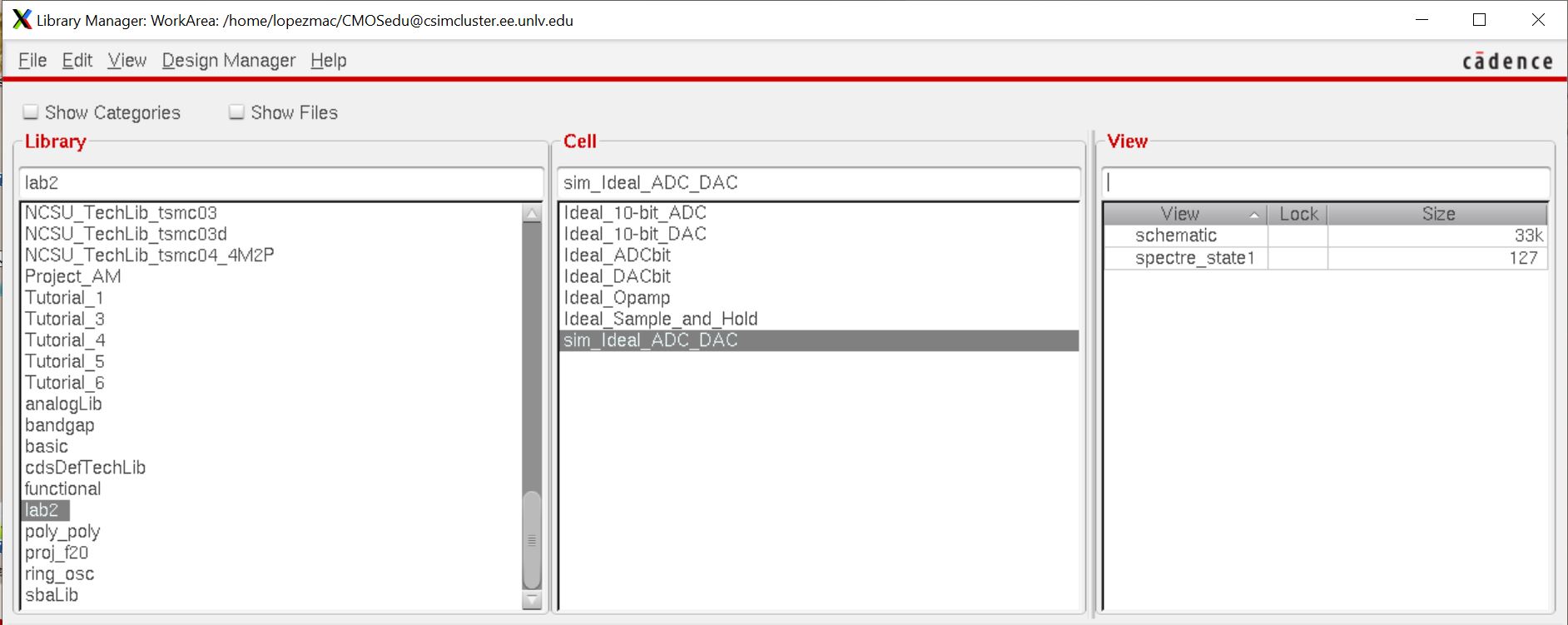
Fig2.1 shows the lab2 was successfully unziped.
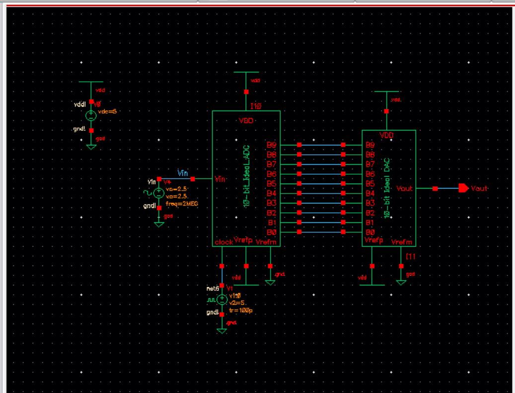
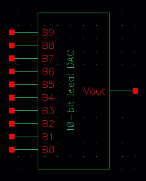
Fig.3 (DAC) Schematic.
After
we open the schematic we launch ADE L which stands for analog design
environment. After launching ADE L we click on session then click on
Load State. From here we select cellview then click ok. Once the screen
loads we are good to run the simmulaiton by pressing the green arrow
button.
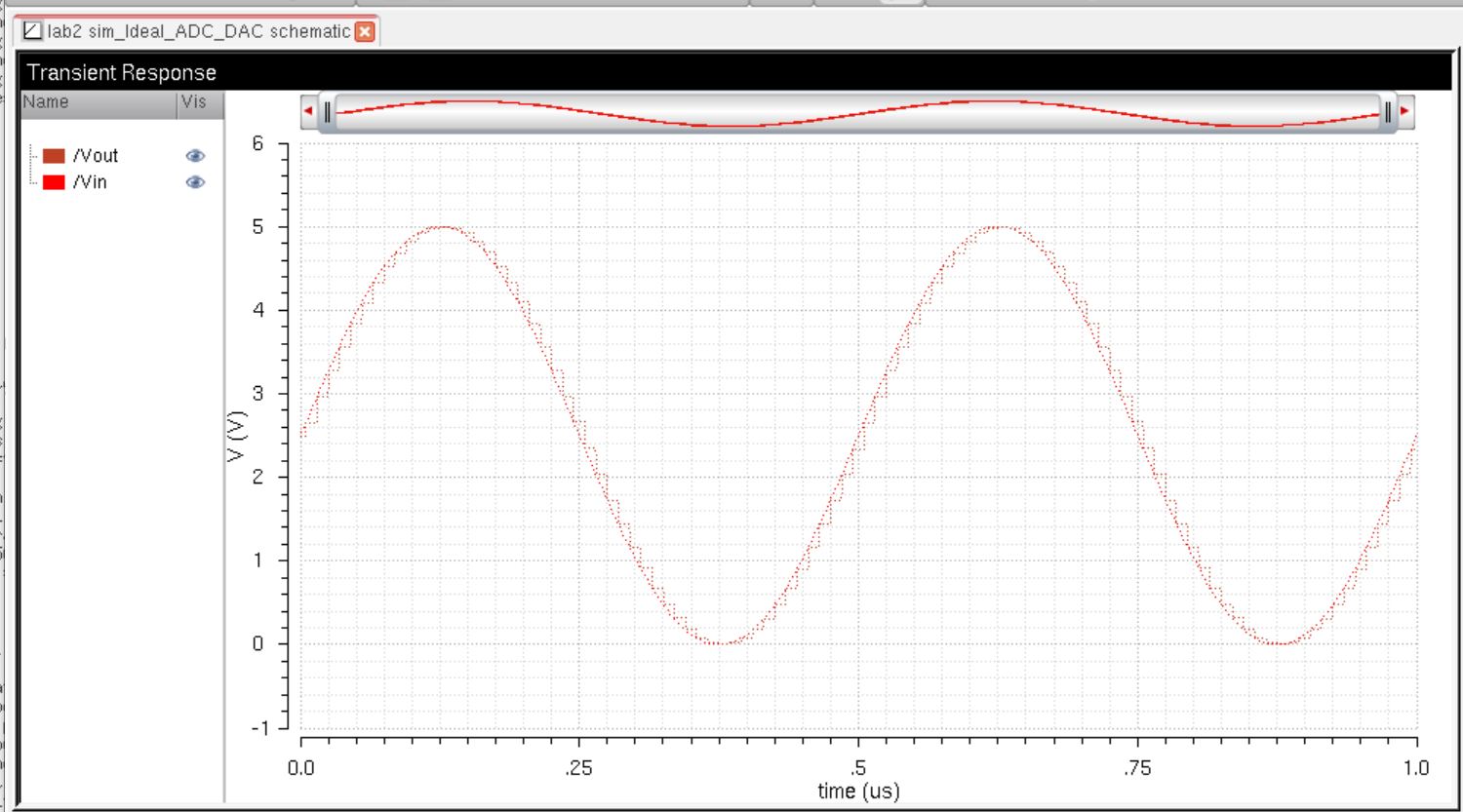
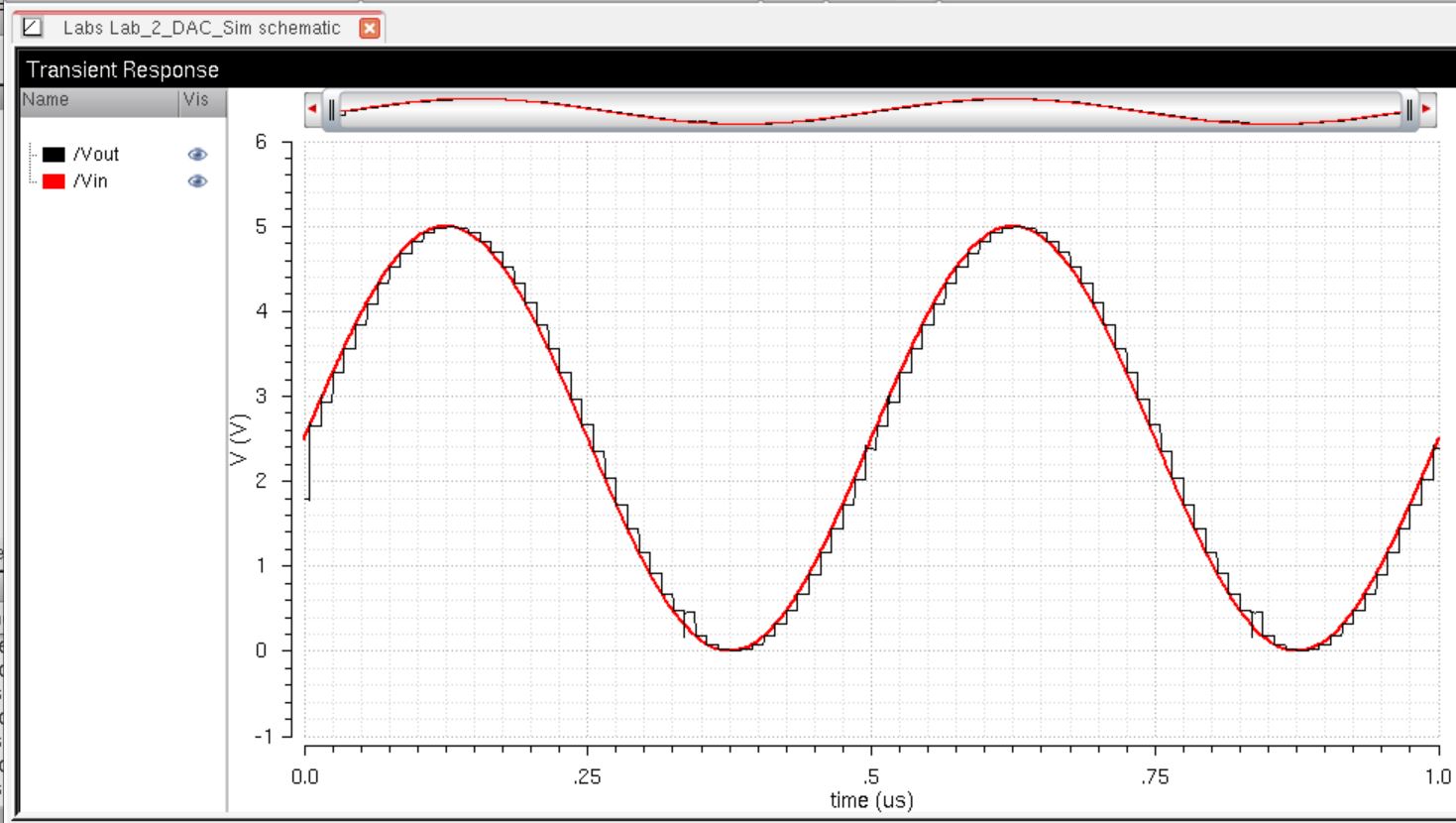
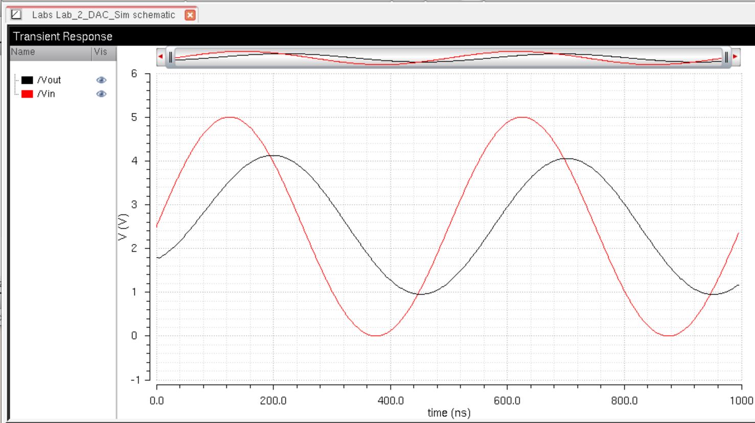
Fig4. This shows our simulation results
Next
we were to familiarize our selves on how to edit our graph and line
type. To edit graph we simply right click and select graph properties,
this lets us change the background color. To edit our line types we
click the line we want to edit and right click then select trace
properties, from here we can change line thickness, line type, and line
color.
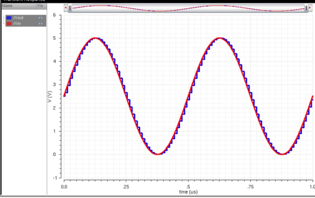
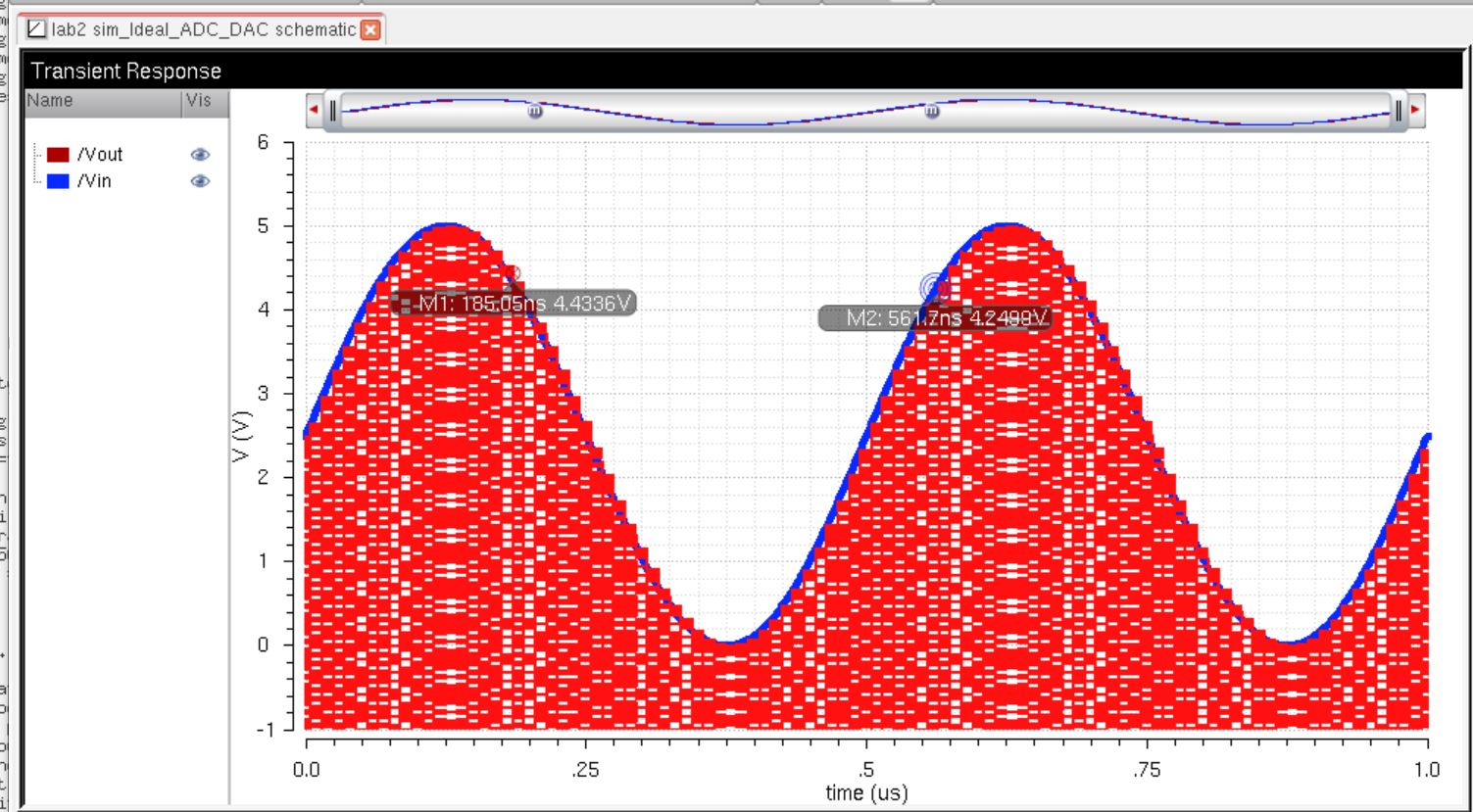
Fig.5 the aboe figures show two different ways one could edit their simulations vin(red) vout(blue)
From
the above simulation results we can see that the output signal has many
incremental steps and we cannot observe the graph results clearly. To
fix this we can set the input voltage to 10mV with and offset of 10mV.
To do this we go back to our schematic select the input voltage and
press (q) to bring up properties input our valuse then press ok, then
check and save and finally re-run our simulation.
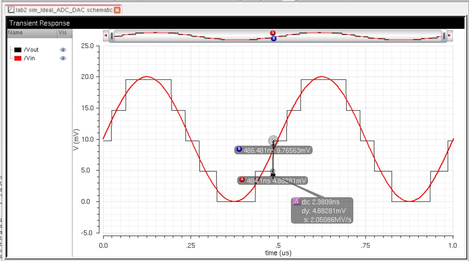
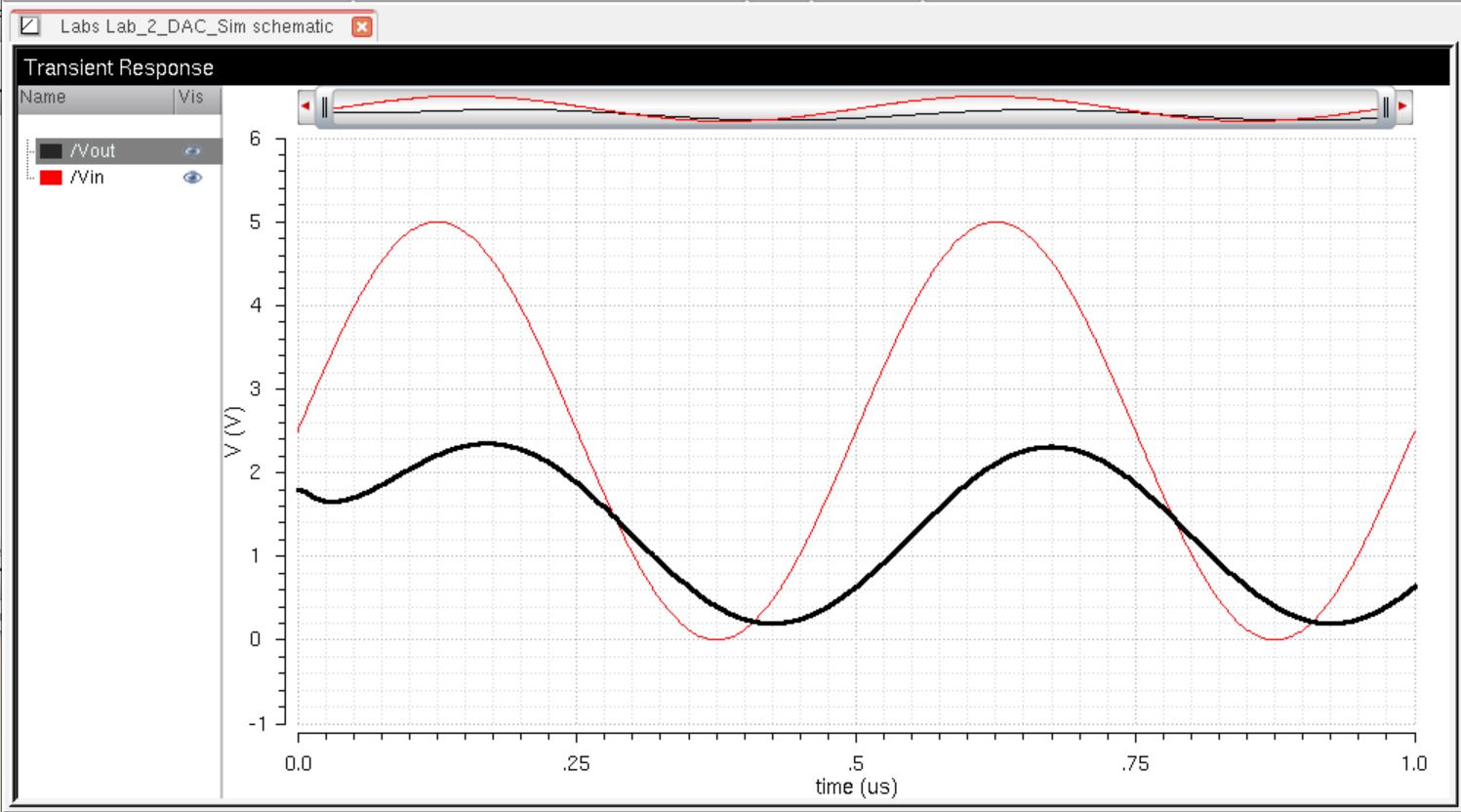
Fig6. Shows a much clearer result
From
the above result I also place to markers on the graph. Pace a marker on
the bottom of the step, I did this by selcting the area I wanted a
marker and pressing 'A'. Then I place a marker 'B' at the top of the
step. This gave us a dY of 4.88281mV which indicates the Least
Significant Bit (LSB). We know this to be true because LSB represents
the minimum change on the ADC input required to show a change in the
ouput. Using the following Equation we can also fing LSB. Step
size = Vcc / 2^N
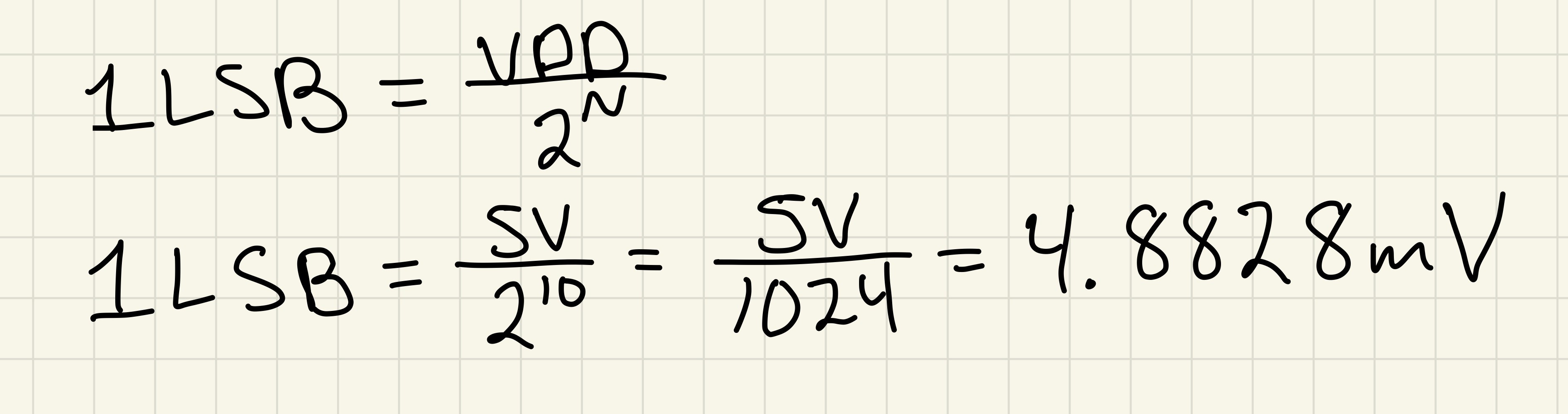
Fig7. Show how to hand calculate LSB and shows the markers gave us the correct dY
Next
we can change our properties in our schematic one more time to get a
more accurate step size. We do this by changing out propreties in our
input to have an amplitude of 2.44mV and an offset voltage of 2.44mV.
After we change the input we click and save then run our simulation.
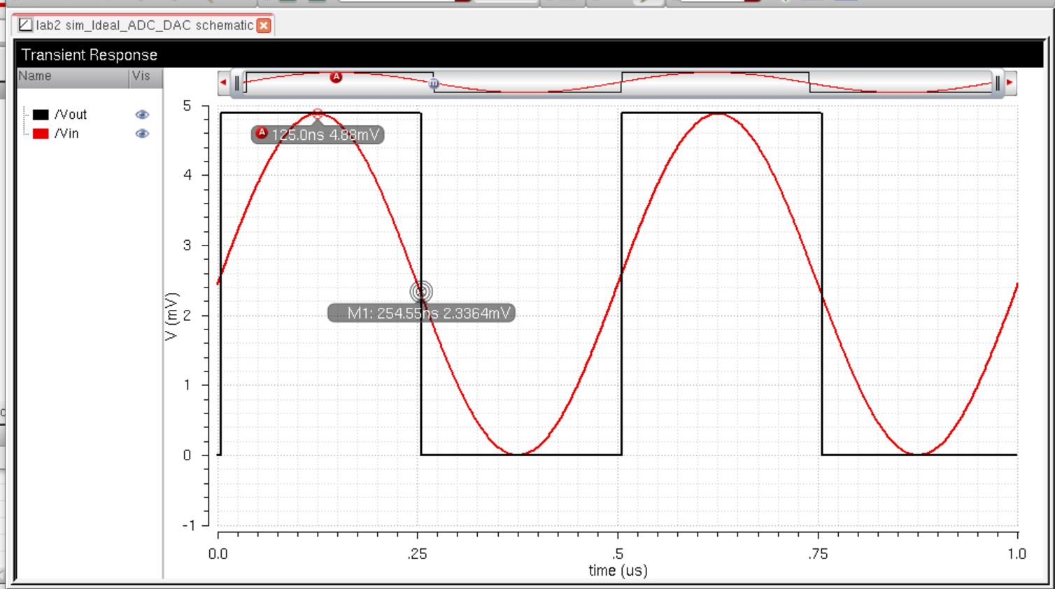
Fig.8 shows the correct step size
Lab Tasks
- Design a 10-Bit DAC using an n-well resistor of 10k
- How to determine the output resistance of the DAC (answer: R) by combining resistors in parallel and series
- Delay, driving a load
- How to create a symbol view for your design with the exact same footprint as the Ideal_10-bit_DAC symbol view
- Simulations to verify design works correctly
Lab
The lab design will be based of fig. 30.14 from the CMOS book.
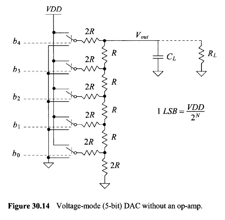
Desinging 10-Bit DAC using N-well Resistor of 10k
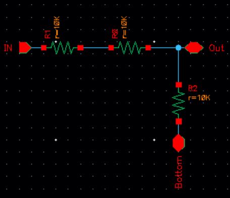
We
start our desing by first creating a voltage divider. This voltage
divider will make it easier to to creat our 10-Bit DAC. From this
voltage divider we will create a symbol. I have labeled the right node
as IN, the left node as OUT and the Bottom node as Botttom.
After
creating the voltage divider we will now creat our symbol. To creat a
symbol we do the following, we click creat, Cellview, and finally From
Cellview.
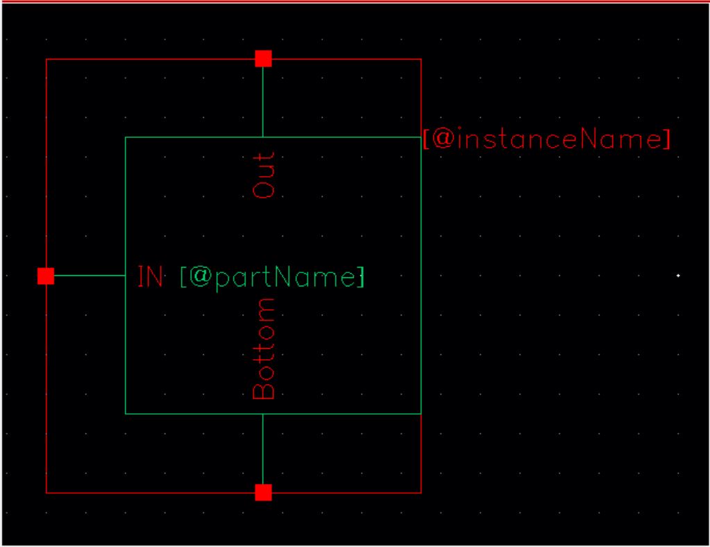
Once
the symbol was created edited as needed. After saving my progress I
countinued to make the 10-Bit DAC using the symbol from above.
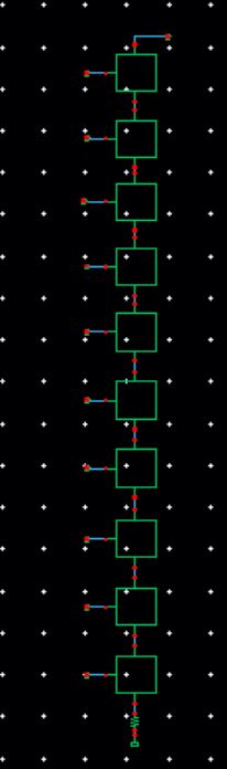
After
connecting all symbols together and adding a 10k resistor at the bottom
I created a new DAC symbol. We were to copy the symbol from the
directory, ideal 10-bit DAC to our folder and edit the symbol as needed.
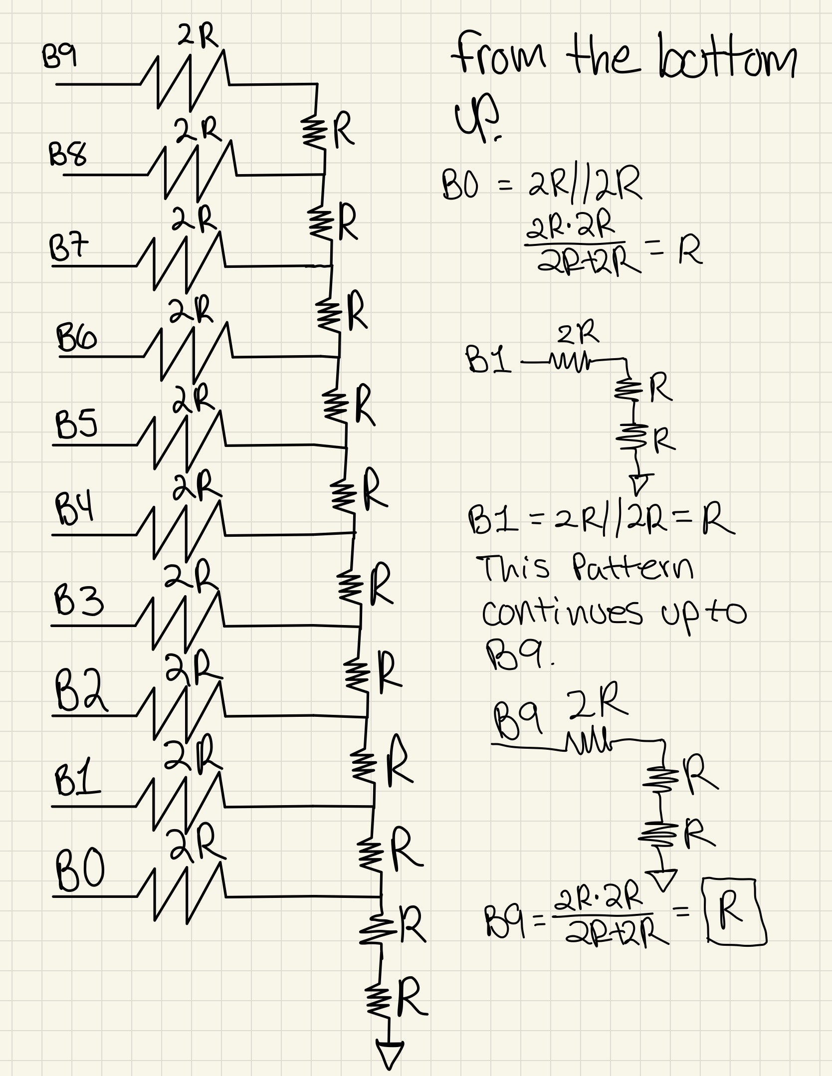
Calculating Output Resistance
Starting
from the bottom up we will work our way up combining resistors in
series and parallel to give us Req and keep doing this process until B9
is reached.
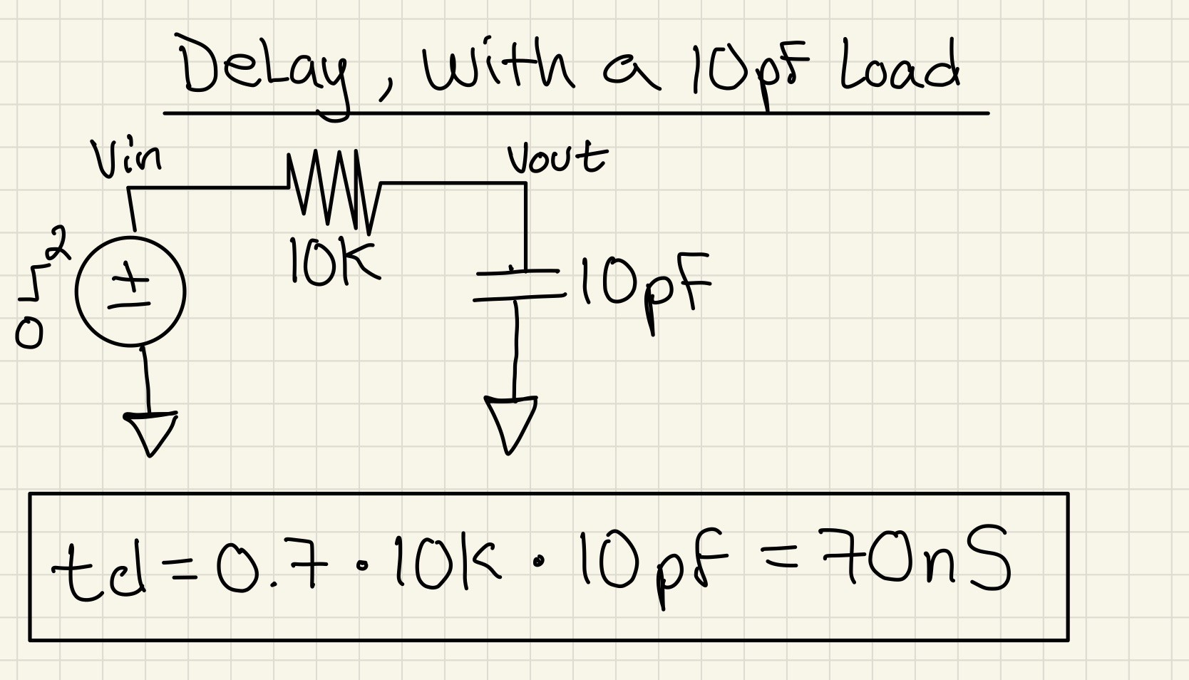
Calculating Delay with a 10pF load
This
circuit can be treat as and RC circuit since we have 10k resistor in
series with a 10pF capacitor. We know the time is around 0.7RC. The
following will show the hand calcs for our delay.
The
following will show my schematic and simulation of the delay. From the
calculation we esstimate the delay will be around 50% of the input.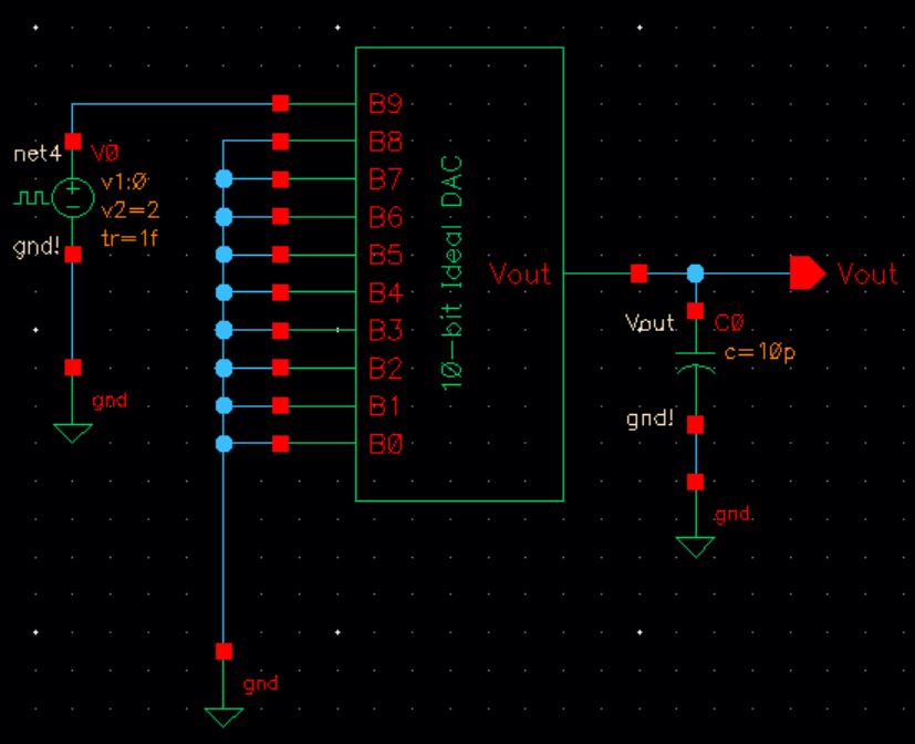
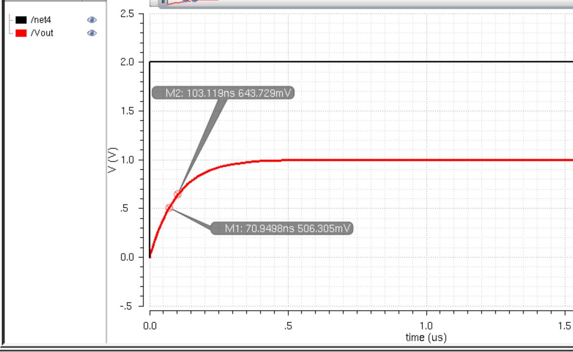
From the above simulaiton we can see the hand calcs were correct.
Testing our DAC design with no load
From the above simulation we can observe the same waveforms as the Ideal DAC from the prelab.
Testing our DAC design with 10k resistive load
From
connecting the load of 10k the circuit becomes a voltage divider which
will result in the ouput voltage being half the input. From the
above simulation we can correctly observe Vout going from 0 to 2.5v.
Testing our DAC design with 10pF load
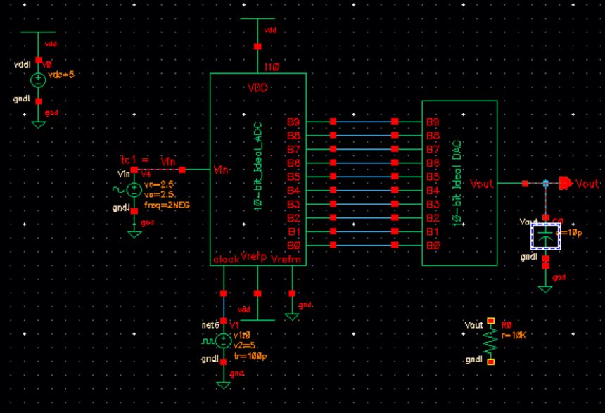
With the capacitor connected we observe a smooth curve which lags around 70ns.
Testing our DAC design with Resistor in parallel with Capacitor
From this simulation we can observe that with R//C we get Vout is half the input while also lagging roughly 50 ns.
Conclusion
From
the above simulation we can conclude that our 10-Bit DAC was
functional. We can also observe from the above simulations that when
there is no capacitive load our results will be in phase, but if a
resistive load is added we will experience a voltage divider, but still
in phase. When resistive load and a capacitive load is used the output
will lag the input. Finally when only using a capacitive load the
output will lag the input at a greater time.
Questions
- In a real circuit the switches seen above (the outputs of the ADC) are implemented with transistors (MOSFETs).
- Discuss what happens if the resistance of the switches isn't small compared to R.
In
a real circuit if the switch resistance was not samll compared to R,
the equivalent resistance of the DAC would not be R. The switch
resistance would be in series with R. To find this out we would have to
recalculate the R value for all of DAC to be able to maximize ouput.
Addtional information
- If you have simulation convergence problems you can force the simulation to converge by going to, in the ADE, Simulation -> Options -> Analog
- Set the values as seen below
- relative tolerance, reltol, of 10% (= 1e-1)
- voltage absolute tolerance, vabstol, of 100 mV (= 1e-1)
- current absolute tolerance, iabstol, of 1 mA (= 1e-3)
I
ran into this problem and the simulation would only output half the
waveform after correcting the issue I was able to see the correct
waveforms plot.
Backing up Work
I backed up my work twice for this lab, once during pre-lab then after I finished the post-lab.
Return to Labs