EE 421 Flyback Switching Power Supply
The Flyback inverter is a device that is commonly used in consumer electronics to charge
devices in a safely manner by converting AC to DC voltage and maintain a low voltage.The
reason the flyback is a safe tool to charge electronics is because it has two separate grounds one
related to the AC voltage and one tied to the DC voltage since the DC side is at a low voltage if
something were to happen one would not got get shocked as there is a small amount of current in
the DC side. The flyback inverter uses a mosfet as a switch to regulate the output voltage. The
switching of voltages is facilitated by using a transformer that rectifies the AC to DC voltage.
The output of my circuit will be 12.5V and be able to supply well beyond 2A of current to a load.
The device will be charging when the voltages surpasses 12.5V.
The device is activated when the mosfet turns on. when the mosfet is turned on the device drives a current through the the transformer to ground. In our design the transformer is an inductor. when the current gets pulled to gourd the right side of the inductor(L1) gets magnetized. When the mosfet shuts off all the current in the inductor is then transferred to the the right side of the inductor(L2). With all the current now on the right side of the transformer our reverse biased diode gets turned on and allows the current Id to flow to Vout. Following Will show my design schematic layout and results of the project.
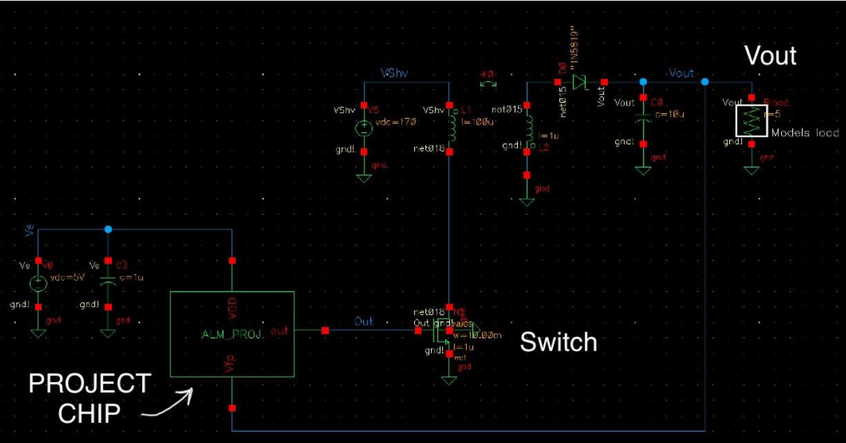
Project schematic with project chip.
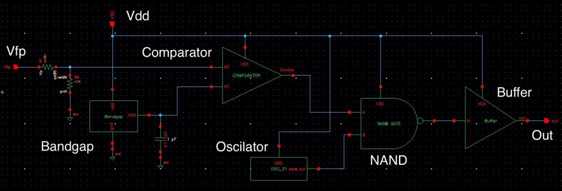
High level view of symbols for project design
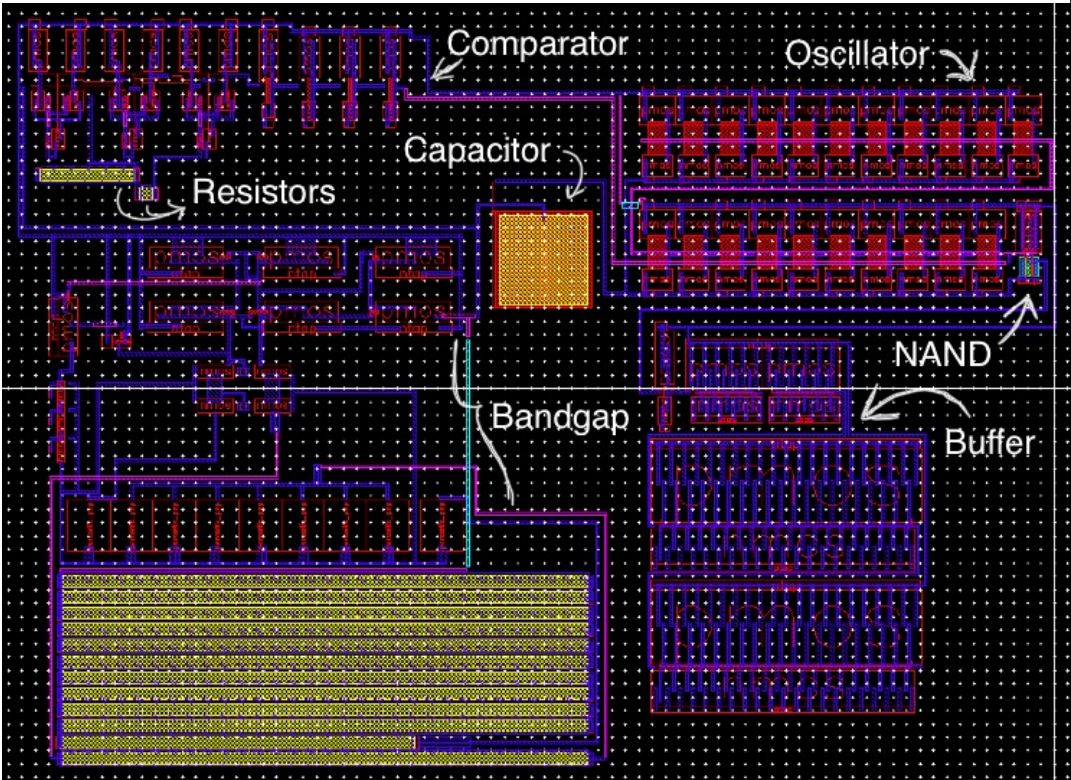
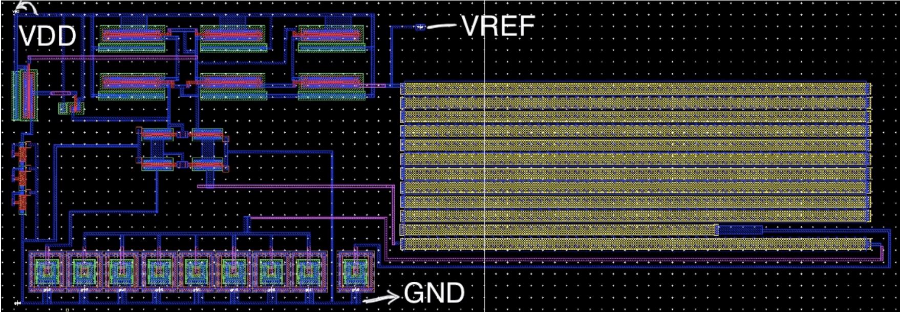
COMPLETE PROJECT LAYOUT
Results:
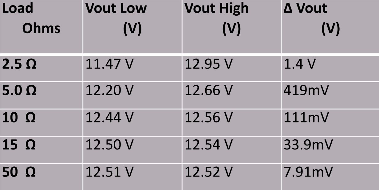
Results for Varying loads From all the varying results I believe my design works best at 10ohms.
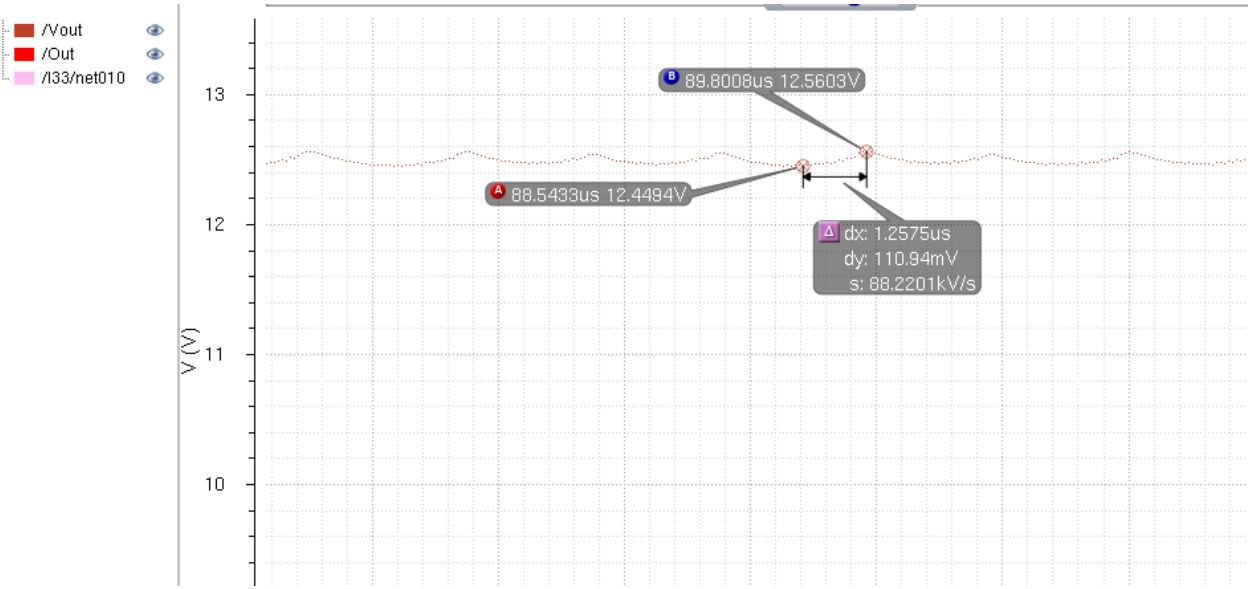
Simulation of Vout at 10ohms:
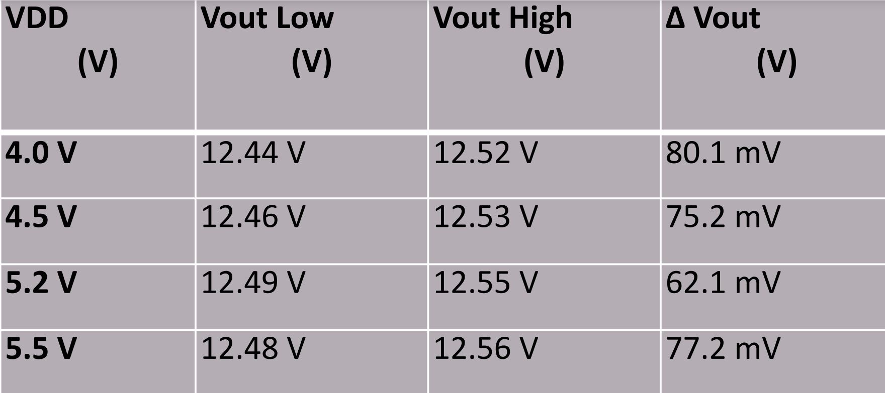
Results of varying VDD With a set load of 10 ohms
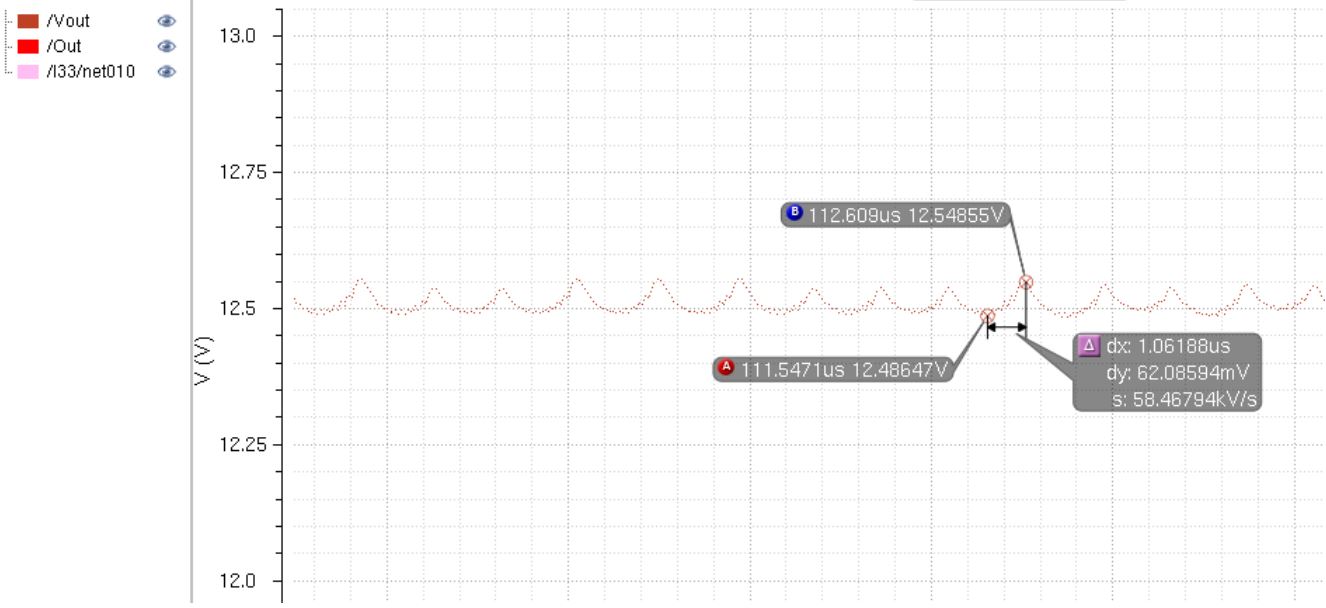
Simulation with VDD at 5.2V
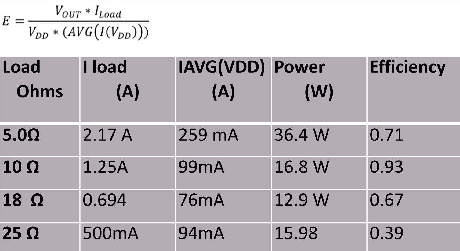
Power and Efficiency Results
used the following formula to calculate Efficiency
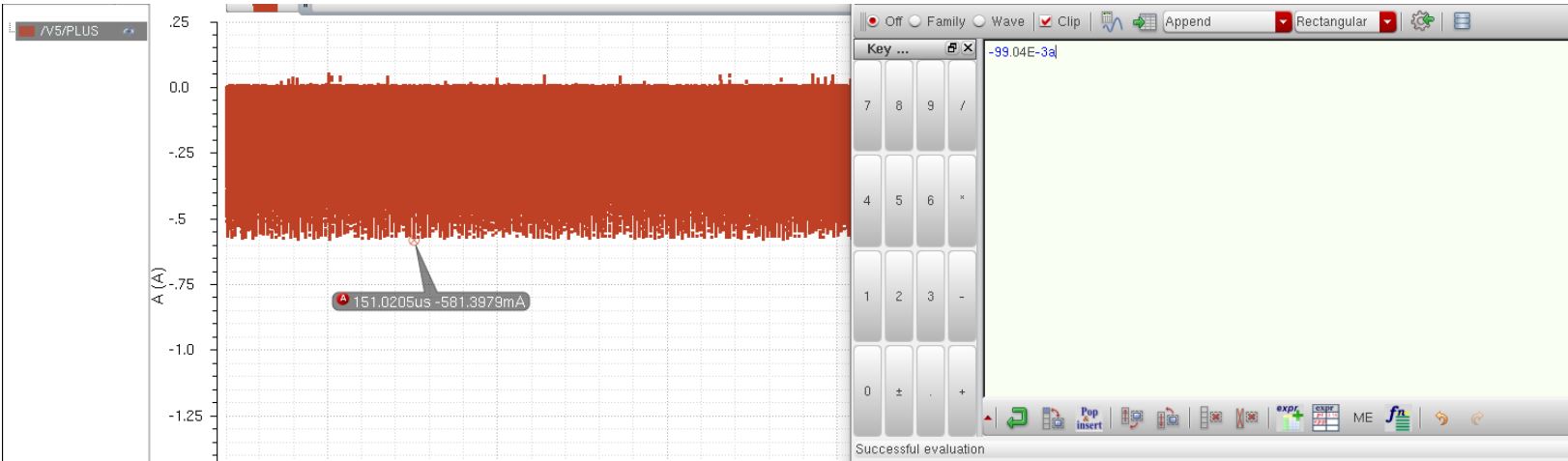
Cadence calculator used to calculate avg current at I(vdd) & I(load)
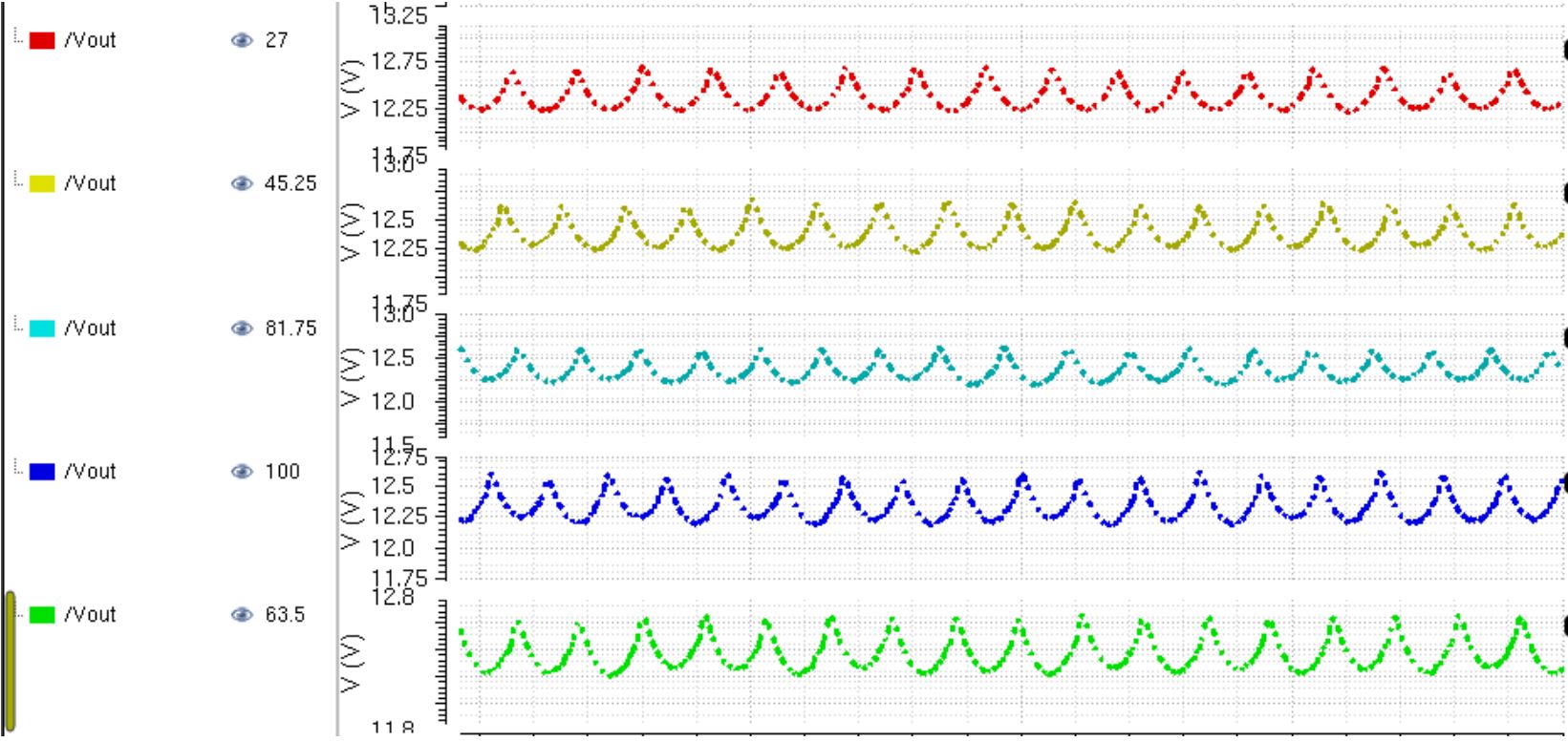
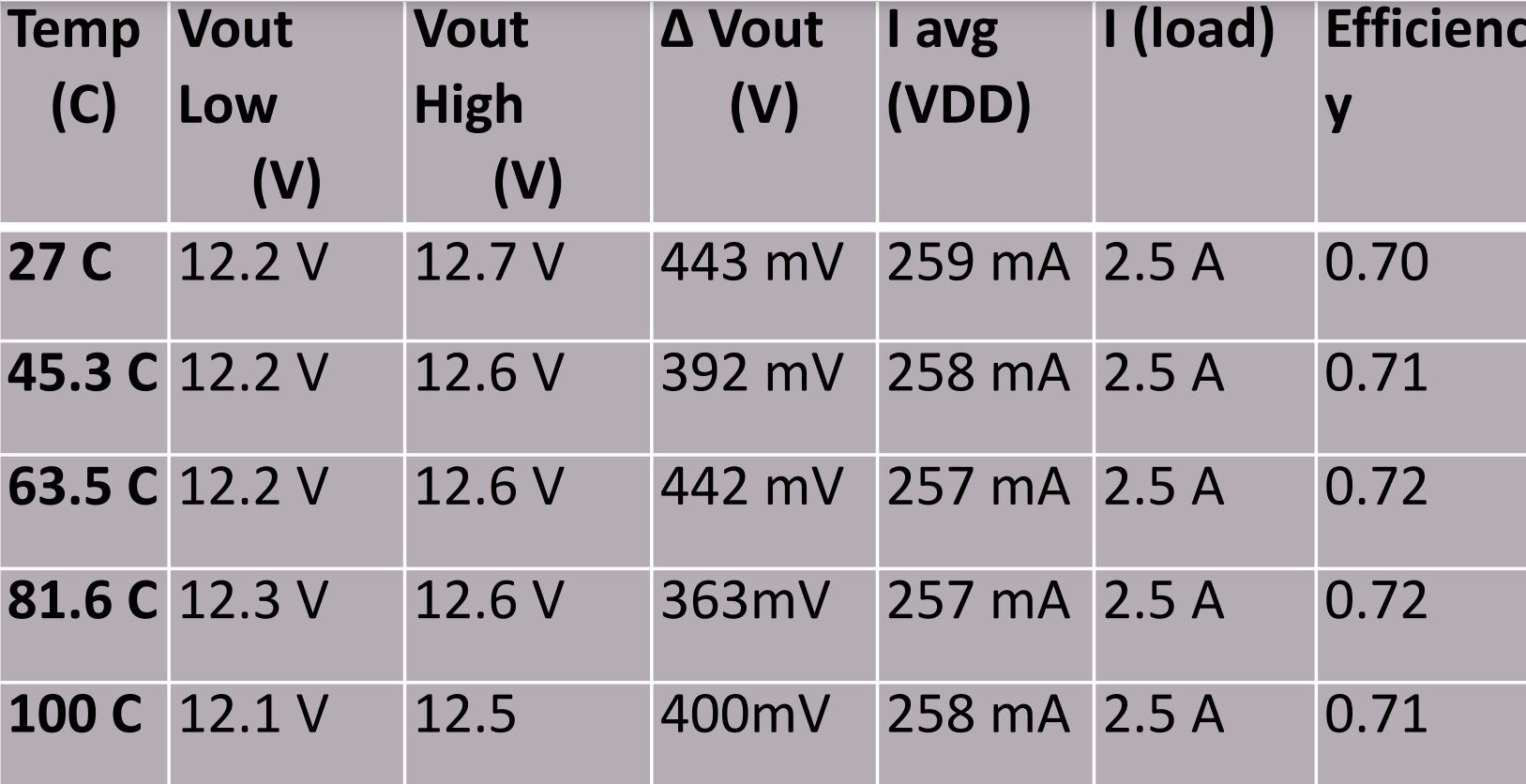
Varying Temp Simulations
Next I will show each part of my chip individually and explain how it works in the over all design.
PROJECT DESING
✴Band Gap - Is our reference circuit that will output a constant voltage.
✴Buffer - Is used for delay and to filter out the noise
✴oscillator - The oscillator is used to control the cycles and frequency of the circuit’s operation.
✴Comparator - The comparator takes in two inputs, and depending on which input is greater the output will be VDD or ground.
Diode simulation for increasing temperature in the bandgap
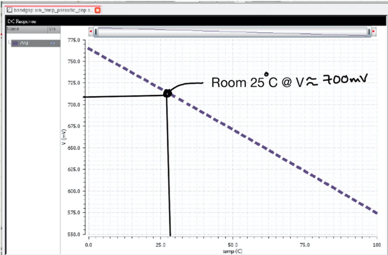
In this simulation we can observe the change in a diode internal voltage as temperature changes from 0 to 100 Celsius. At room temperature roughly 25 C. we know the diodes internal voltage is 0.7V. From the simulation can observe that as temperature increases the internal voltage of the diode decreases. This means when operating at higher temperatures it would take less potential to have the diode in forward bias. As temperature decreases the internal voltage increases needing a higher potential to have the diode in forward bias.
Simulation for increasing temperature in the bandgap
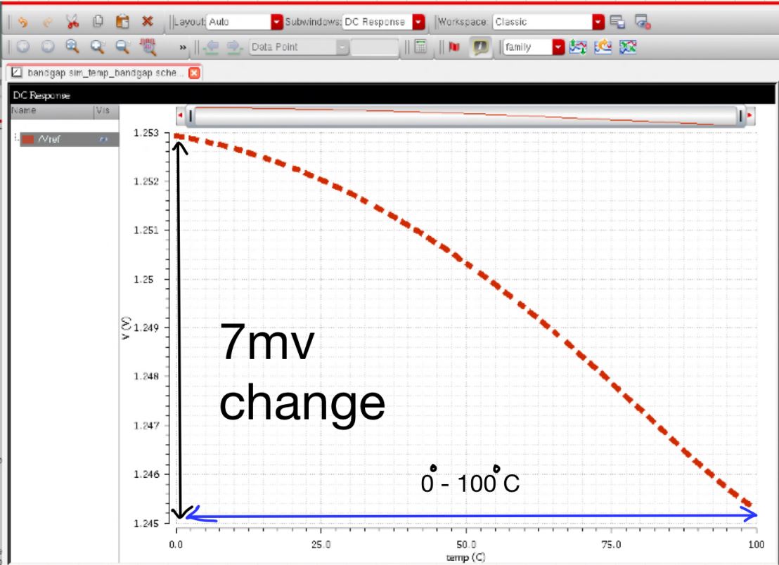
This simulation we observe Vref aginst temperature (C ). We can observe that Vref has a small change of roughly 7mv as the temperature goes from 0 to 100 Celsius. From this we can conclude that temperatures from 0 to 100 has small effects on the bandgap.
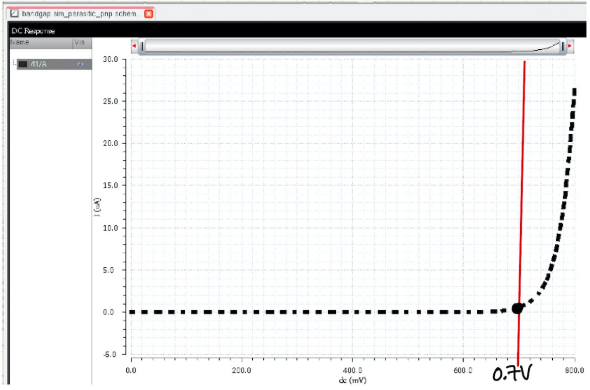
simulation for diode potential
This simulations shows how the Pn Junction diode turns on and starts to conduct current. A diodes Internal Voltage has to reach 0.7V to start conducting current. The following simulations proves that as the diode turns on roughly around 0.7V.
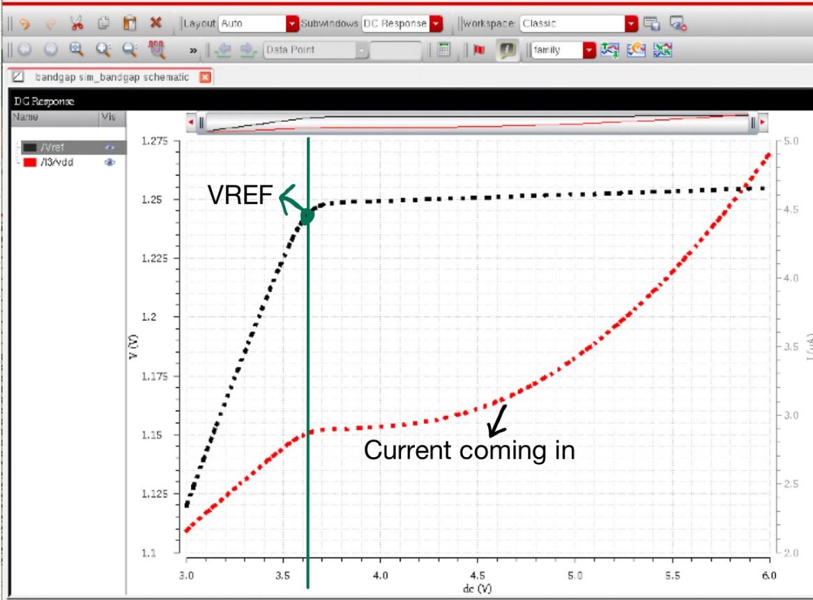
Simulation for increasing VDD in the bandgap
For this simulation we can observe that once the voltage on VDD raises too about 3.7V Vref Maintains almost a steady voltage of around 1.25V. This means that as VDD and the current increases it does not effect Vref.
Layout of the Bandgap: circuit passes both DRC & LVS rules.
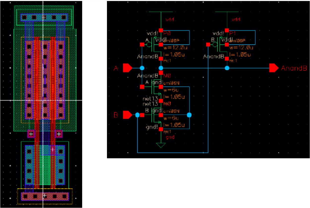
Schematic and layout of NAND Gate: The design passes both DRC & LVS rules.
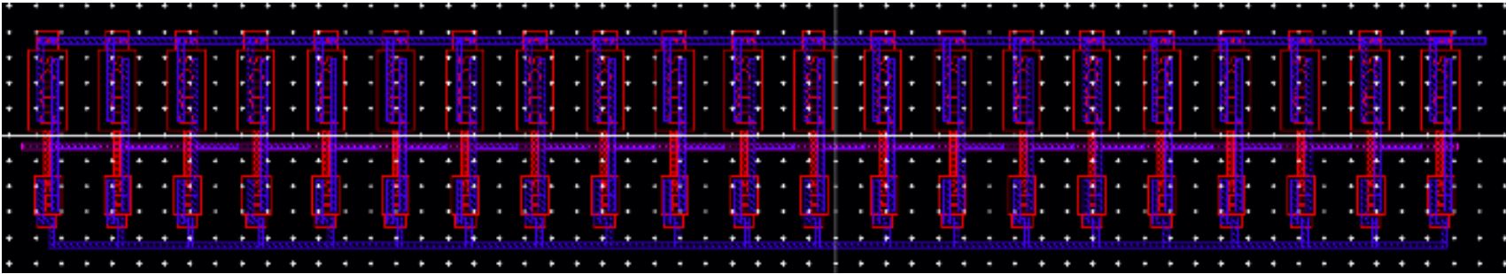
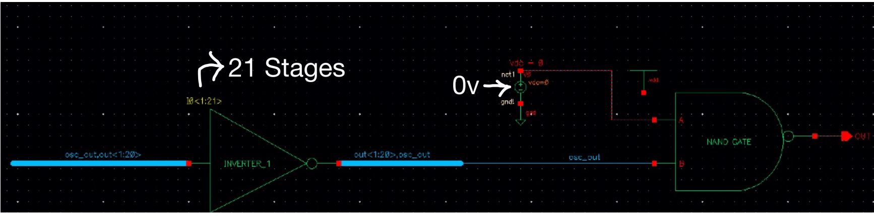
layout of Ring Oscillator:
Design passes DRC & LVS rules. For my design I decided to use 21 stages for the ring oscillator.

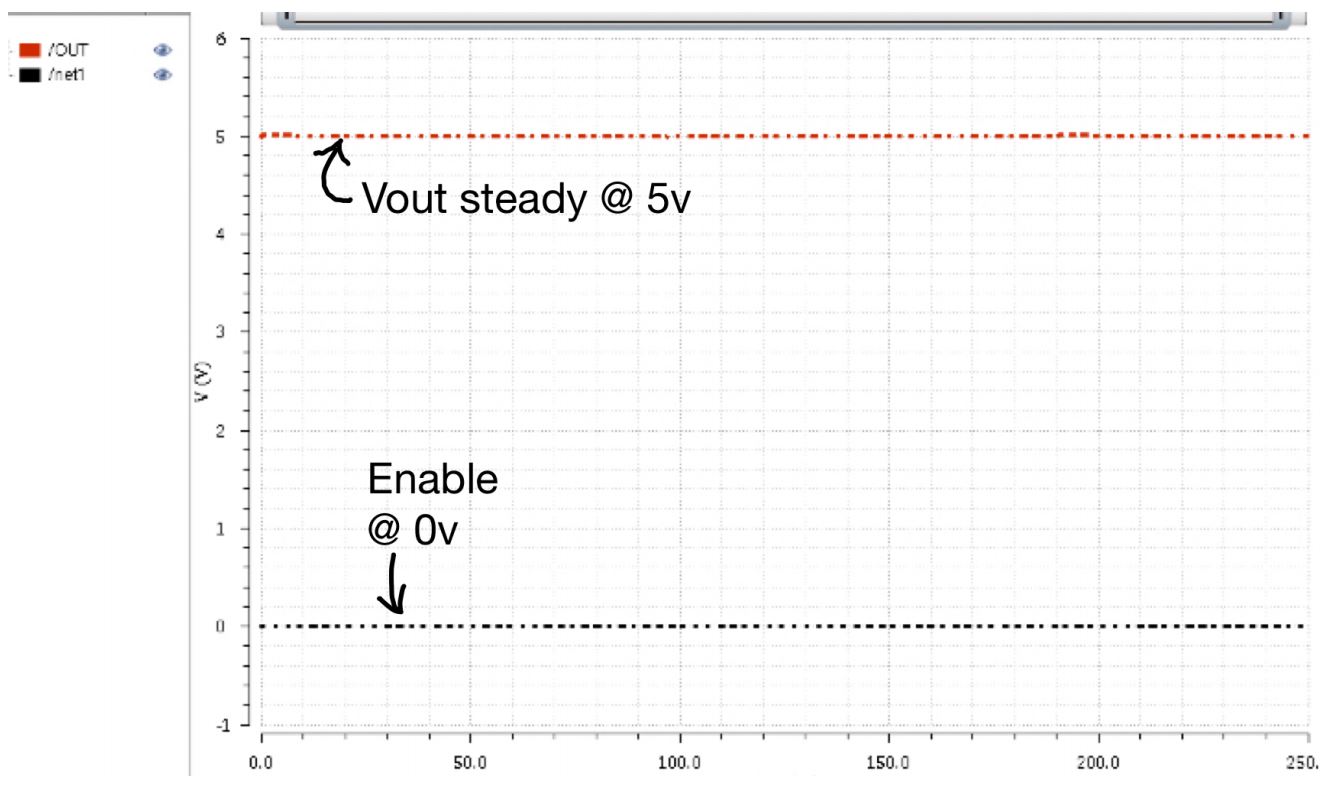
Simmulation of Ring Oscillator with NAND gate:
For our design the oscillator should be right around 5MHz
Hand calculations to estimate number of stages for a desired frequency ended up using more stages than calculated for, But obtained the desired frequency

When enable from the comparator is at 5v we expect the output to act as the oscillator.
When enable come from the comparator at 0v we expect the output to be steady at 5v.
Oscilator schematic, layout, and simulation: Device also passes DRC & LVS rules.
Comparator Simulation:
Showing output before the inverters and after with a visibly cleaner logic signal. It should be noted that proper comparator operation can also be viewed here as the sensing voltage drops below bandgap voltage the device outputs a clean logic 1 enable signal and 0 when voltage is above the 1.25V bandgap voltage as expected.
Buffer Simulation:
Showing buffer transition time of approximately 1ns with 582ps delay
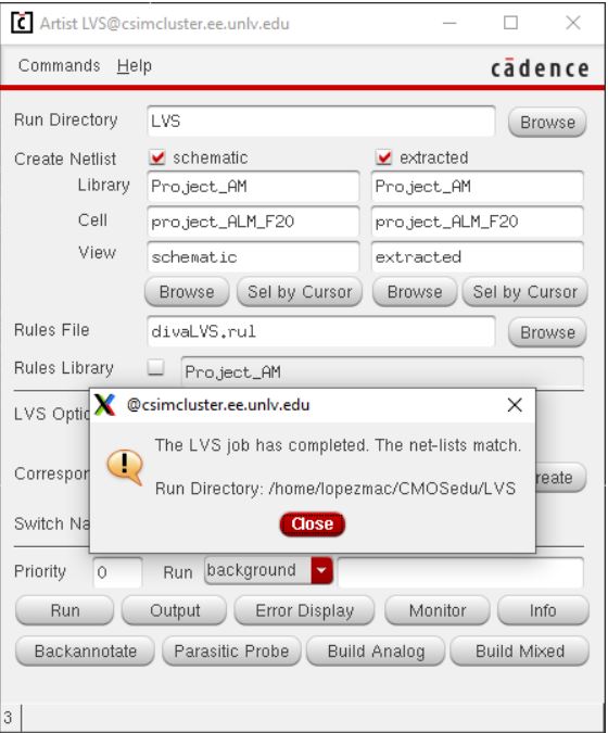
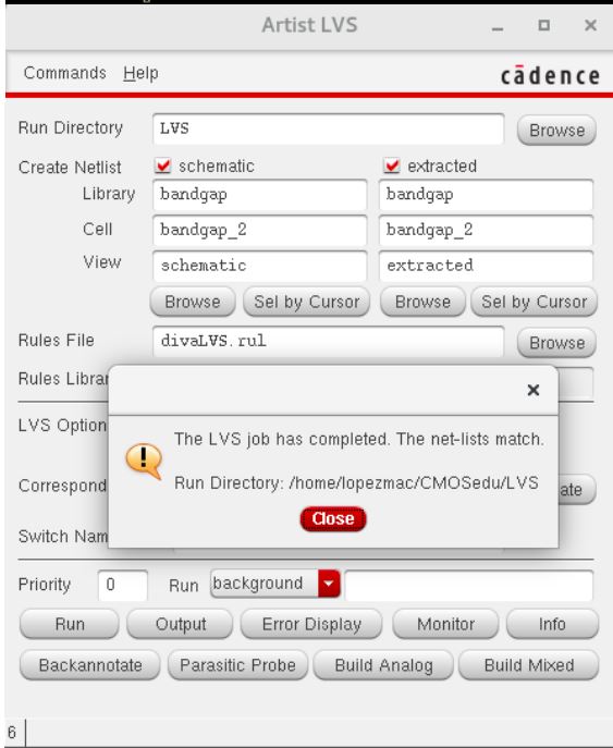
1. Issues LVSing
• I was having issues getting to understand how they layout and schematics match not only must they be the same but names, wire labels, and nodes matter when it comes to LVS.
• Found the most useful solution to this was reading the output report when netlist did not match.
• learned that if you select error display while in the extracted mode of the LVS the program highlights the area of issue in both the extracted and schematic
2. Oscillator
• Found more stages made it easier to achieve the desired delay and frequency, but at the cost of having a large Layout.
• lower number of stages with weak inverters also lead to a higher power consumption
3. Buffer
• The same issue as the oscillator but also had to play around more with the sizes and ratios of the NMOS and Pmos.
• Form this design I found it easier to include smaller widths and larger number of multipliers. easier in the sense of connection in the layout.
• had issues understanding how the multipliers connected in the layout at first.
4. Comparator
• issues working out pros and cons of the transistors sizes.
• notices that smaller devices had less power consumption but had longer delays.
Return to Homepage
The device is activated when the mosfet turns on. when the mosfet is turned on the device drives a current through the the transformer to ground. In our design the transformer is an inductor. when the current gets pulled to gourd the right side of the inductor(L1) gets magnetized. When the mosfet shuts off all the current in the inductor is then transferred to the the right side of the inductor(L2). With all the current now on the right side of the transformer our reverse biased diode gets turned on and allows the current Id to flow to Vout. Following Will show my design schematic layout and results of the project.
Project schematic with project chip.
High level view of symbols for project design
COMPLETE PROJECT LAYOUT
Results:
Results for Varying loads From all the varying results I believe my design works best at 10ohms.
Simulation of Vout at 10ohms:
Results of varying VDD With a set load of 10 ohms
Simulation with VDD at 5.2V
Power and Efficiency Results
used the following formula to calculate Efficiency
Cadence calculator used to calculate avg current at I(vdd) & I(load)
Varying Temp Simulations
Next I will show each part of my chip individually and explain how it works in the over all design.
PROJECT DESING
✴Band Gap - Is our reference circuit that will output a constant voltage.
✴Buffer - Is used for delay and to filter out the noise
✴oscillator - The oscillator is used to control the cycles and frequency of the circuit’s operation.
✴Comparator - The comparator takes in two inputs, and depending on which input is greater the output will be VDD or ground.
Bandgap
The Bandage is a voltage reference circuit that outputs a constant voltage independent of the
power supply. The bandage circuit will be used in the flyback inverter to give us a reference
voltage (Vref) of 12.5v. Vref in then will be used to signal the comparator to turn on or off. The
following will show how the bandgap simulations work.Diode simulation for increasing temperature in the bandgap
In this simulation we can observe the change in a diode internal voltage as temperature changes from 0 to 100 Celsius. At room temperature roughly 25 C. we know the diodes internal voltage is 0.7V. From the simulation can observe that as temperature increases the internal voltage of the diode decreases. This means when operating at higher temperatures it would take less potential to have the diode in forward bias. As temperature decreases the internal voltage increases needing a higher potential to have the diode in forward bias.
Simulation for increasing temperature in the bandgap
This simulation we observe Vref aginst temperature (C ). We can observe that Vref has a small change of roughly 7mv as the temperature goes from 0 to 100 Celsius. From this we can conclude that temperatures from 0 to 100 has small effects on the bandgap.
simulation for diode potential
This simulations shows how the Pn Junction diode turns on and starts to conduct current. A diodes Internal Voltage has to reach 0.7V to start conducting current. The following simulations proves that as the diode turns on roughly around 0.7V.
Simulation for increasing VDD in the bandgap
For this simulation we can observe that once the voltage on VDD raises too about 3.7V Vref Maintains almost a steady voltage of around 1.25V. This means that as VDD and the current increases it does not effect Vref.
Layout of the Bandgap: circuit passes both DRC & LVS rules.
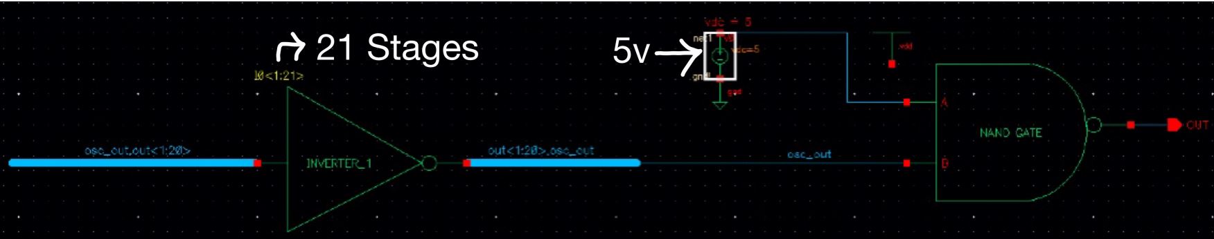
NAND Gate & Ring oscillator
The oscillator in the Flyback inverter will be used to control the cycle and frequency of the
circuit’s operation. The ring oscillator is made up of weak inverters controlled by a NAND gate.
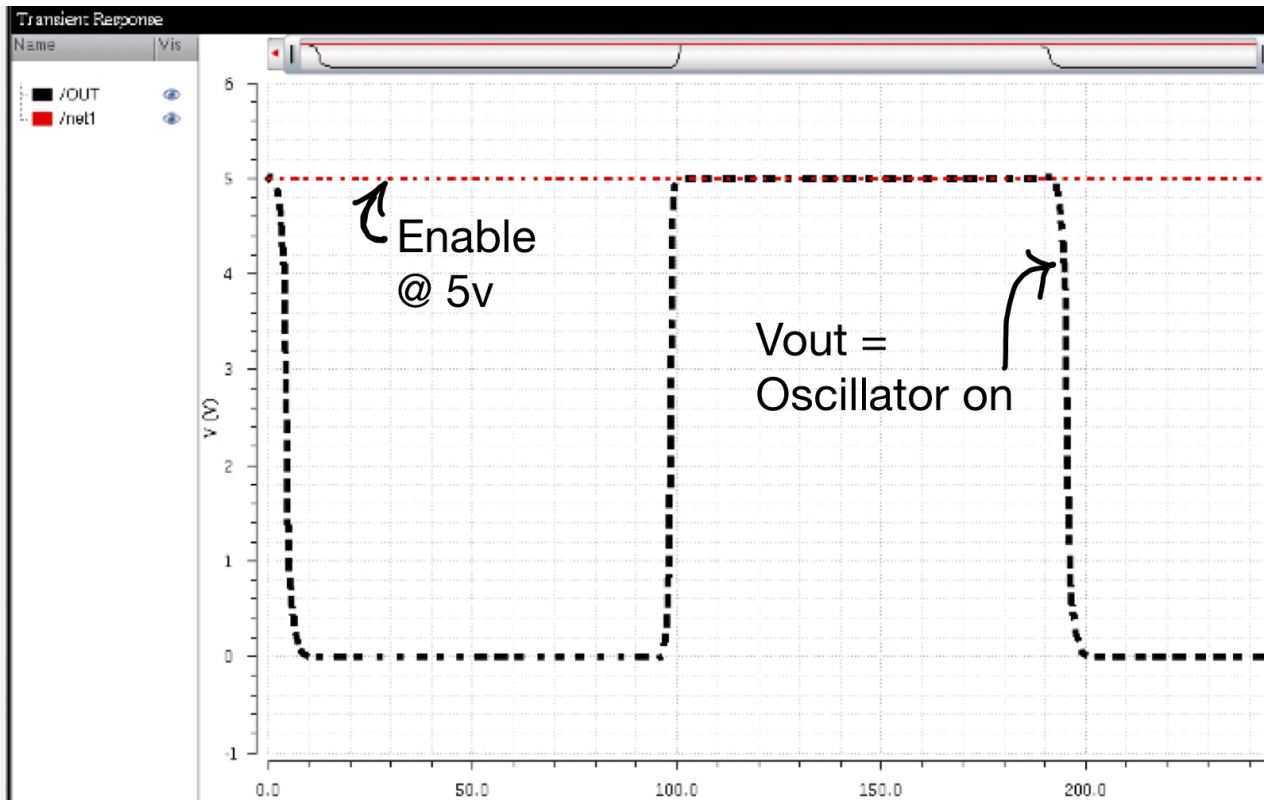
The NAND gate takes in the Enable output signal from the comparator and the output of the ring
oscillator as the inputs. When the enable signal comes in at 5v the NAND gates treats it as a
logic 1. When the Enable signal comes in at 0v the NAND gate treats it as a logic 0. When the
enable is 5v the output of the NAND gate acts like the oscillator. When the enable is 0v the
output of the NAND gate is steady at 5v. Schematic and layout of NAND Gate: The design passes both DRC & LVS rules.
layout of Ring Oscillator:
Design passes DRC & LVS rules. For my design I decided to use 21 stages for the ring oscillator.
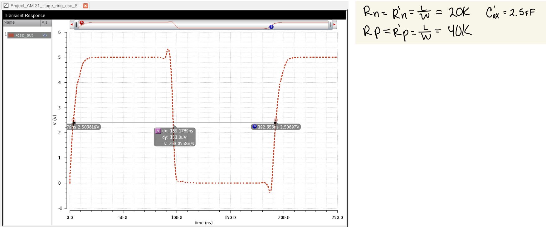
Simmulation of Ring Oscillator with NAND gate:
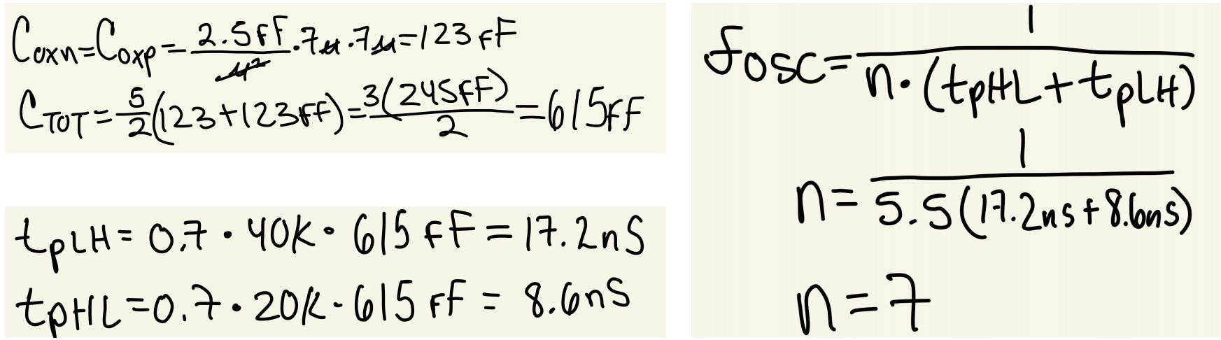
For our design the oscillator should be right around 5MHz
Hand calculations to estimate number of stages for a desired frequency ended up using more stages than calculated for, But obtained the desired frequency
When enable from the comparator is at 5v we expect the output to act as the oscillator.
When enable come from the comparator at 0v we expect the output to be steady at 5v.
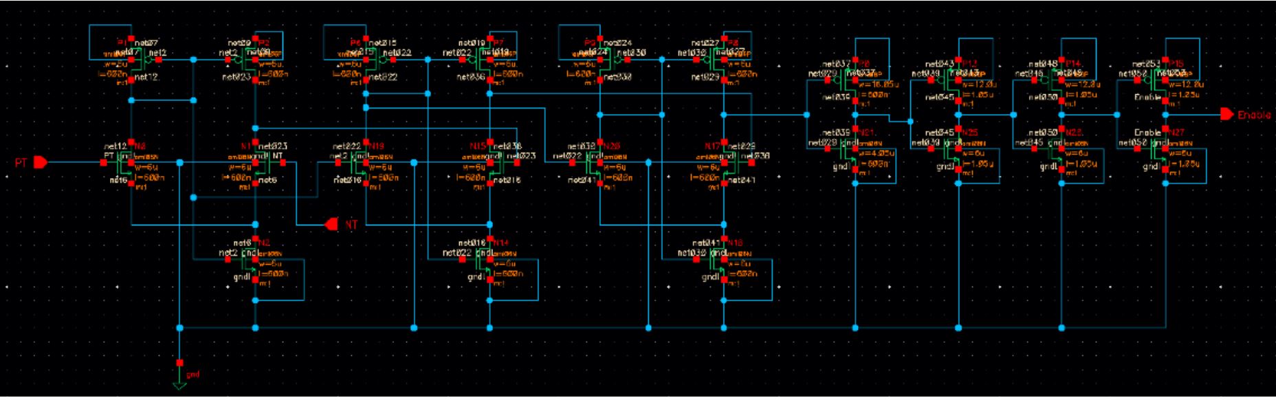
The Comparator
In the flyback inverter the comparator is what acts a sensor to either turn on and charge the
device or shut the device off when its fully charged. The comparator works by comparing two
terminals the positive and negative terminal. When the positive terminal is High the output acts
as a logic 1 and when the negative terminal is High the outputs acts as logic 0. These signals will
be sent to the ring oscillator and NAND gate to turn on and off the device.Oscilator schematic, layout, and simulation: Device also passes DRC & LVS rules.
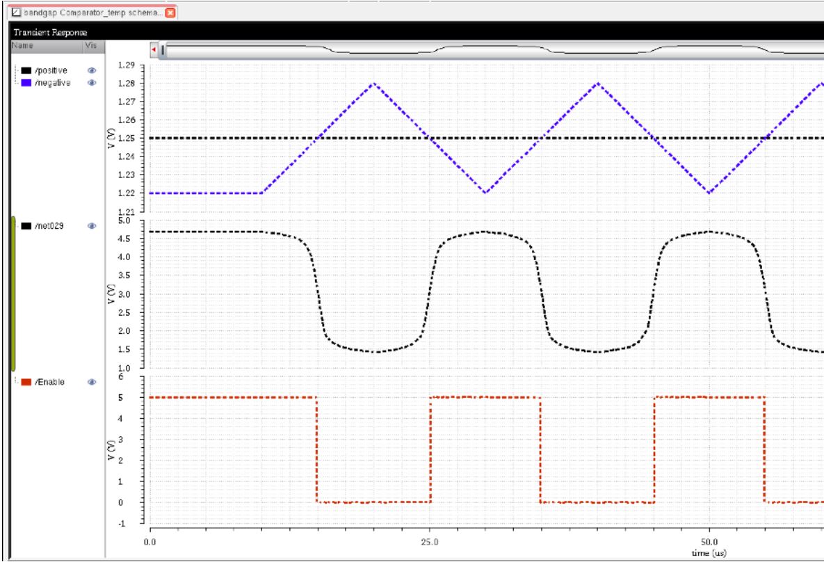
Comparator Simulation:
Showing output before the inverters and after with a visibly cleaner logic signal. It should be noted that proper comparator operation can also be viewed here as the sensing voltage drops below bandgap voltage the device outputs a clean logic 1 enable signal and 0 when voltage is above the 1.25V bandgap voltage as expected.
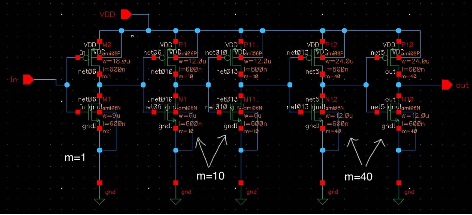
The Buffer
The buffer in the design is used to drive the NMOS which acts as a switch. The buffer has to
have a low switching point in order to be effective.
For the buffer I used a stage of 18u/9u with a Multiplier of 1, a stage of 12u/6u with a multiplier
of 10, and lastly a stage with 24u/12u with a multiplier of 40.
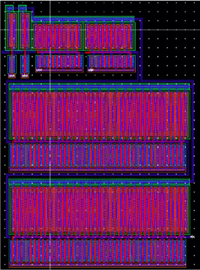
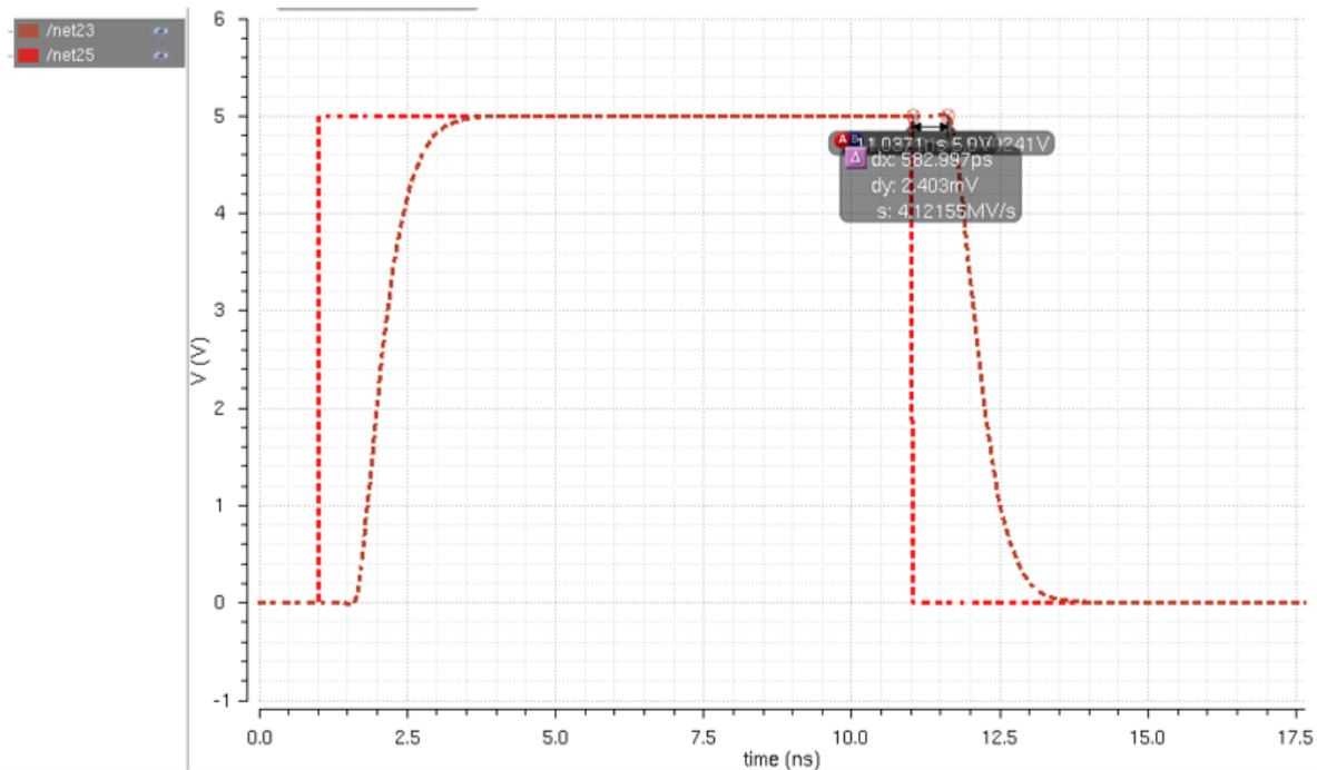
The design both passes DRC & LVS.Buffer Simulation:
Showing buffer transition time of approximately 1ns with 582ps delay
Conclusion
This was the first project I have done with power supply and also the first project I have done
that I understood what was going from beginning to end. Although I had hardships I was able to
over come them with the understanding of how each of the components works. following is some
of the issues I encountered while doing the project.1. Issues LVSing
• I was having issues getting to understand how they layout and schematics match not only must they be the same but names, wire labels, and nodes matter when it comes to LVS.
• Found the most useful solution to this was reading the output report when netlist did not match.
• learned that if you select error display while in the extracted mode of the LVS the program highlights the area of issue in both the extracted and schematic
2. Oscillator
• Found more stages made it easier to achieve the desired delay and frequency, but at the cost of having a large Layout.
• lower number of stages with weak inverters also lead to a higher power consumption
3. Buffer
• The same issue as the oscillator but also had to play around more with the sizes and ratios of the NMOS and Pmos.
• Form this design I found it easier to include smaller widths and larger number of multipliers. easier in the sense of connection in the layout.
• had issues understanding how the multipliers connected in the layout at first.
4. Comparator
• issues working out pros and cons of the transistors sizes.
• notices that smaller devices had less power consumption but had longer delays.
Return to Homepage