Final Project: 32 Word 8 Bit Register File - ECE 421L
Authored
by Luis Garcia Rivas
garciari@unlv.nevada.edu
November 24, 2021
Final Project Description
For
the lab final project I was tasked with designing a Register File that
handles 32 words each consisting of 8 bits of data.
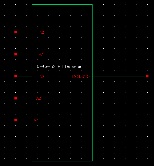
To address all of the 32 words I will have to implement 5 address inputs (2^5 = 32 words). For the 8 bits of data I had to add
8
datalines. The unique thing about the datalines is they would function
as inputs and outputs. To control when they're inputs(write)
and when they're outputs(read) I used an nmos with the gate input connected to my R_WI(Read_WriteComplement) control signal
that
will connect a voltage source to the dataline if R_WI was set to write
and not connect the data source to the dataline if the
gate input was connected set to read mode. With the description of what I was tasked to create out of the way I can now show you
my final project design process, explaination, designs, and simulations
Part 1: Schematics and Design Discussion
For
part 1 of the lab I was tasked with creating a working schematic of my
32 word 8 bit register file. As well as explaining all of my
design
descions. For my design I decided(along with strong recommendation from
Dr.Baker) to break up my RF into modules so that I can
test
each part indivdually and save myself headaches. The design order for
my project is SRAM Inverter -> Inverter(12u/6u) -> 1 Bit SRAM Cell
-> NAND5 -> Decoder -> Register File.
| 1 | SRAM Inverter
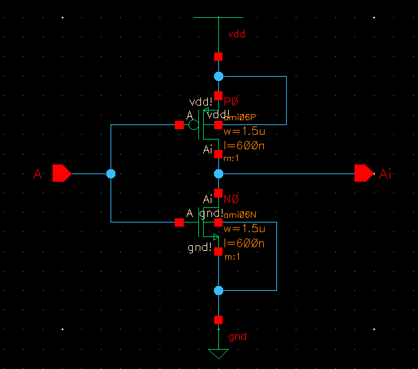
Why do I have 2 different types of inverters?
The
reason behind having to different types of inverters is that for my
SRAM Inverter(pictured above) I want to have week inverters so that in
the sram cell the cross coupled inverters are quickly chainging values
with minimal delay. Thus we can reduce errors in which we sample the
data in the cell for reading when it is a non valid logic voltage.
Now
that we know the reason for 2 different types of inverters in my design
I can now explain the SRAM inverter. As stated above we want to create
weak inverters for the cross coupled inverters within our SRAM cell
thus I went with minimum width of 1.5u. The schematic above is a basic
inverter consisting of a pmos tied to VDD and a nmos tied to gnd with
both gate inputs tied to an input A and producing an output of Ai(A
inverted). I believe this design is great for my use case due to
the fact that I tackled the biggest issue which is making sure that the
inverter is weak. Possible improvements for this design is to find
sizing that will be more adaptable to different frequencies. However
since we were told not to worry about speed in our design this design
should suffice.
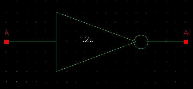
Symbol
 |
| 2 | 12u/6u Inverter
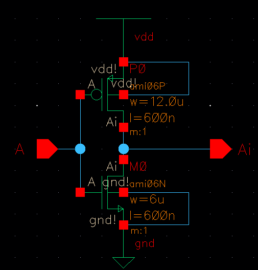
As
explained above I needed a separate SRAM inverter for the purpose of
being weak so that it can be bullied. Thus I have this inverter which
is used in the NAND and decoder. Since speed isn't a concern I dedcided
to go with 12u/6u inverter since its reliable, thus reducing the
possiblities of errors. Improvements could be made in the design to
make it more compatible with different frequencies.
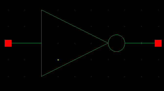
Symbol
 |
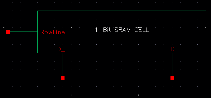
| 3 | 1 Bit SRAM Cell
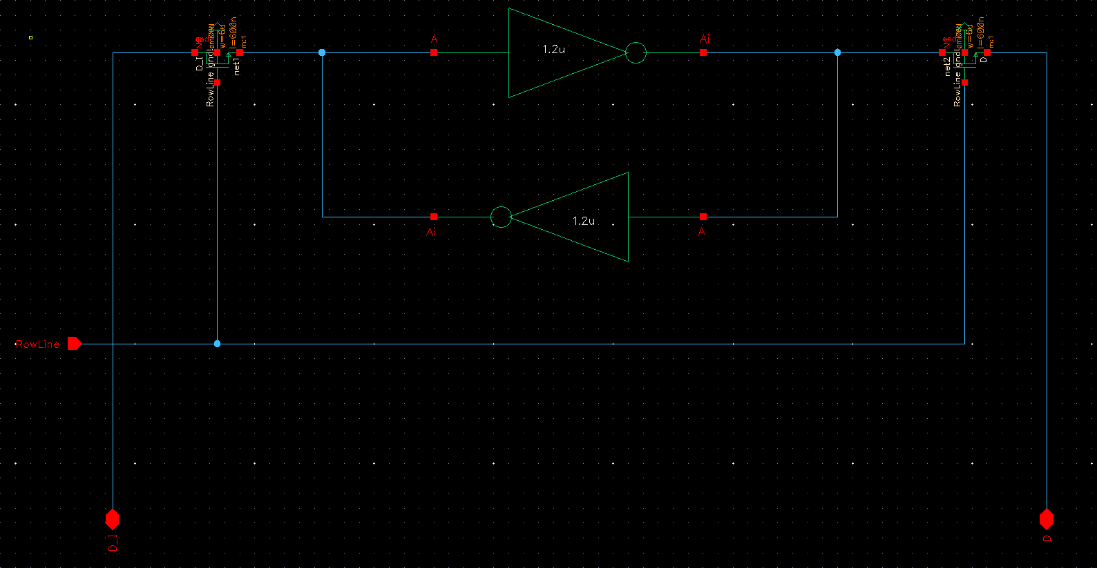
My
sram cell consists of 2 of the SRAM inverters cross coupled, 2 control
NMOS, a rowline input, and 2 Data inputs(complements of each other).
The SRAM cell stores a value and is stored by inverters which is
great since it reduces the need to be refreshed however it is volatile
thus our data disappears once power is gone. The rowline input is
controlled by the row decoder. If we input an address then the
appropriate rowline goes HIGH and every bit connected to that rowline
has their nmos's turned on. The D input/outputs either sample the data
being stored in the the SRAM cell or writes new data to the cell. This
again depends on what mode we're in. For my design I dediced to the
place the inversion of D data line outside of the sram cell to save my
self the trouble of having to instantiate an inverter for each sram bit
cell. I itered this sram cell 8 times per word since each word supposed to have 8 bits of data.
Symbol
 |
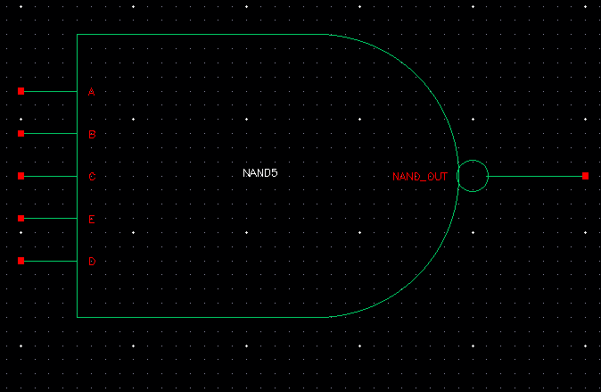
| 4 | Nand 5
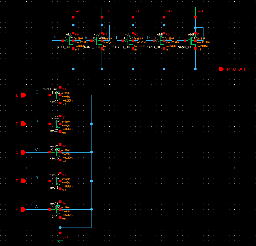
The
next module that needed to be designed is a 5 input NAND gate. This is
the heart of my row decoder. The 5 input NAND gate takes in 5 inputs
which pertain to our 5 bit address and outputs 0 if it is true. For my
5 input NAND gate I dedcided to once again go with 6u NMOS and 12u PMOS
to ensure uniformity across my entire design outside of the SRAM bit.
With this uniformity I should be able to reduce the amount of errors
with timings.
Symbol
 |
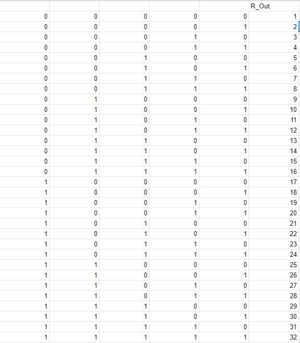
| 5 | Row Decoder
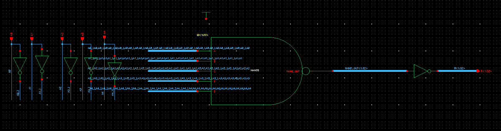
My
row decoder consists of a 5 input nand gate that takes in all 32
possible address bits then outputs a 32 0 representing a rowline to go
high then inverts this 0 to a 1 so that our rowline goes high. For
example if I input address bit 00000 then NAND_OUT<1> which is
low is fed through the inverter which turns it high and is then fed to
the SRAM cells in row 1. All other 32 cases turn out to be high since
its a nand gate and are then inverted low thus their cell bits do not
turn on. All of the inverters in this schematic are the 12u/6u inverter
again for uniformity across my design. As with other modules I would
probably improve this circuit by taking into account frequency to make
our schematic more compatible with other frequencies. A minor change I
would make is to figure out a more concise way of denoting the bus
lines so that I don't have 32 possible inputs per NAND gate as shown
above.
Symbol
Row Output Truth Table
 |
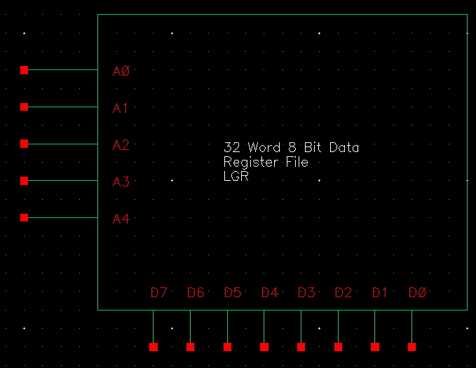
| 6 | Register File
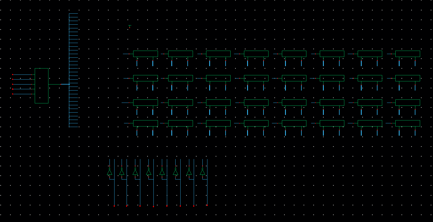
Finally
the register file. The register file is composed all previously
discussed modules put together to create my 32 word 8 bit data register
file. I instiated 32 8 instances of my sram cell so that each of the 32
words has 8 bits of data to output. Each of the SRAM cells above
represent a rowline with 8 cells attached to it. The row decoder
outputs the results of my 5 input NAND gate and feeds it to the
appropriate row. Thus if we input 10000 all other rows are low except
for row 17 which is high and feeds on data from our data lines or feeds
data out to our datalines. I have 8 datalines D0-D7 which feed into the
appropriate bit for all rowlines. The datalines are also connected to
inverters to feed its complement into the D_I input for all bits. With
all of the parts attached we now have a functioning register file that
allows for the input and output of 8 bits of data accross 32 locations.
The R_WI control signal is outside of the register file since otherwise
our D lines would only serve as inputs and not outputs due to a source
being connected directly to the input.
Symbol
 |
Part 2: Simulations
Simulation 1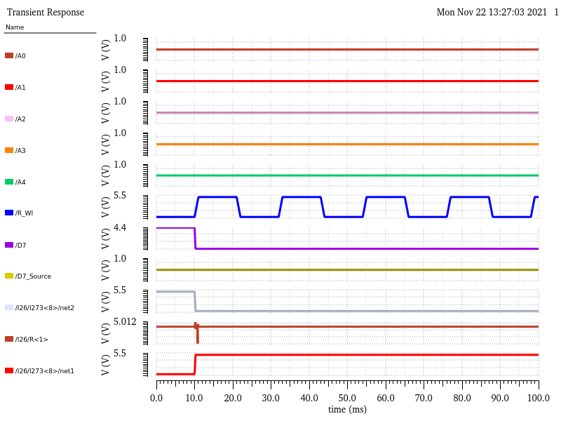
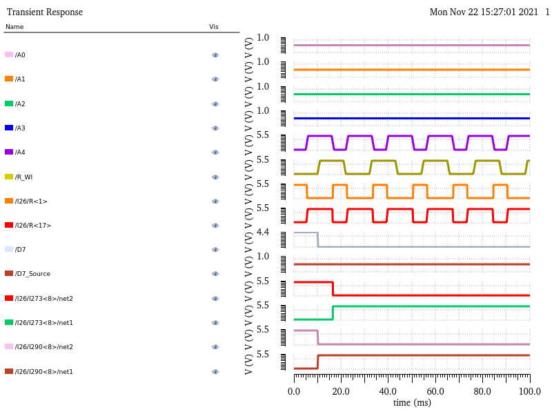
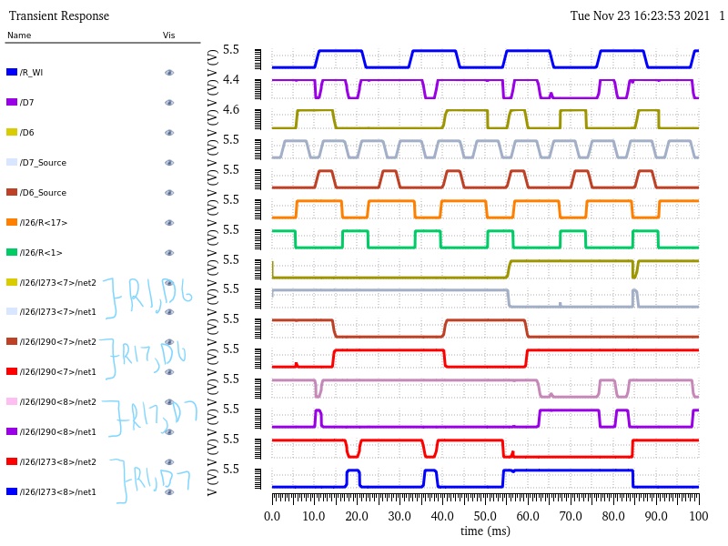
First
simulation testing static address, checking only 1 data bit(D7), net2
represents D side of sram cell, net 1 represents D_I side, D side
line
is precharged high. R<1> is our rowline for address 00000.
D7_Source represents what we want to write to our sram cell when the
R_WI
is
set to write mode. D7 represents what is currently going through D7
input/output which could be D7_Source or whatever is stored in our
SRAM
cell depending on what mode we're in. As we can see that with
precharged high sram and read mode our D7 is initially equal to our
sram cell however as we pulse to write mode it equals to D7_Source(0V).
Since we don't change our D7_Source for the rest of the time our D7 and
sram cell are set to 0v.
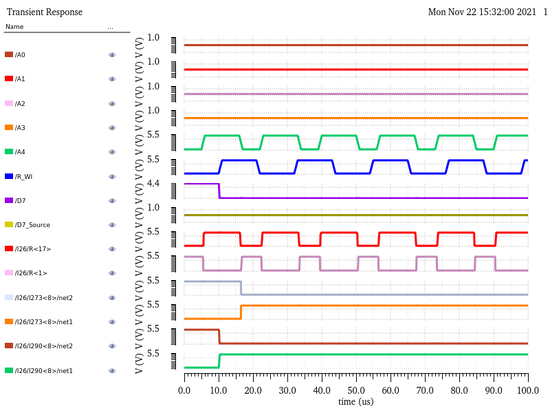
Same parameters as previous simulation however testing to see if any differences/errors occur when operating at microseconds.
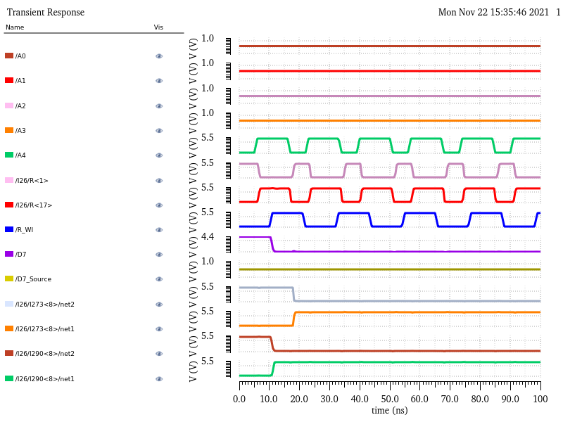
Same simulation as previous 2 however operating at nanoseconds to see if errors or differences occur. I
can see that there appears to be a more promient delay in my sram cell
when writing which could become a problem with a fast enough pulsing
data source.
Simulation 2
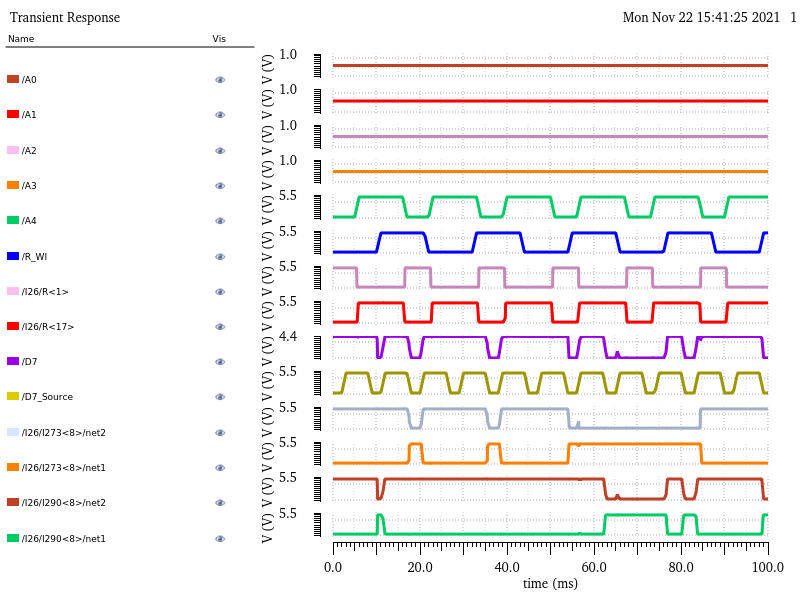
For
this simulation I'm testing out pulsing address bit. In this case all
address are set to 0 except for A4 which is pulusing thus we either
write to location 00000(R<1>) or 10000(R<17>). Outside of
that all other parameters remain the same as our other simulations.
R<1> D7 Sram cells are 1273 and R<17> sram cells are 1290.
As we can see we successfully manage to write to both address since you
can see that the d side shifts from 5v to 0v after D7_Source(0V)
successfully writes it to 0v.
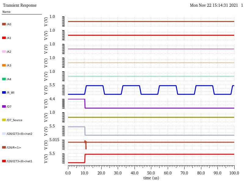
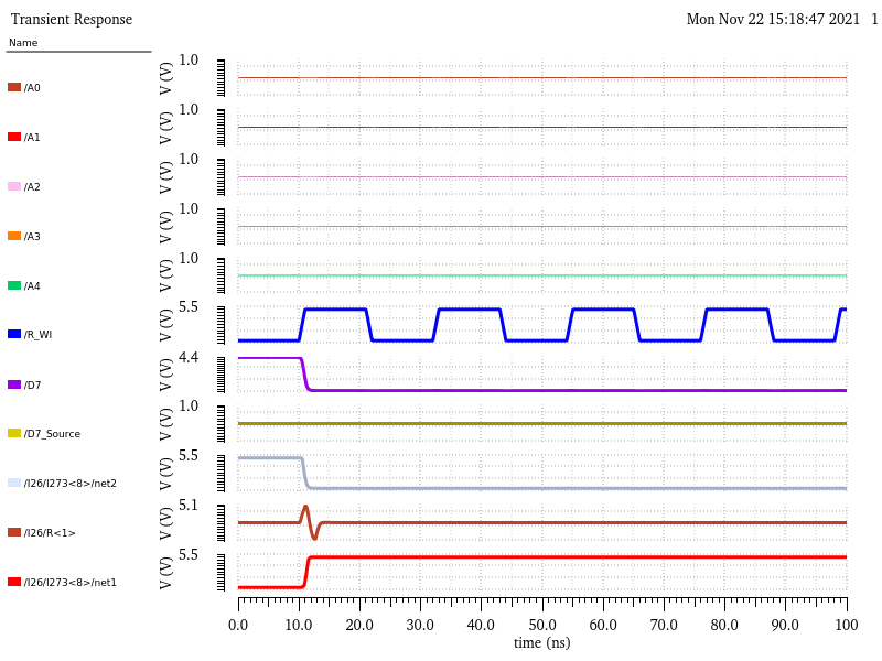
Same as previous simulation however this time I increased the speed(microseconds) to look for any errors or differences.
Same
as previous simulation but now operating at a faster speed(nanoseconds)
as with simulation 1 it becomes appearant that this design will be
susceptible to errors at faster speeds since we're able to see the
delay for a value to take place in the sram cell. The main problem that
arrises is that there is a chance that data doesn't fully settle due to
delay and stays at an invalid logic level.
Simulation 3
For
this simulation I'm now testing the pulsing address bit(A4) alongside a
pulusing data source. As with the previous case we're writing/reading
from either address 00000(R<1>) or 10000(R<17>). We're
either inputting 0 or 5V to D7. 1273 represents R<1> and 1290
represents R<17>. net2 represents the D side of the sram cell and
net1 represents the D_I side of the sram cell. From the simulation
above my design is able to handle changing data inputs.
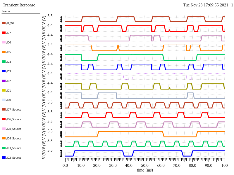
For
this simulation I set out to test multiple pulsing data sources. In
this case D7 & D6 are pulsing. I decided to remove the the address
bits to allow for more room in my screenshot. Like previous simulations
we're either writing to 00000(R<1>) or 10000(R<17>).
1273 represents R<1> and 1290 represents R<17>.
<7> represents 7th instance of my sram cell(D6) and <8>
represents 8th instance of my sram cell(D7). As shown above I was able to successfully write to both address with multiple pulsing data sources.

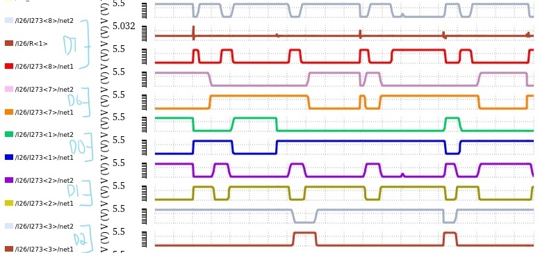
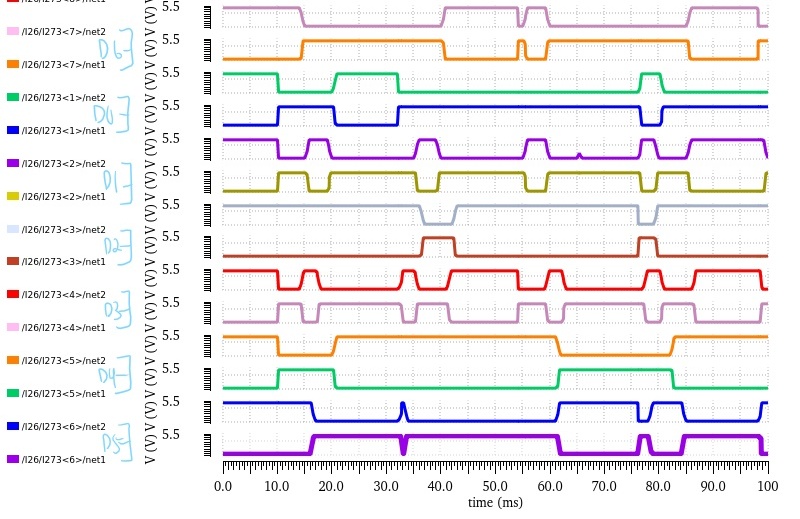
For
this simulation I'm testing pulsing signals for all data inputs all
running at different times. I'm only testing writing to a single
location so I removed the address bits from the simulation output since
they're not changing. Once again net2 is the D side of the sram cell
and net1 is the D_I side of the sram cell. From my simulations I can
see that all my input bits function and no errors occur when writing
with pulsing signals at all data inputs.
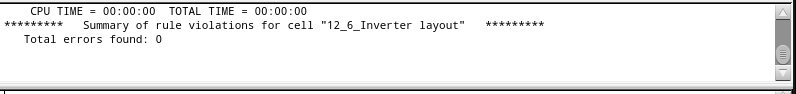
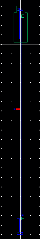
Part 3: Layouts
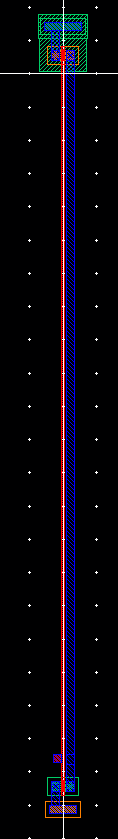
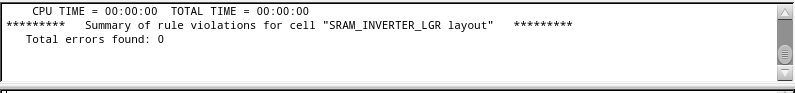
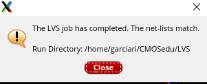
| 1 | SRAM Inverter
Layout
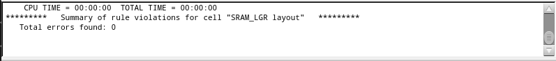
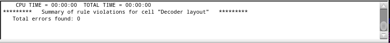
DRC
Extracted
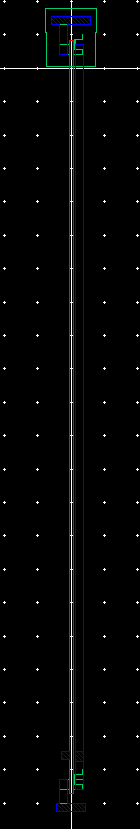
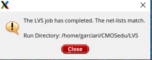
LVS
Pictured
above is my layout for the SRAM Inverter. I designed it so that the
height is same as other cells to make it easier for interconnecting the
VDDs and GNDs with other components. |
| 2 | 12u/6u Inverter
Layout
DRC
Extracted
LVS

There
isn't much to say right now since laying out these individual parts
isn't really a complex task. The layouts changed overtime as I got to
the more complex modules in which I needed to move around pieces and
mess around with sizing to get the layouts to pass drc. |
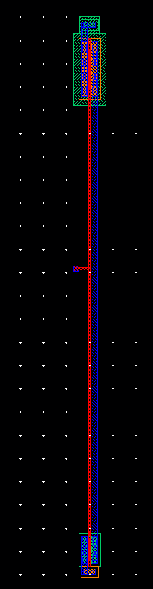
| 3 | SRAM Cell
Layout
DRC
Extracted
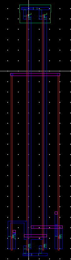
LVS
This
cell was the layout that I ended switching around alot to be able to
fit into DRC rules. It was mostly due to the fact that compared to the
NAND gate where it only took in 1 input(Address or complement Address)
this cell took in both D and complement D. So I had to mess around with
the placement of rowline, D, and DI pins to be able to keep the design
concise uniform and within DRC rules. |
| 4 | 5 Input NAND Gate
Layout
DRC
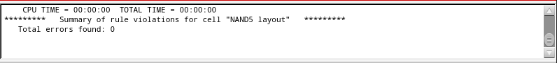
Extracted
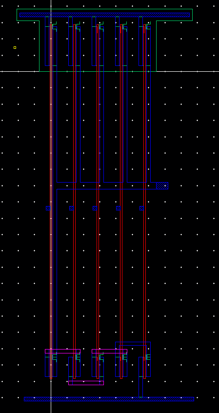
LVS

This
design wasn't as bad compared to the SRAM cell since I could use any
point of the long poly and metal 1 lines to attach my input to so there
wasn't any problem with fitting into DRC rules. |
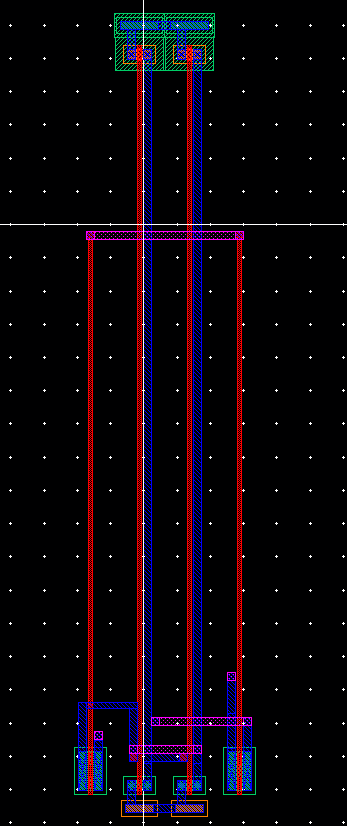
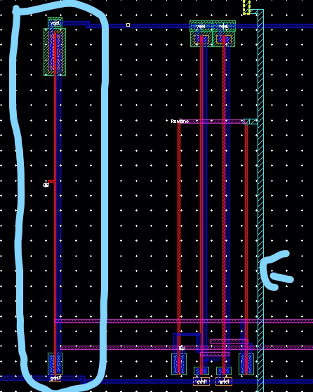
| 5 | Row Decoder
Layout Part 1
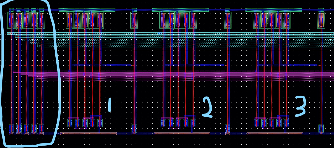
Layout Part 2
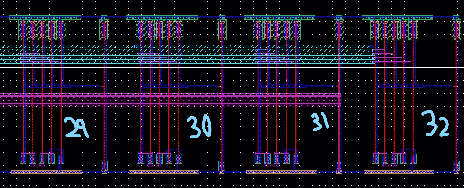
DRC
Extracted
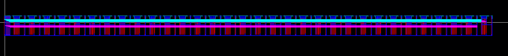
LVS

This
where the layouts begin to get really complex. For our row decoder we
use 2 of our previously created modules the first being our 12u/6u
inverter and the second being the NAND gate. The circled part in Layout
Part 1 Image represents the inverters that take in our address inputs
and create a complement of the inputs. The complements are on metal 2
while the original address bit is on metal 3. I next intiated 32 5
input nand gates to represent all 32 possible address. I connected all
the possible address to a nand gate. The nand output is connected into
an inverter to produce the actual rowline input for the sram cell. The
second layout image represents the last 4 NAND gates. |
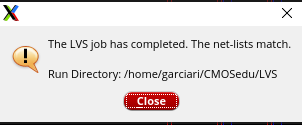
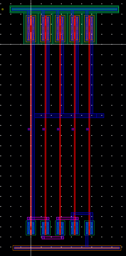
| 6 | Register File
Layout Part 1
Layout Part 2
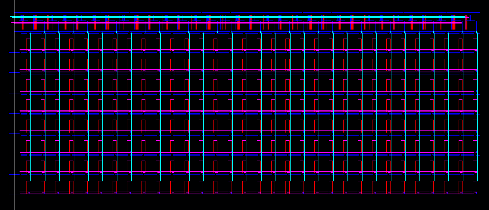
DRC
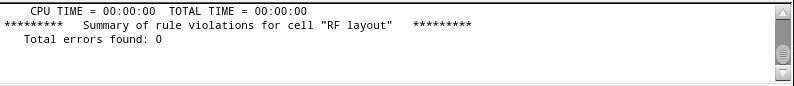
Extracted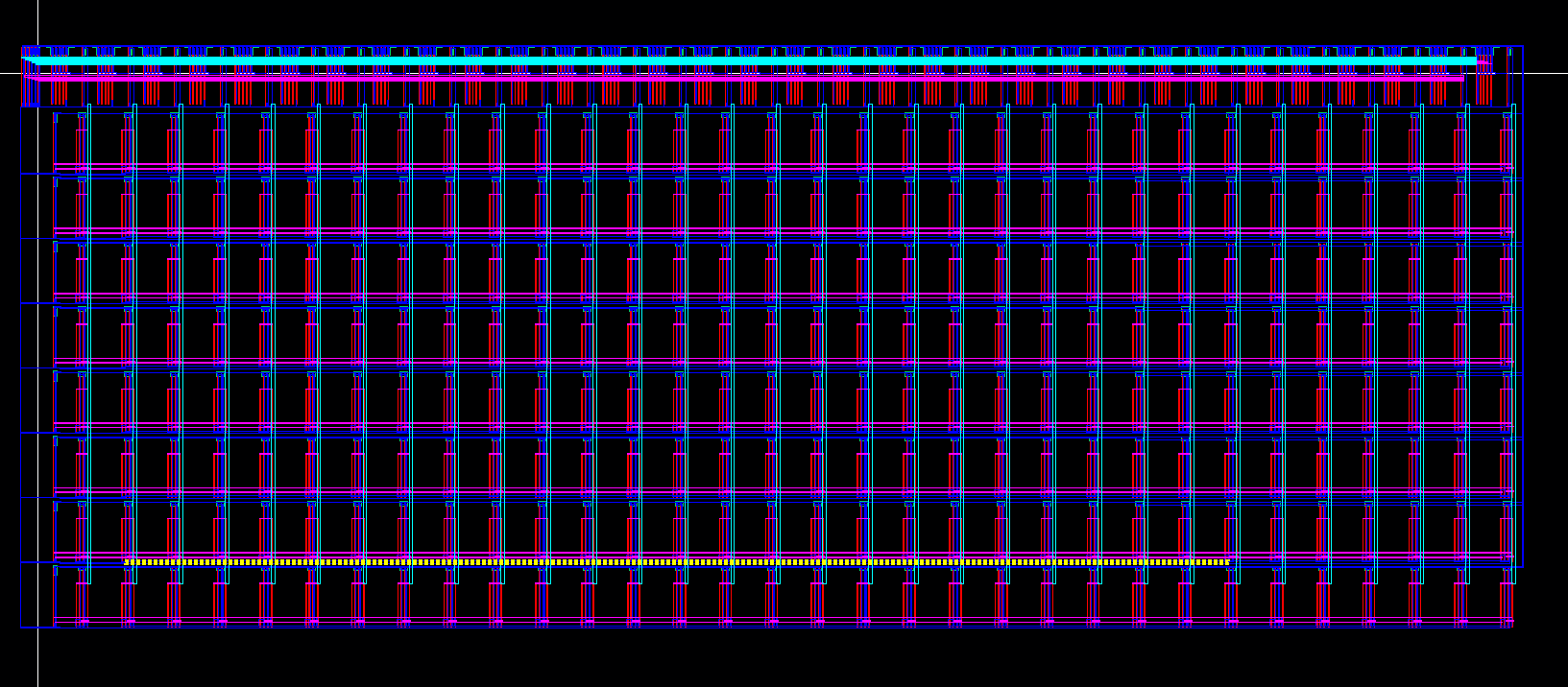
LVS
For
my RF layout I first instantiated my row decoder so that I could get
all the R<n> outputs that will be used to turn on the SRAM bit
cells. This is the top layer of my layout. Beneath the top layer is my
32 column by 7 row sram cells. Each row represents a dataline with the
highest vertically representing D0 and the bottom row representing D7.
Thus each singe word is a column. The first layout picture shows the
data input being inverted and connected to the first address sram cell.
Also shown in the picture the metal 3 layer that connects the row
decoder rowline output to the sram cell. The only major thing that I
would change about my layout would be flipping my sram connections so
that the it would actually be rows instead of columns for each word
like it is now other than that I feel that my layout was good. |
Conclusion:
I
throughly enjoyed this lab; it felt like a nice way to reinenforce
what've learned in my lab. The lab forced me to use all the concepts
that I learned during my time at the lab. I also liked that the lab was
open as to allow me to design it myself. The recommendations by
Dr.Baker were really helpful not just because He told me the best way
to go about designing the RF but also because it allowed me to reflect
on my 421 knowledge to understand why the recommendation is the best
design to go with. The only thing I would go back to change to improve
my design is to put more emphasis on timing as seen in my simulations
at higher speeds i.e. nanoseconds delays start to become promient which
will only lead to errors. However, since we were told not to worry
about speed I'm satisfied with my final design for this class.
Download Link for Design Files:
LAB_FinalProject_LGR.zip
Return to EE421L Labs