| 1a | The
first step of this lab is to layout 2 CMOS inverters. For my first CMOS
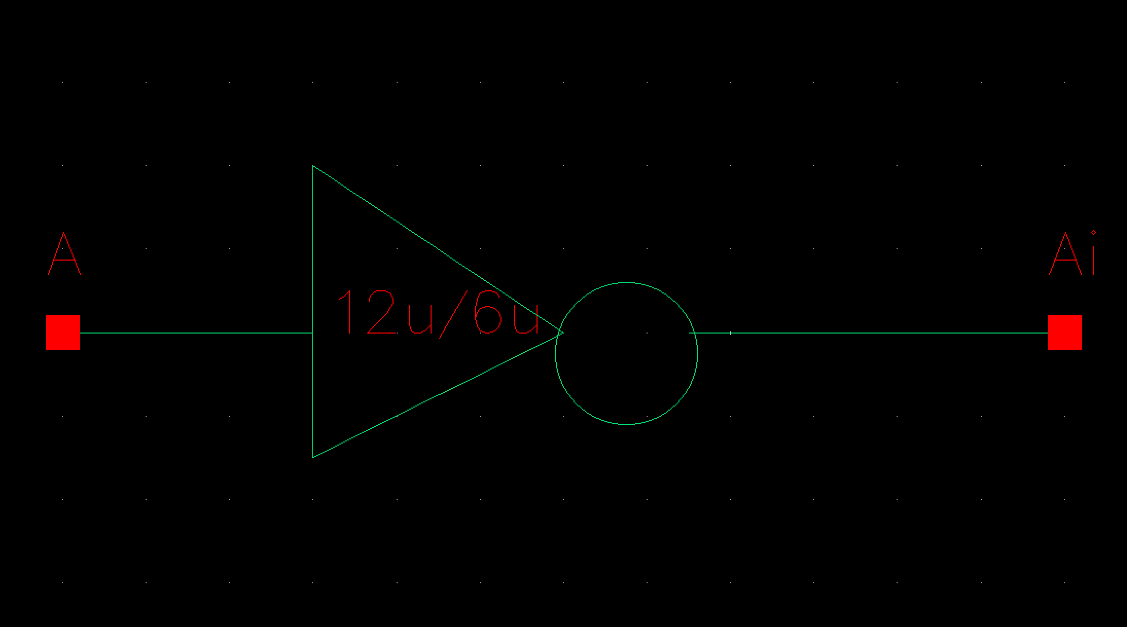
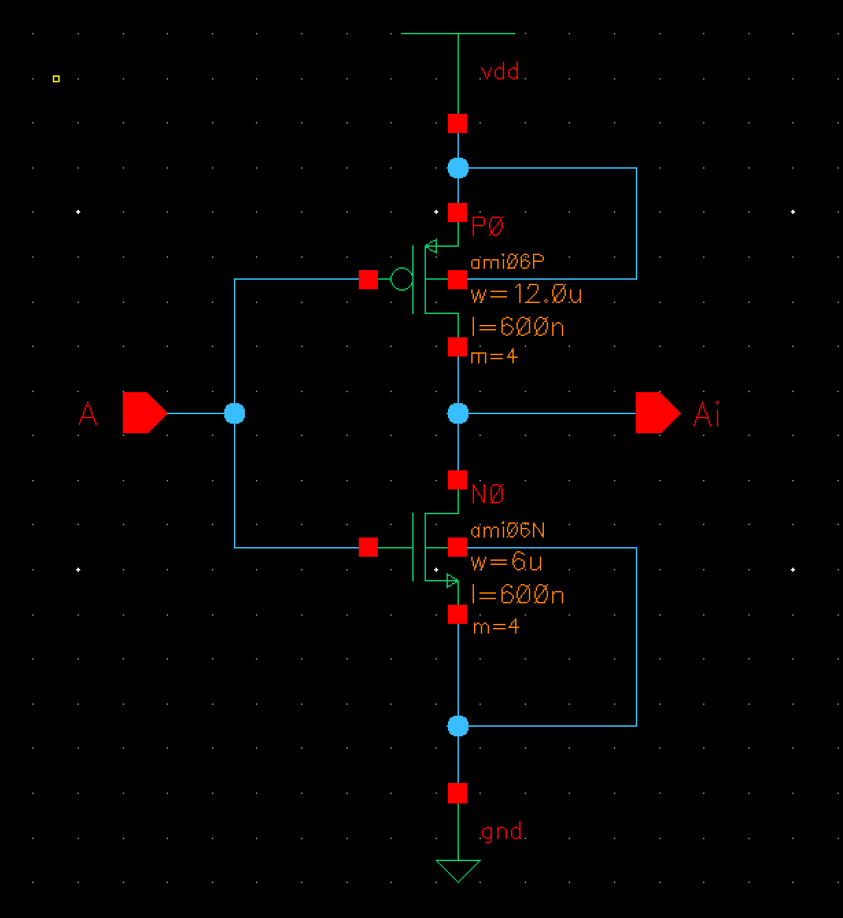
it is the same as the tutorial 3. A 12u/6u CMOS with the lengths of .6u.
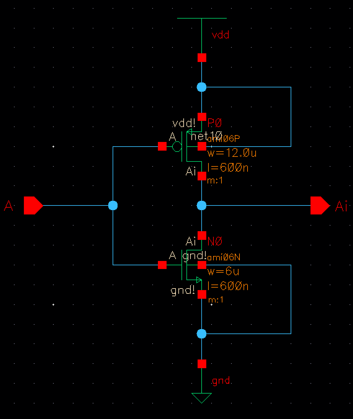
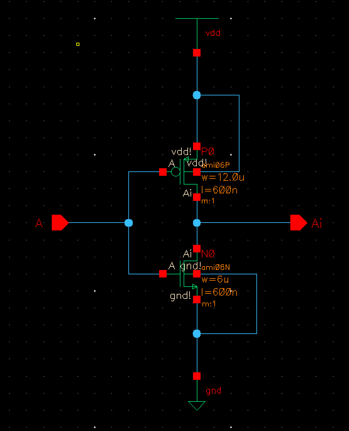
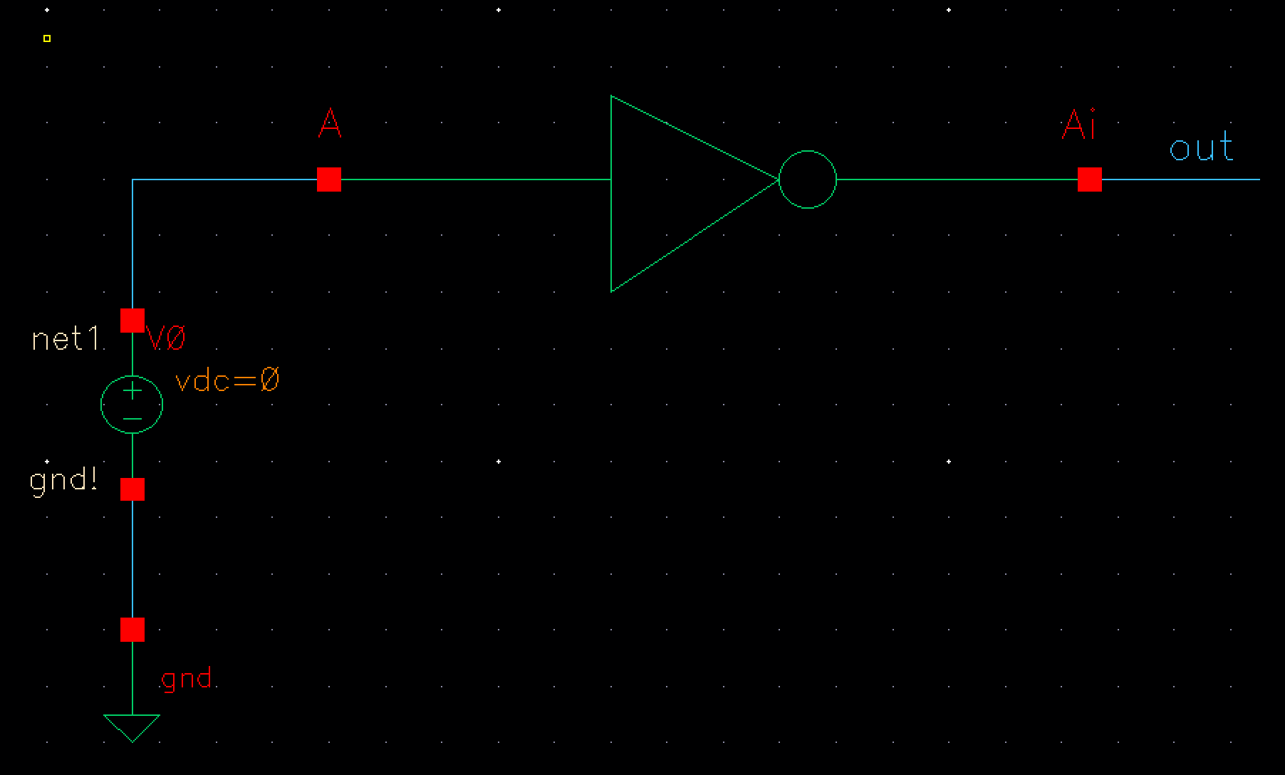
As in tutorial 3 we start by creating a schematic of our CMOS inverter consisting of a PMOS connected with an NMOS.
After
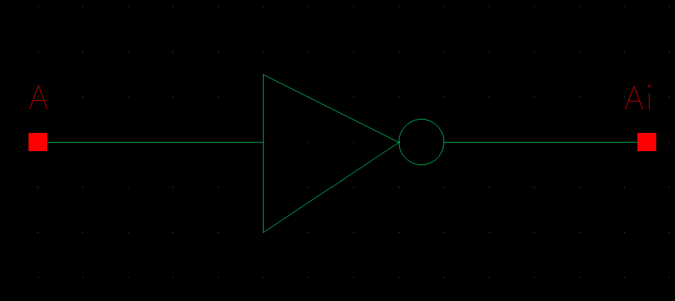
creating the schematic I next created a symbol. This followed the same
steps as the tutorial. I erased the premade symbol and create a more
appropriate symbol. This time however I added the text that tells me
which CMOS inverter I'm using to avoid confusion in the simulation
later on.
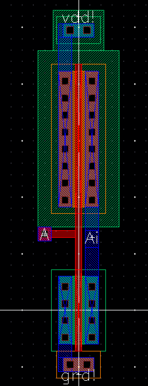
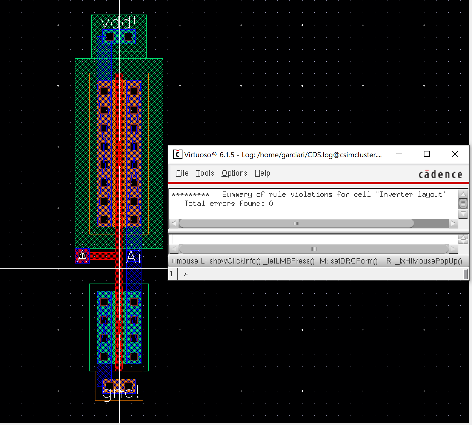
After creating my symobl I next created my layout which is the same as the tutorial since they're both 12u/6u CMOS inverters.

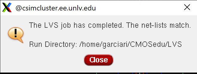
I drc'd my layout then proceeded to the next step which is extracting my layout.
After extrating my layout I next LVS'd my extracted layout to make sure I had successfully layed out my 12u/6u CMOS Inverter.
 |
| 1b | For
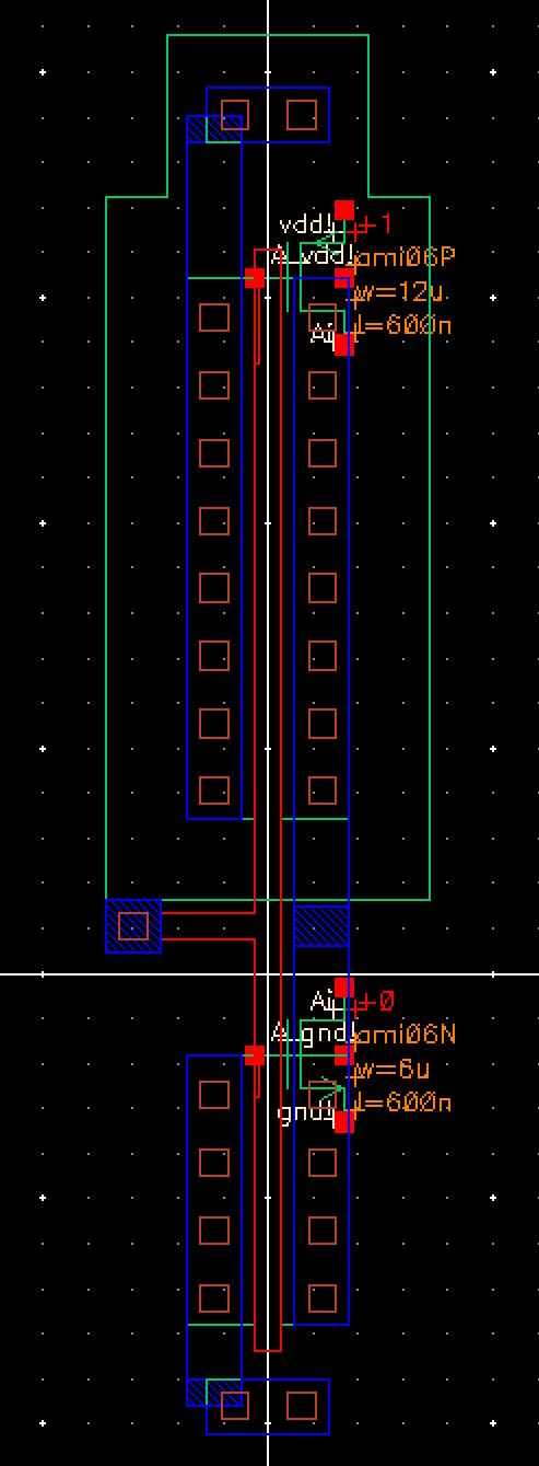
the step 1b I next proceeded to layout a 48u/24u CMOS inverter. This
step is the similar to the 1a step and tutorial 3 except for the
inclusion of fingers. For this CMOS we're laying out using 4 fingers
which means we're laying out at a single 48u/24u CMOS that consists of 4 12u PMOSs and 4 6u NMOSs.
Again
I first start my layout by creating a schematic. This is the same as in
tutorial and step 1a however this time I must include 4 fingers in my
MOSs. I did this by inputting 4 into the mulitpiler fiield which tells
cadance that my MOSs will have 4 fingers or 4 MOSs next to each other.
I
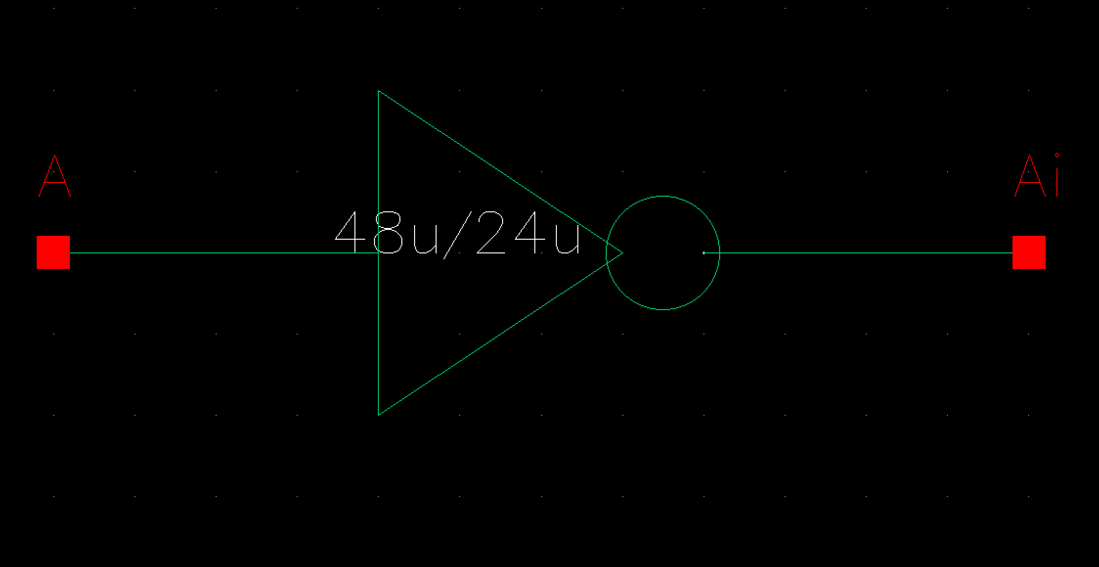
next created a symbol of my schematic this step is exactly the same as
in step 1a and tutorial 3. I added text specifying that this CMOS
inverter is a 48u/24u to avoid confusion later on.
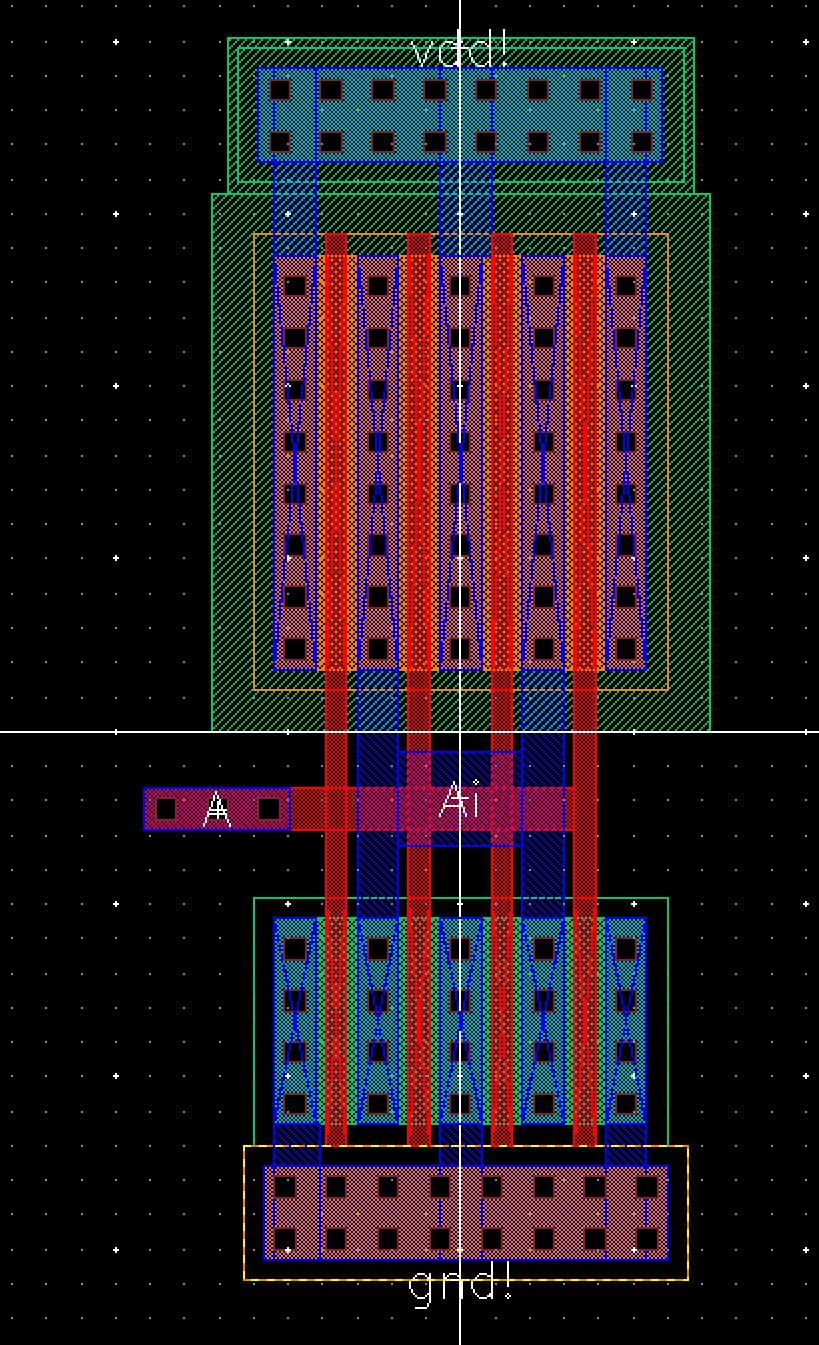
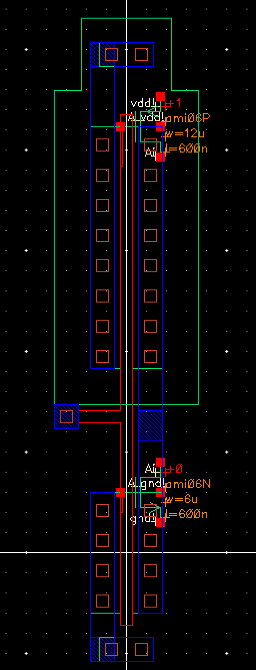
The
next step is to layout my schematic. My layout lets us see exactly what
4 fingers means. 4 fingers refers to the addition of 4 poly lines going
down our MOSs this results in the creation of more MOSs without
having to increase length. In this case we we're able to create 4 12u
PMOS and 4 6u NMOS. Despite the radical difference in this layout
compared to the layout in step 1a and tutorial 3 we still follow the
same steps. I interconnect our Poly's and connect these polys to our
m1_poly. After this I interconnect our PMOS Source with our NMOS Drain.
I next connected my PMOS drain to VDD and my NMOS source to GND. All
that was left after this was add pins to specify our inputs
,inputoutputs and outputs.

After completing my layout I drc'd my layout. As seen above it successfully drc'd. I next extracted my layout.
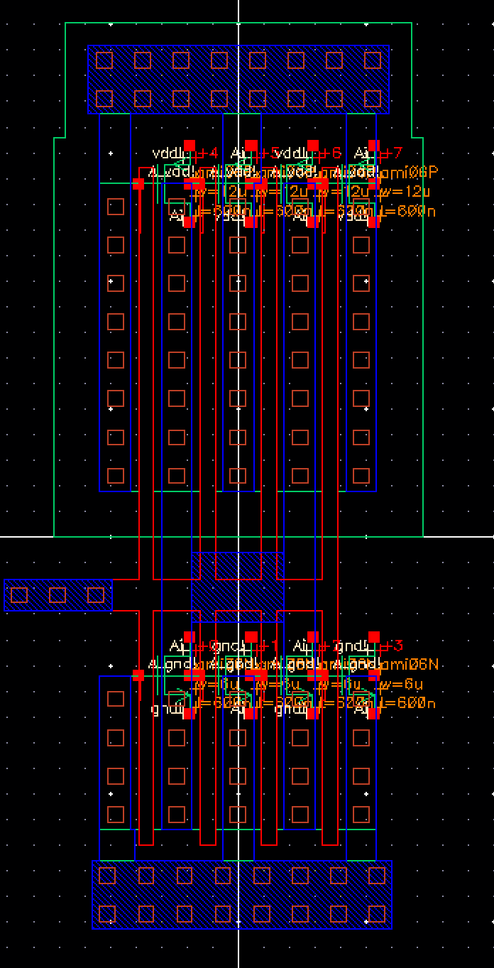
After extracting my layout I next run an LVS to make sure I successfully layed out my 48u/24u CMOS Inverter.

I have successfully layed out my 48u/24u CMOS inverter. |
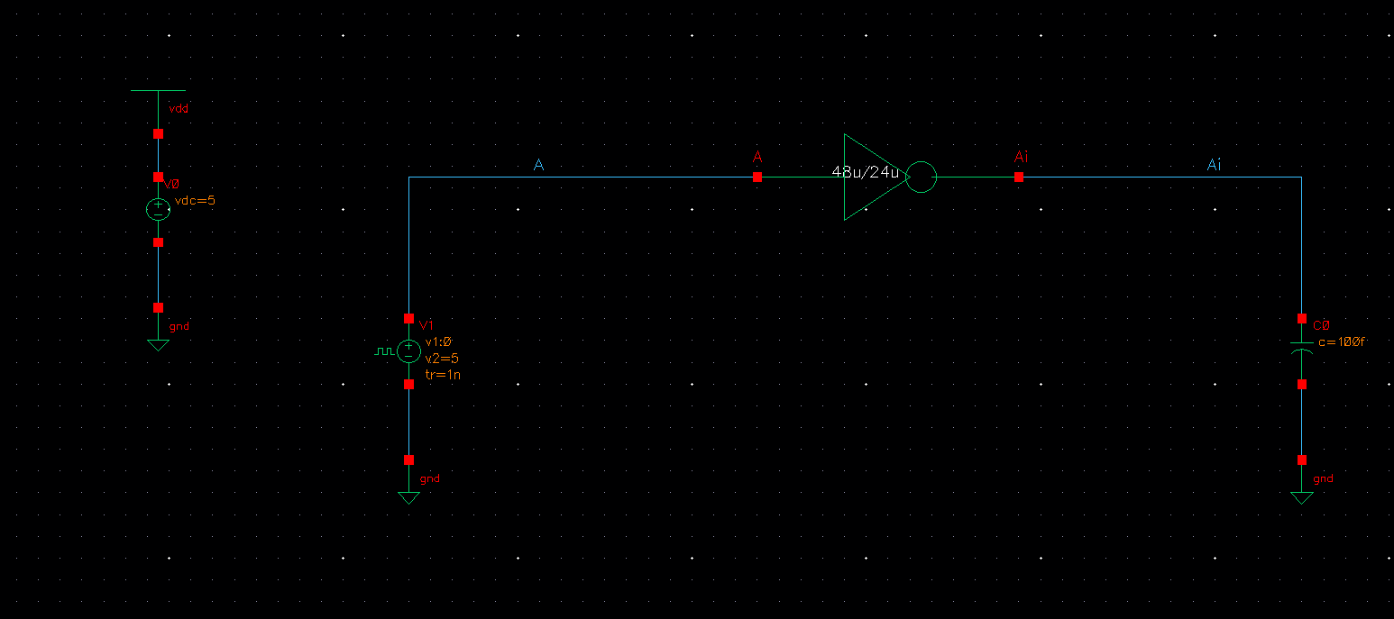
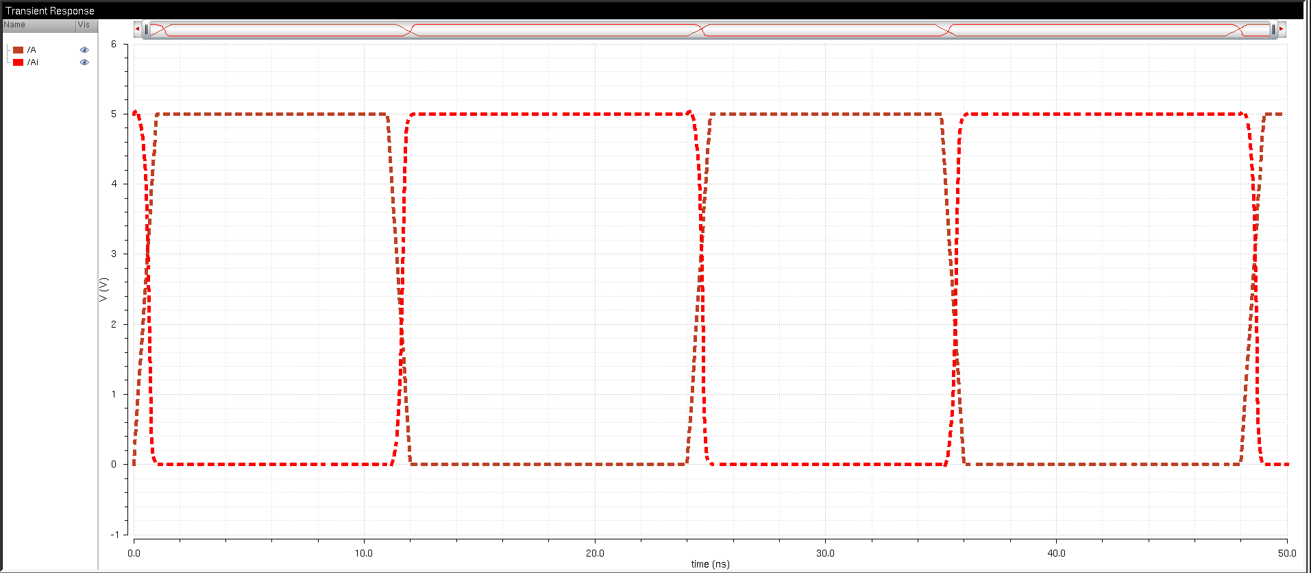
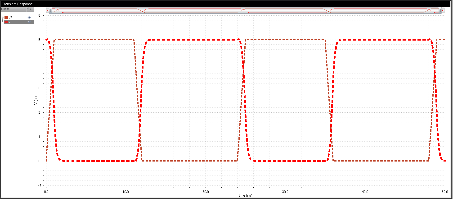
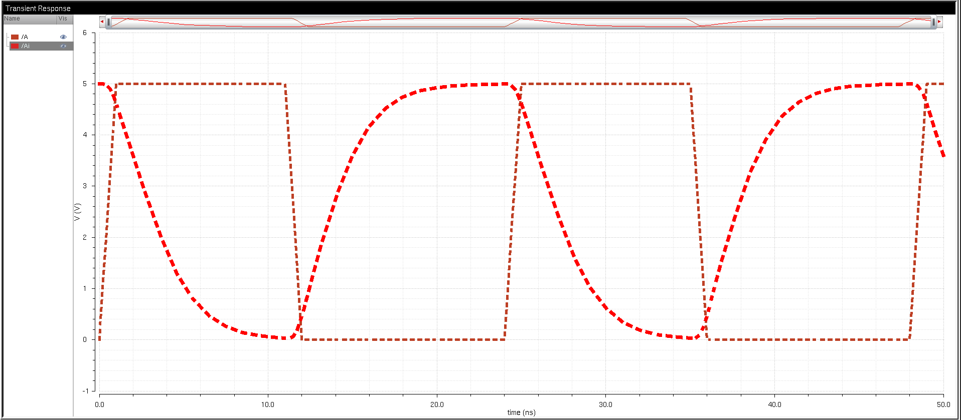
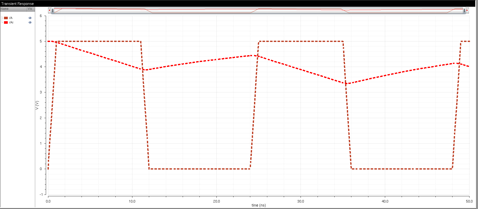
| 2a | I next ran simulations using my 12u/6u CMOS Inverter.
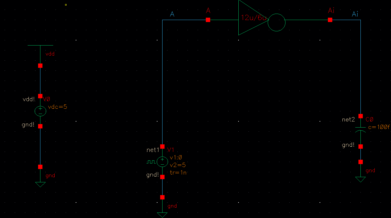
First
I created a schematic which consisted of VDD connected to a 5V DC
voltage source. A pulse voltage signal connected to our 12u/6u CMOS
Inverter, then a capacitor connected to the output of our Inverter.
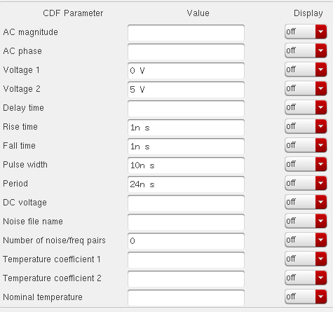
Above is the settings used for our voltage pulse signal.
After
setting up my schematic I ran transisent analysis for different
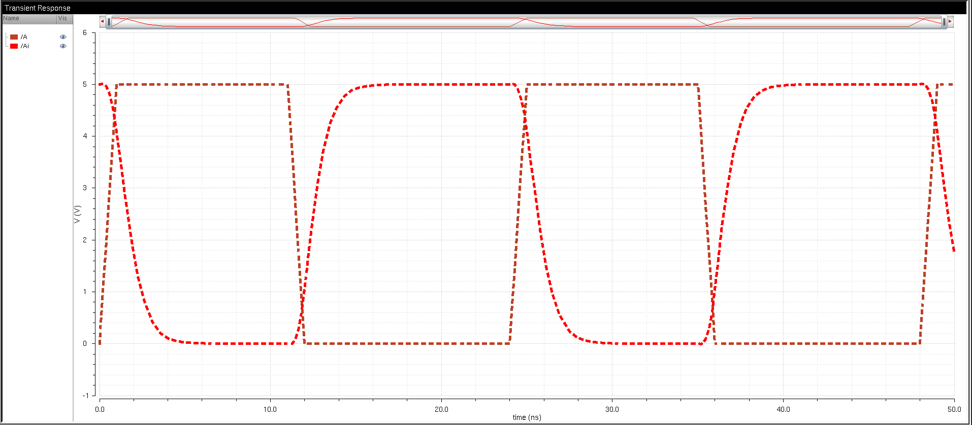
capacitors. Our capacitors consisted of 100fF, 1pF, 10pF and 100pF.
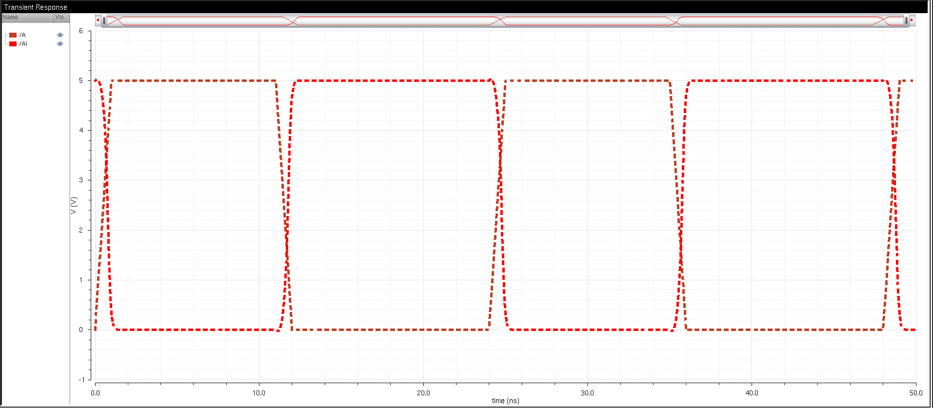
100fF
1pF
10pF
100pF
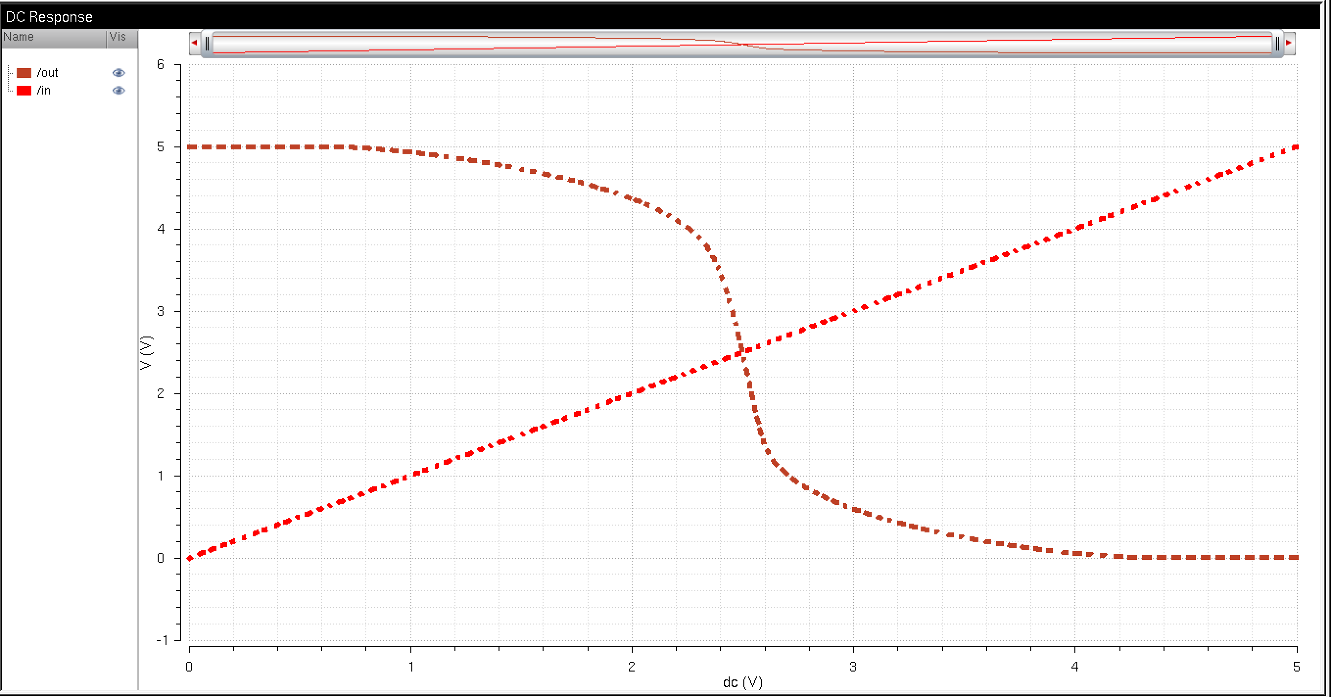
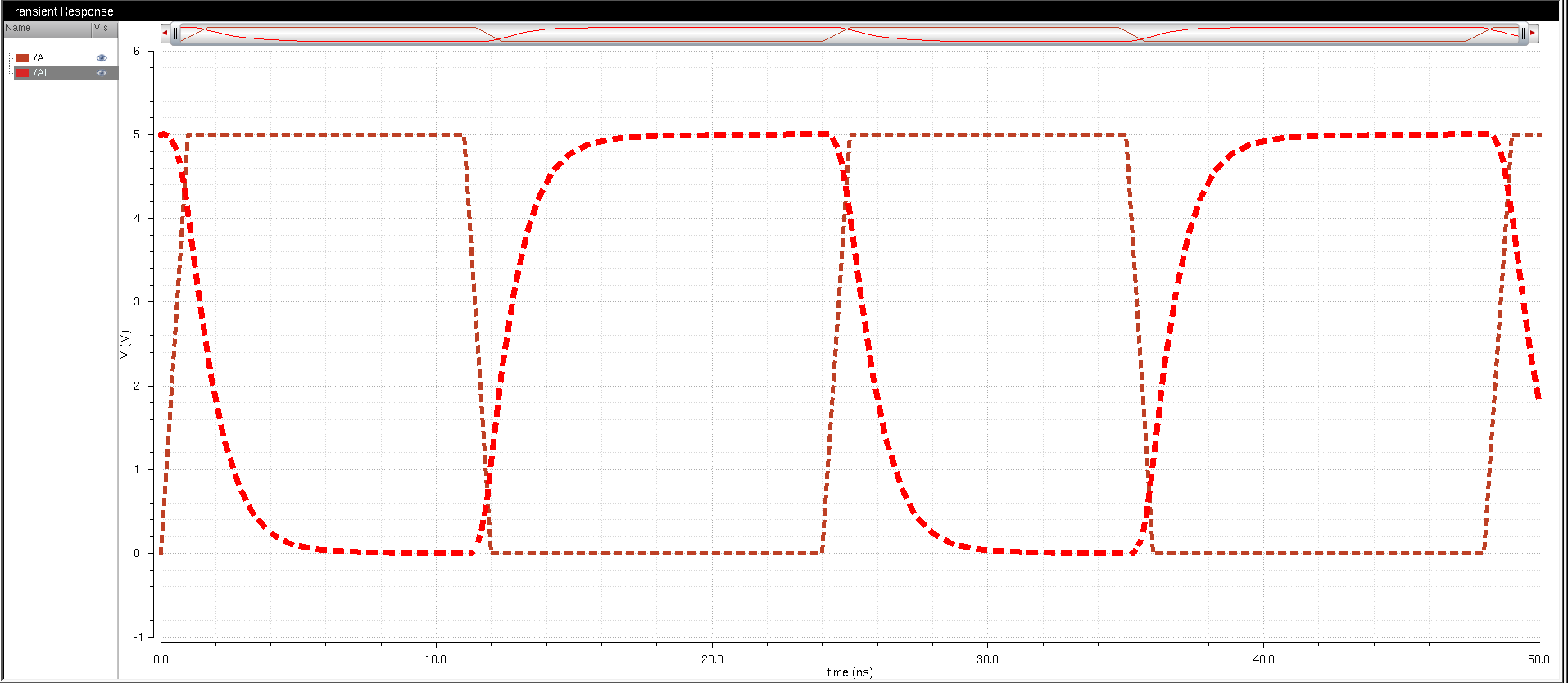
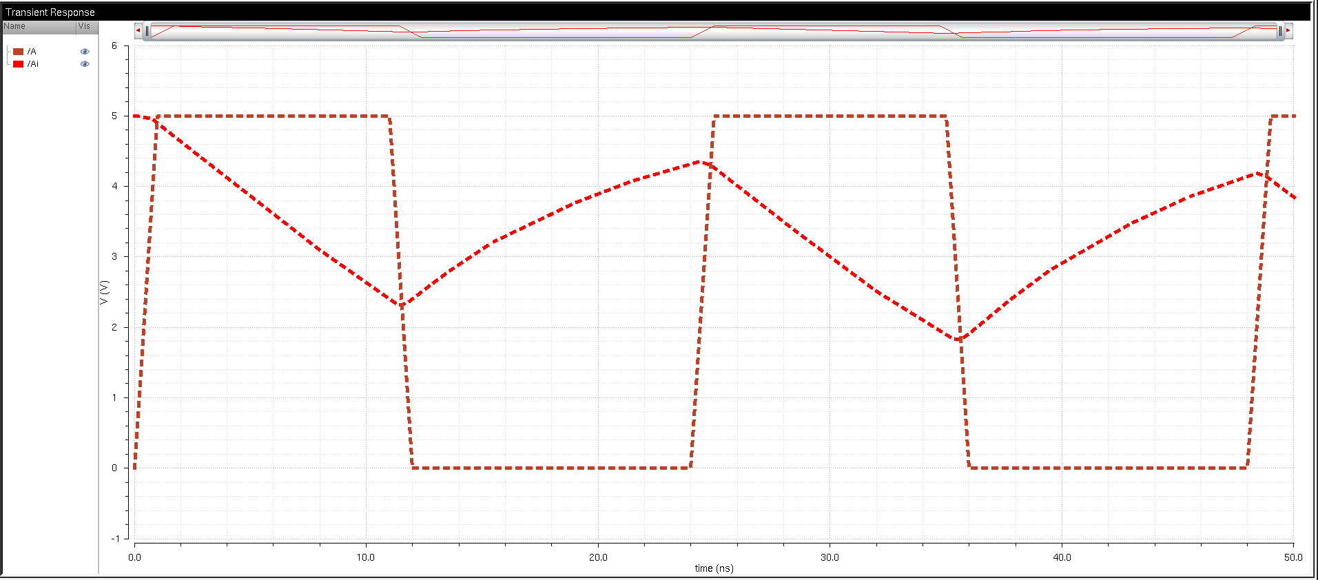
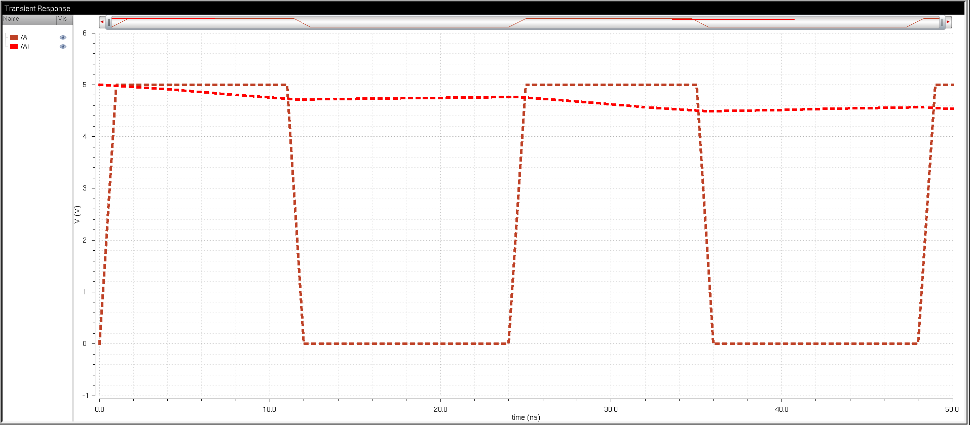
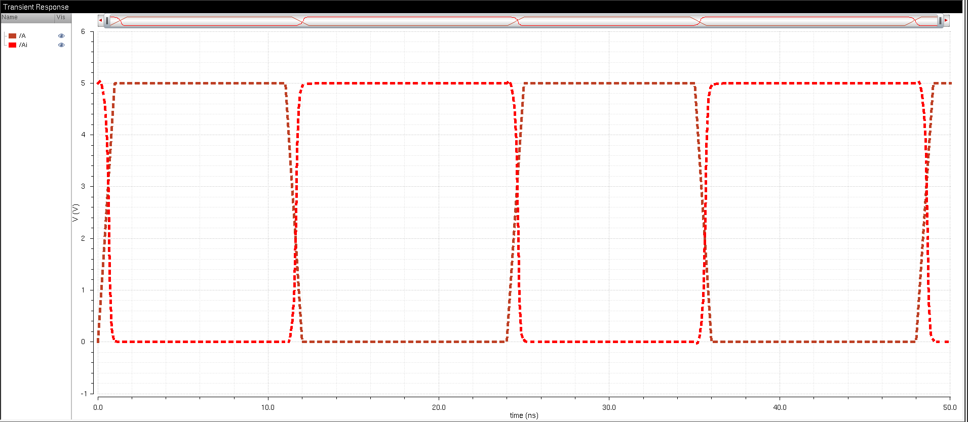
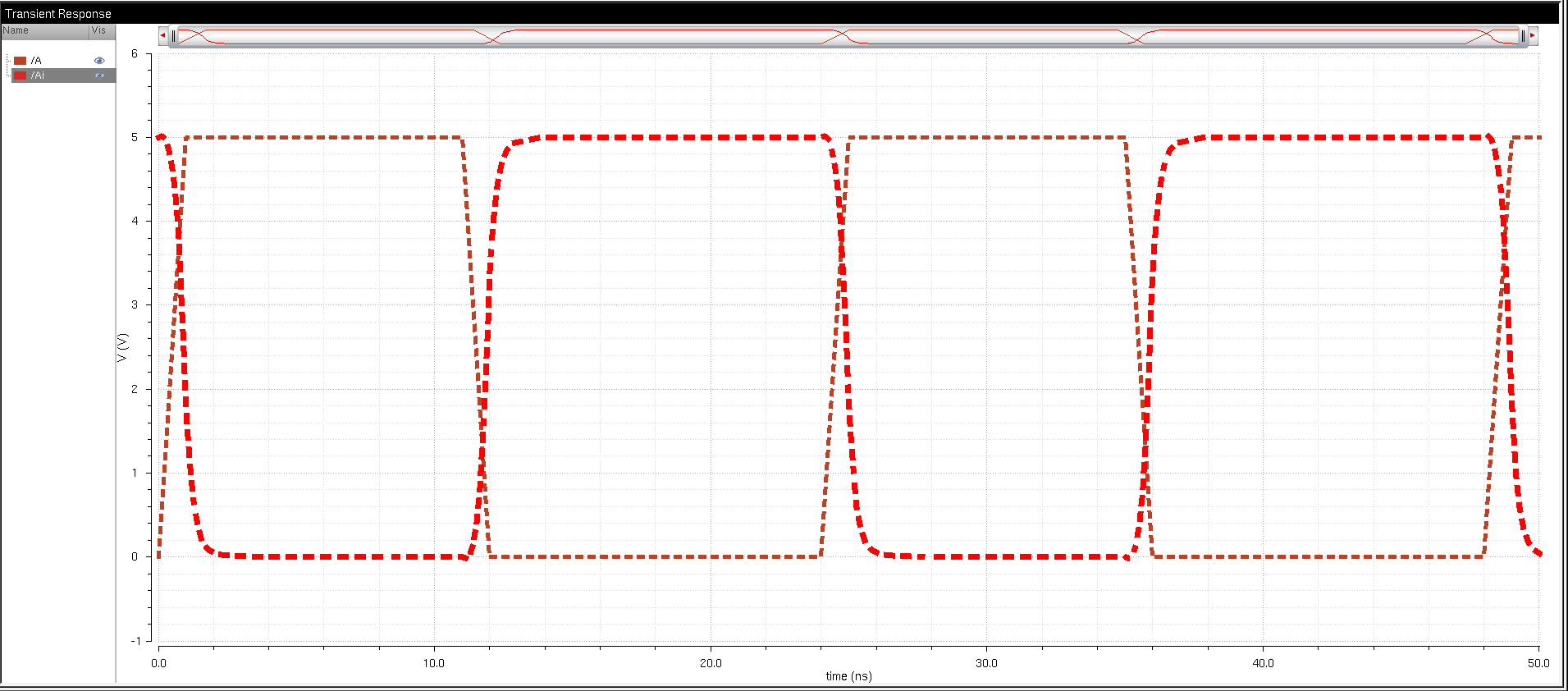
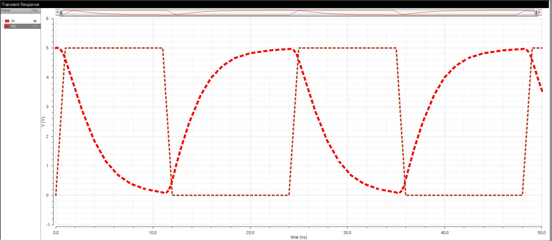
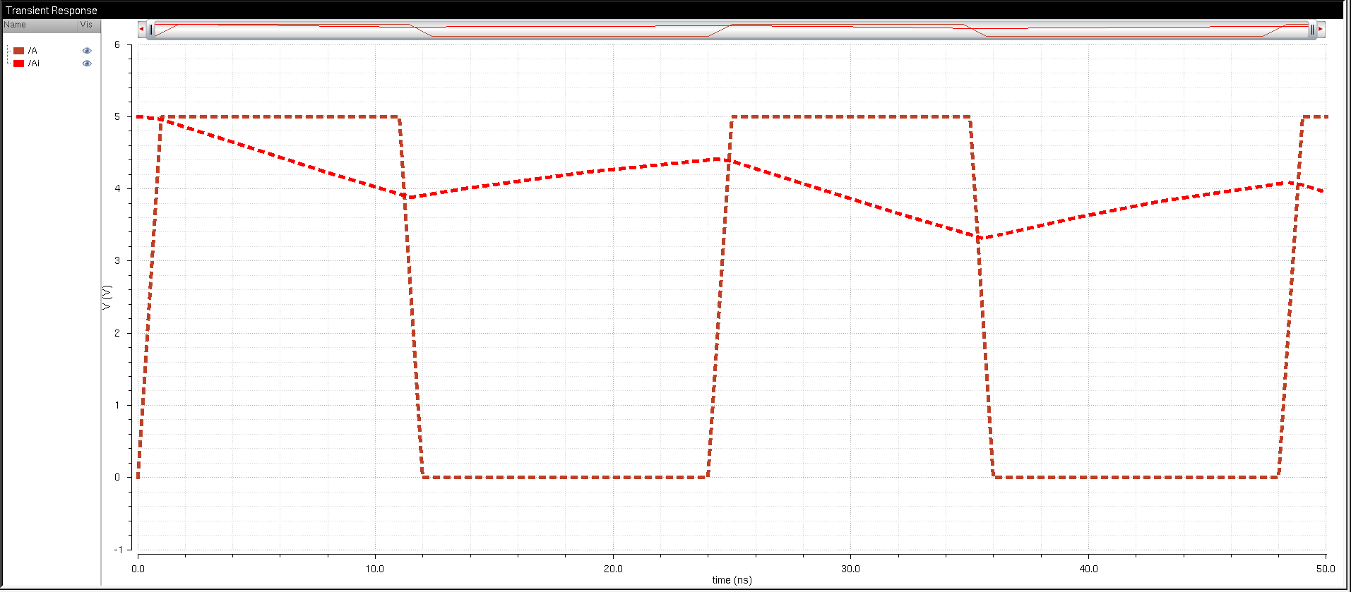
The
first thing I noticed is that my CMOS Inverter is in fact working, when
our input is high our output is low and when input is low our output is
high. This is very evident in the 100fF capacitor transisent response
graph. The second thing I noticed is that as we increased the capacitor
size our graphs began to not be inversely related to our input. This is
due to the fact that our capacitors increased in value thus they were
able to hold more charge before dissapating. This is very evident in
the 100pF capacitor transisent reponse graph in which we see that we
are close to achieving a constant output. |
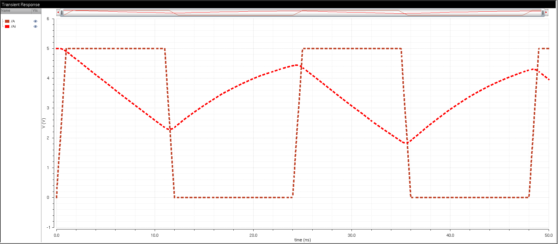
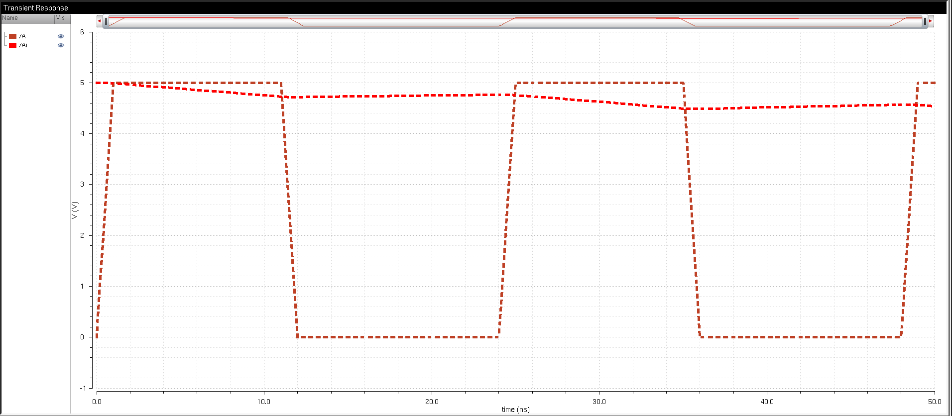
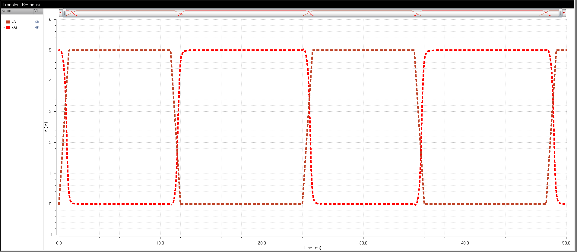
| 2b | For step 2b we follow the exact same steps as steps 2a except this time we are simulating using our 48u/24u CMOS inverter. We start by first creating a schematic.
Our schematic is exactly the same as the 12u/6u CMOS inverter except for the fact we are simulating a 48u/24u CMOS Inverter.

Our
VPulse settings are exactly the same. After completing my schematic I
ran transisent analysis for 100fF, 1pF, 10pF, and 100pF capacitor loads.
100fF
1pF
10pF
100pF
Our
48u/24u CMOS inverter outputs share the common theme that the 12u/6u
had, as I increased the capacitve load my outputs began to get more
straightened out. However, for my 48u/24u CMOS inverter this occured
slower compared to 12u/6u. This can be seen by comparing th 100pF load,
our 12u/6u CMOS inverter output is more straight/constant than our
48u/24u CMOS inverter output. |
| 3a | For
the final step 3a, I simulated the same schematic as in step 2a with
the same loads 100fF, 1pF, 10pF and 100pF. However this time I used the
ultra simSPICE simulator instead of Spectre.
100fF
1pF
10pF
100pF
In
this case, when comparing my ultrasim transisent graphs to my spectre
graphs I really couldn't see any difference between the two. In the
future I will continue to use spectre since the time to create the
netlists and simualtions hasn't to been too bad and because I'd have
accurate results. However, this could possibly change as we simulate
more complex schematics and the speed difference between ultrasim and
spectre becomes noticeable. |
| 3b | As in step 3a, we repeat the simulations that I did in step 2b however this time simulating using ultra sim instead of spectre.
100fF
1pF
10pF
100pF
As
stated in step 3a, I didn't see any noticeable difference when using
Ultra Sim compared to Spectre but as I gain more experience with
cadance I could possibly develop a use case in which Ultra sim is more
appropriate than spectre. For now spectre should suffice. |