Lab 4 Digital Integrated Circuit Design - ECE 421L 

Authored by Luis Garcia Rivas,

garciari@unlv.nevada.edu

September 22, 2021

Prelab

For the prelab I was tasked with completing tutorial 2. Tutorial 2 walks through the process of designing and laying out both P & N mos transistors. In addition to tutorial 2, I was tasked with backing up my previous work which I did by zipping up my lab folder and copying it to an external flash drive.

1Schematic
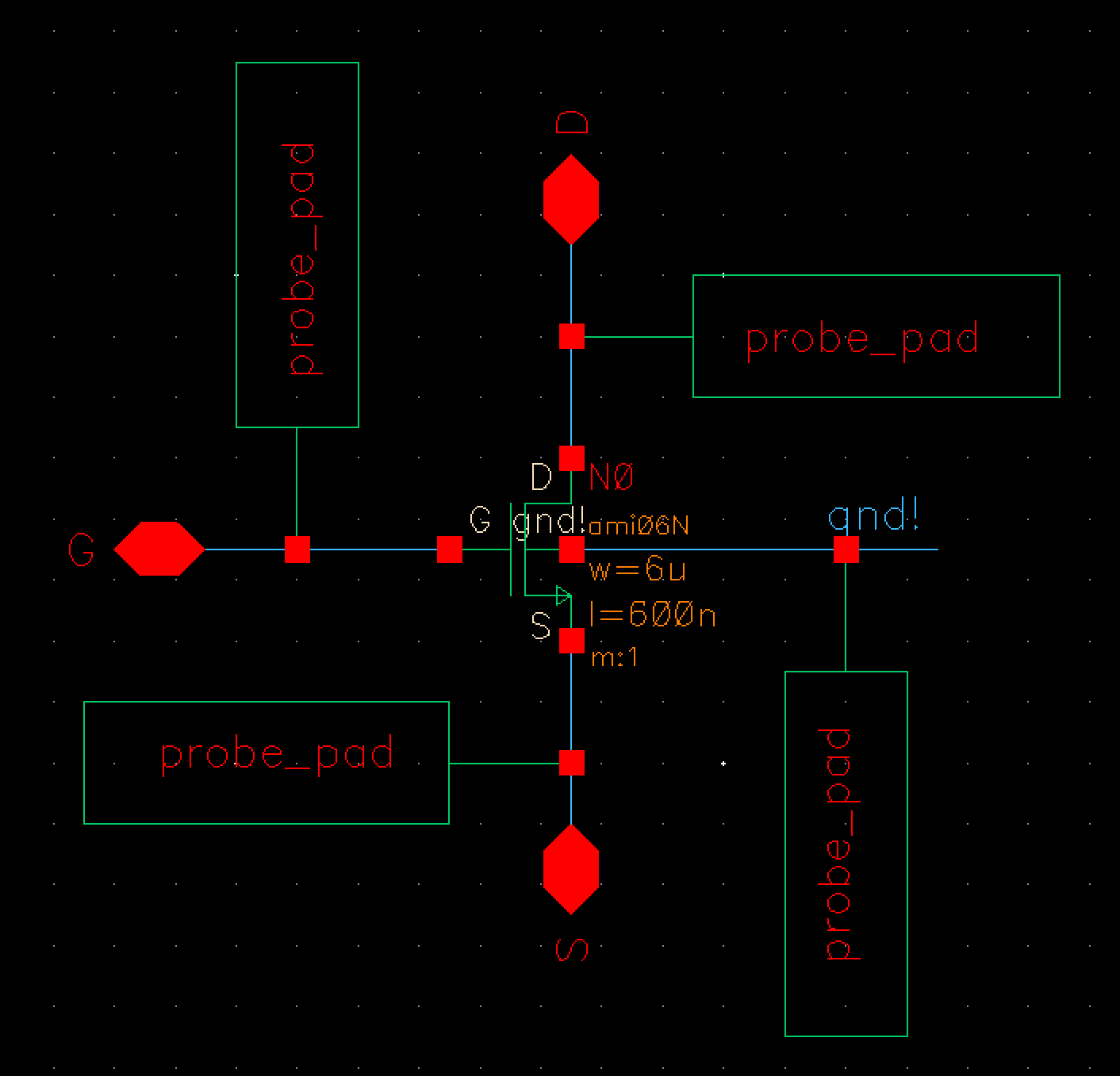
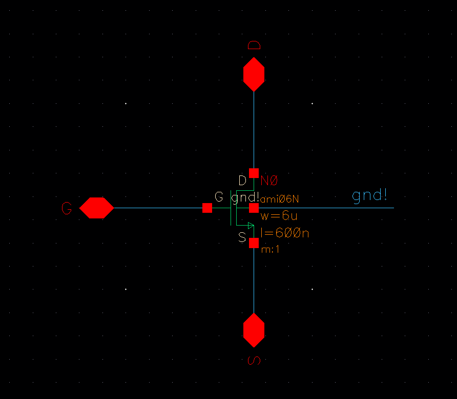
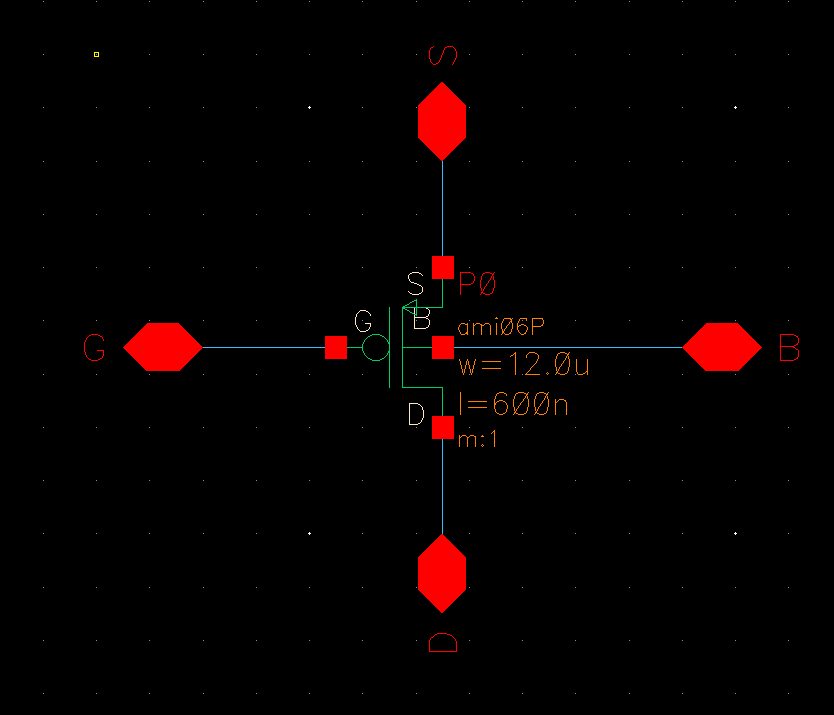
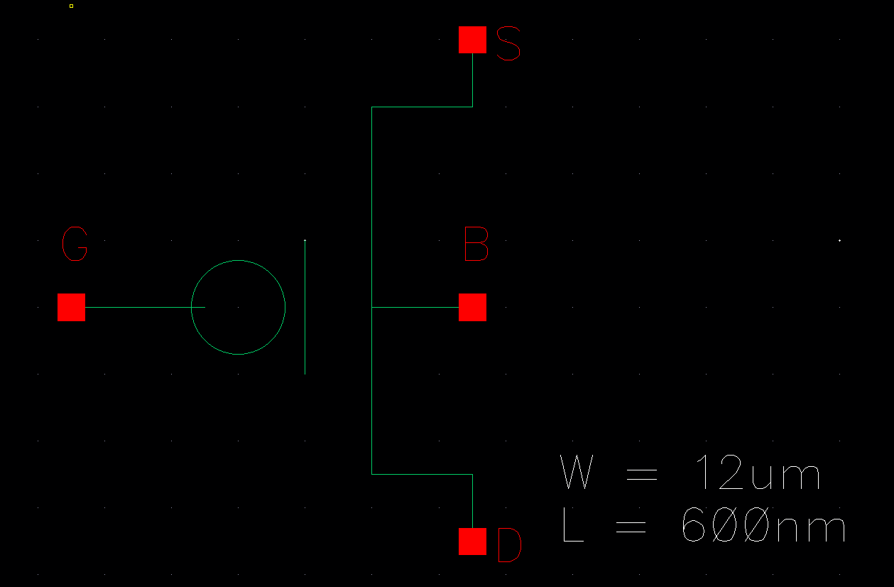
The first step in the tutorial is to create a schematic for an nmos transistor. After creating the schematic I added pins to all the outputs so that we could create a symbol. Initially the tutorial asked me to use an nmos that doesn't include the body connection however this would later cause issues. To avoid reduncy I'll only be including pictures from the revised version of my NMOS that includes the body connection.
2Symbol Schematic
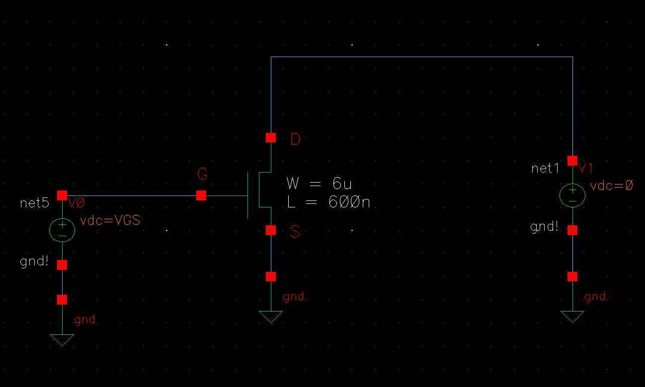
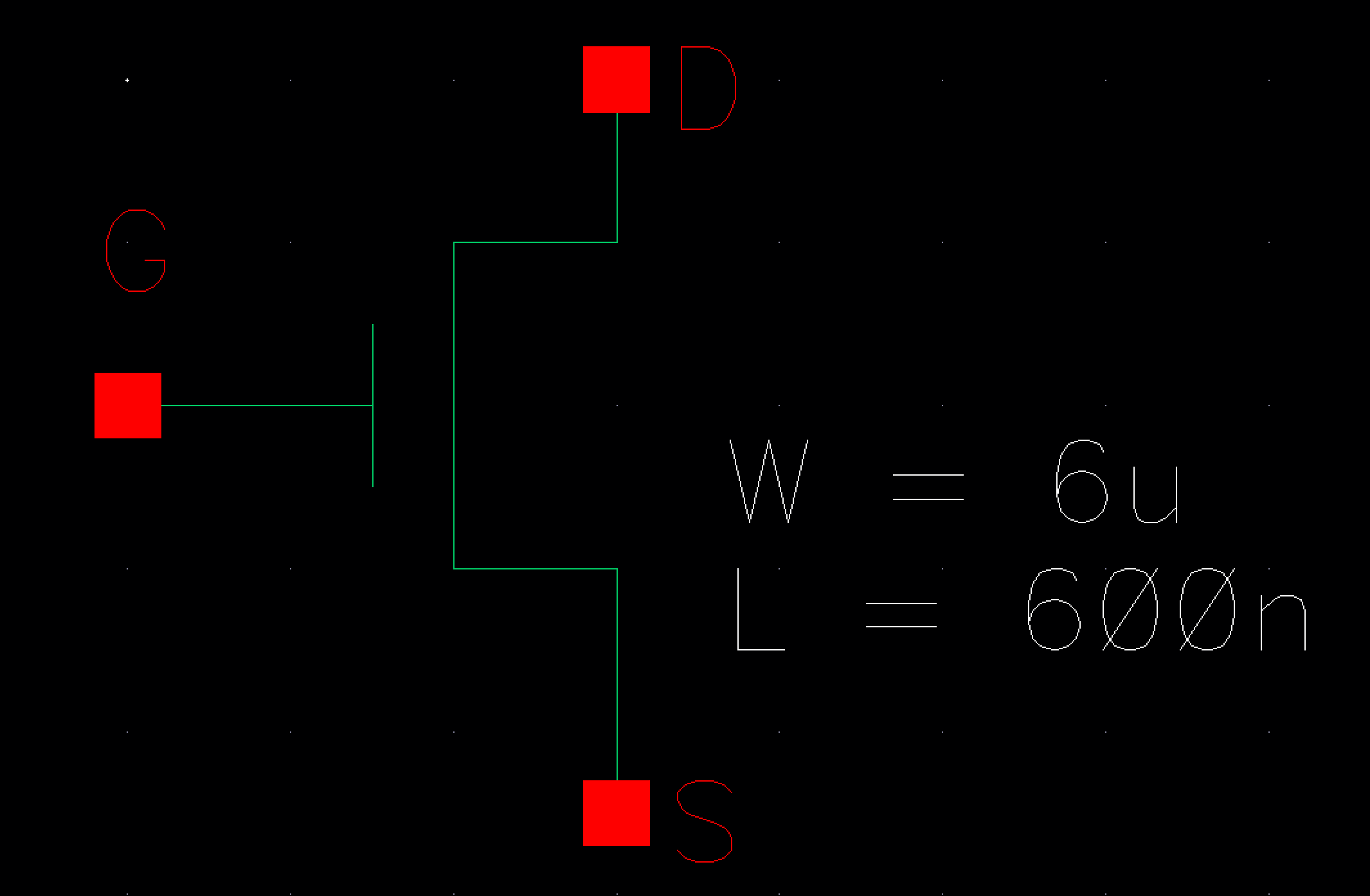
After creating the symbol I next created a schematic using my symbol in order to test and verify that my symbol worked. Above screenshot is my schematic using my nmos symbol.
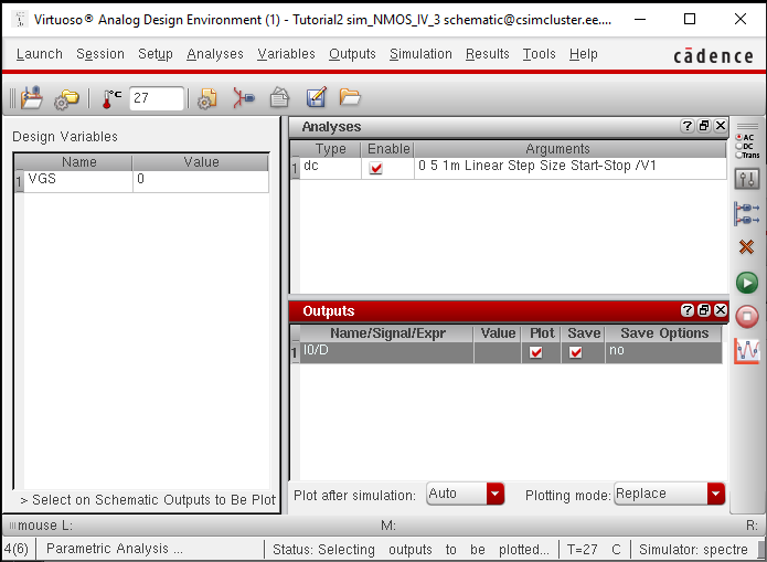
ADEL Settings
ADE L Settings
Parametric Settings
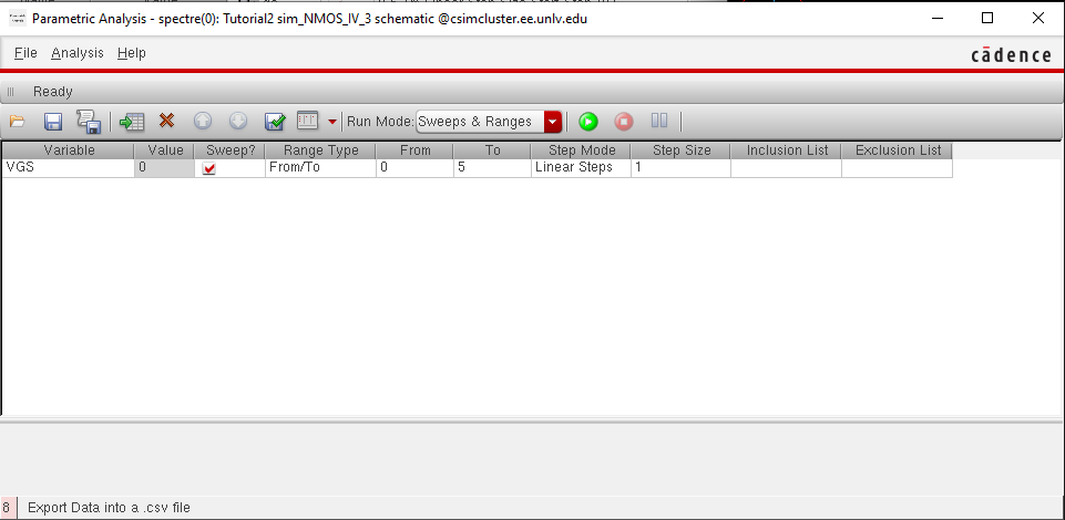
Parametric Analysis settings
Transisent output
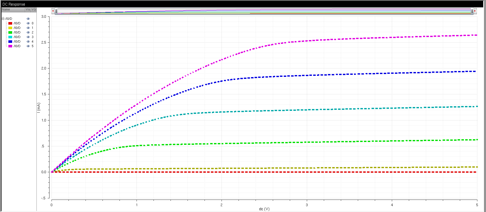
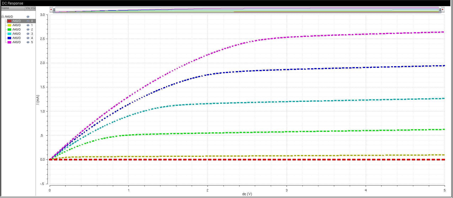
My NMOS symbol transisent analysis confirming that our symbol was working as intended.
3Layout
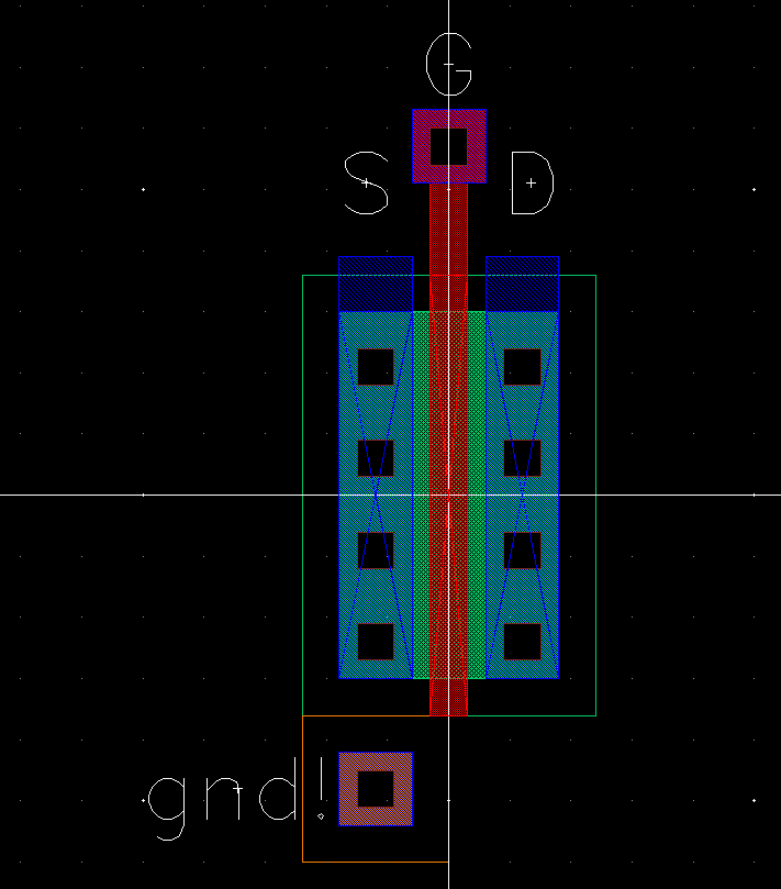
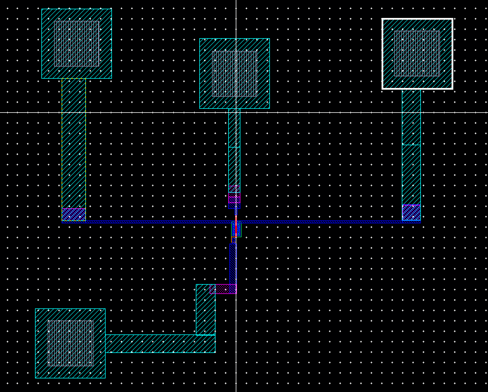
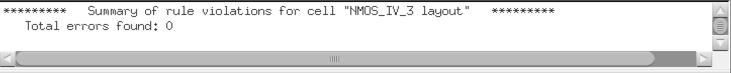
After testing my symbol the next step was to layout my NMOS. Again, the tutorial initially walked as through in the wrong way as a learning experience. In this case, it was connecting our source to the ptap our mos. After laying out I next DRC'd my layout to verify my layout is following all the rules.  
4Extracted View
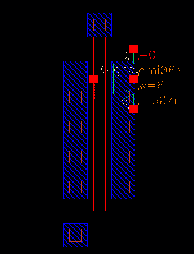
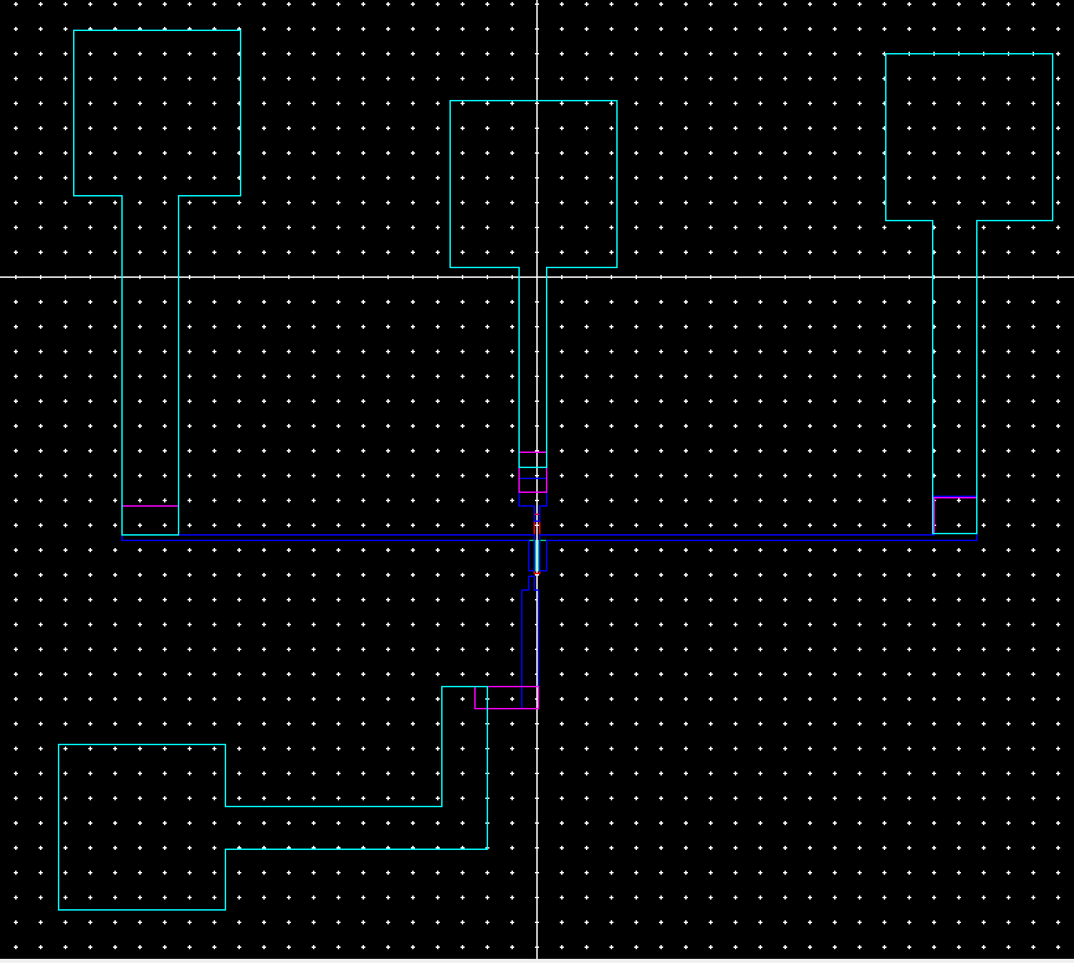
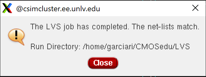
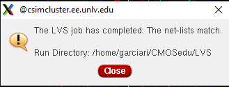
After laying out and DRC'ing my design I next extracted my layout then LVS'd my layout to verify it was correct.
LVS output
5Transisent Response
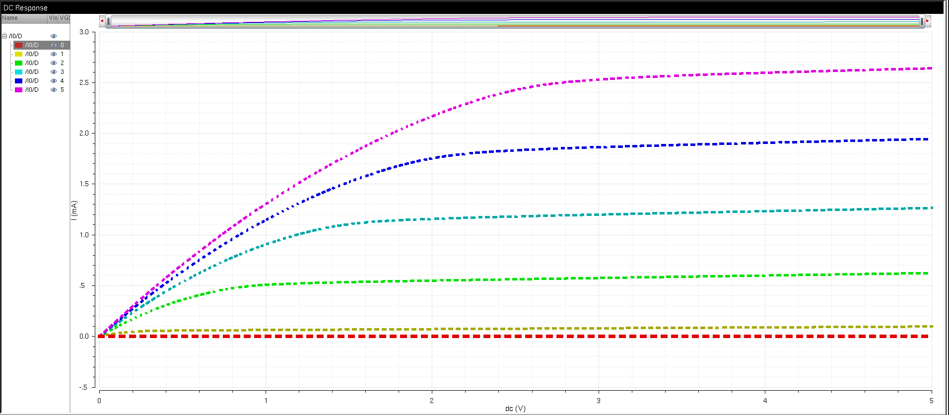
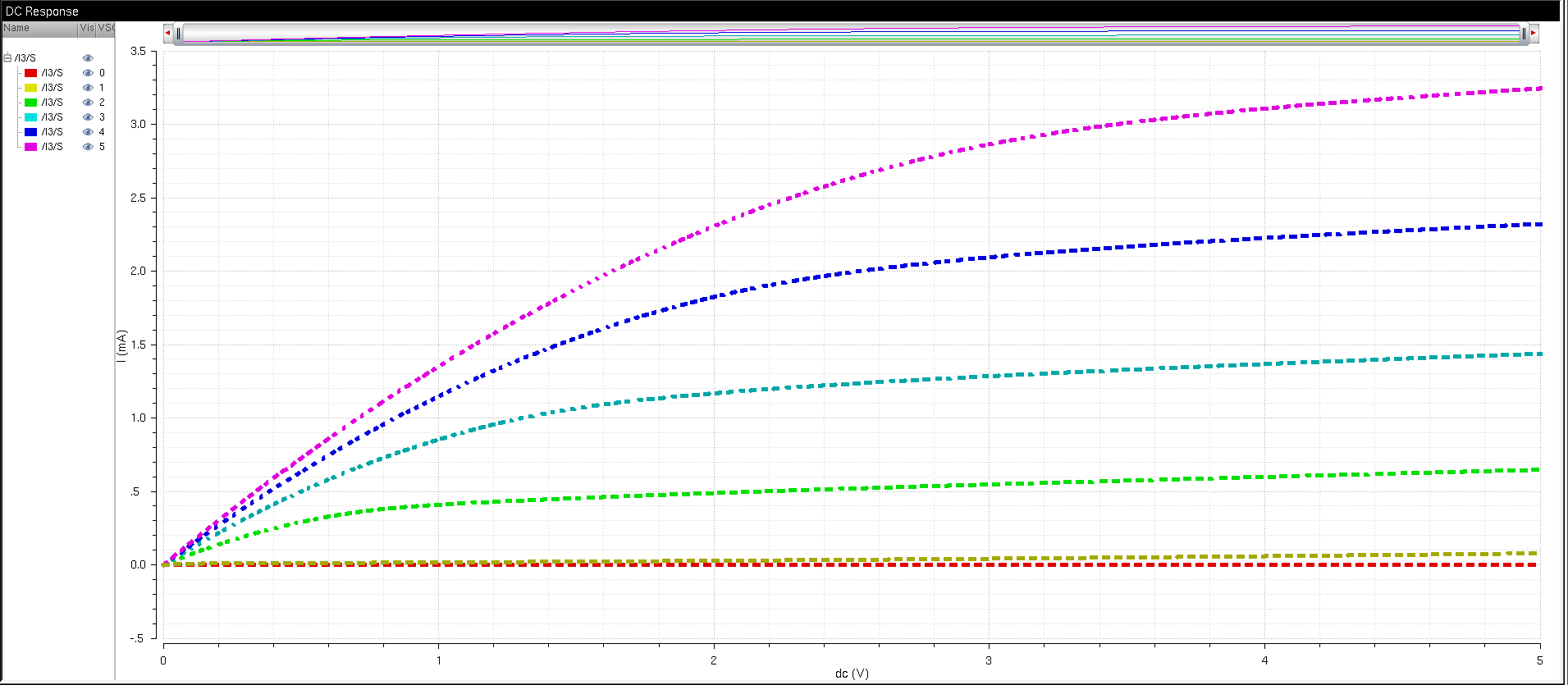
The final step was to re run our simulations but this time editing the settings so that it simulates using my extracted layout. Additionally I outputted my netlist to verify that it was infact using my extracted layout.
Netlist extracted
6Schematic
After completing the nmos layout the tutorial next walked me through the process of laying out a PMOS transistor. Similar to the nmos process we start with creating a schematic. 
7Symbol
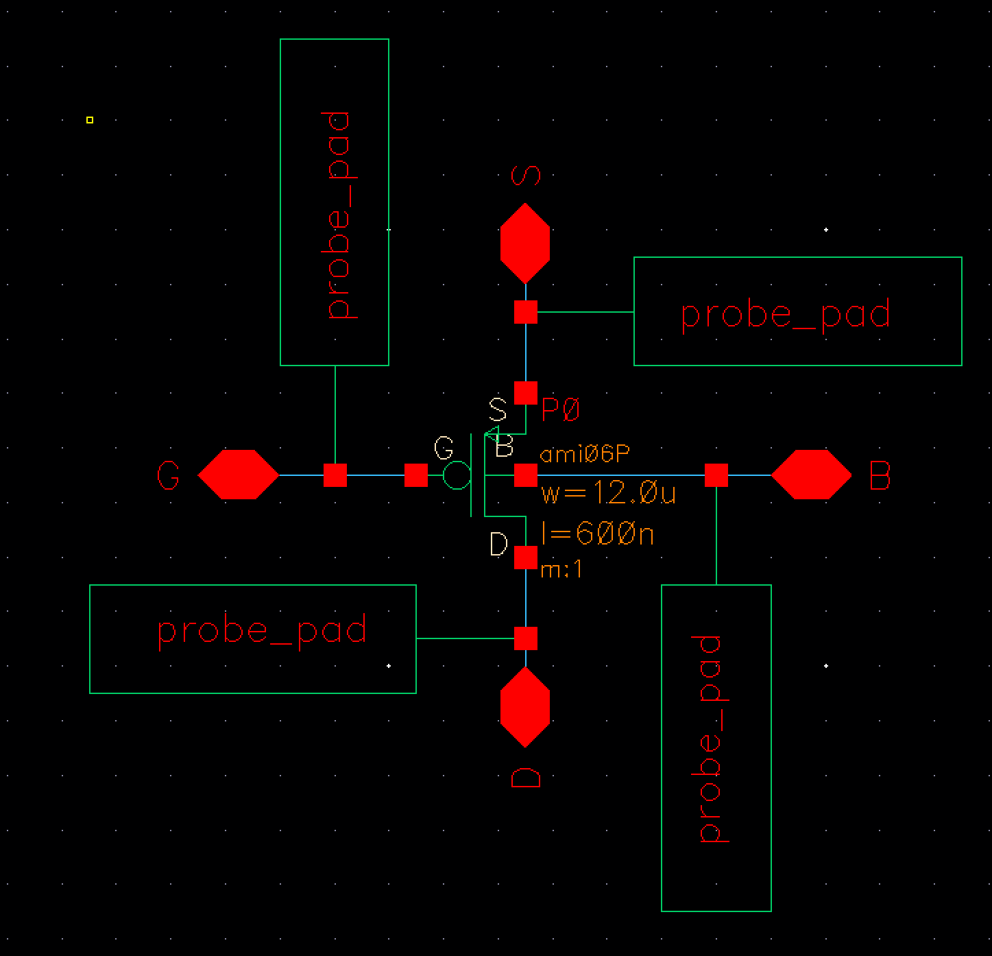
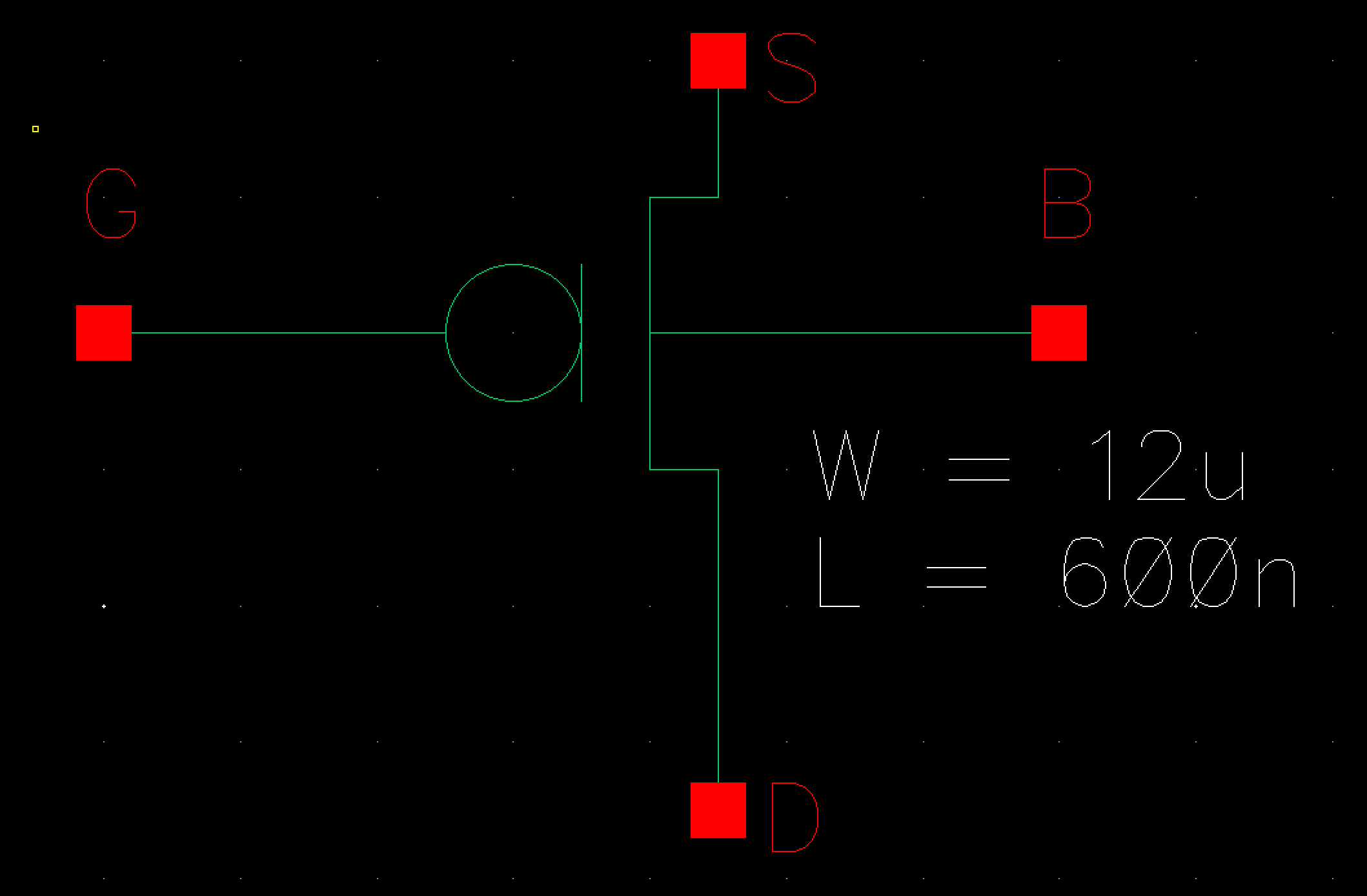
After creating a schematic, I create a symbol view of my schematic in order to simulate and verify that my schematic is working as intended.
Symbol Schematic
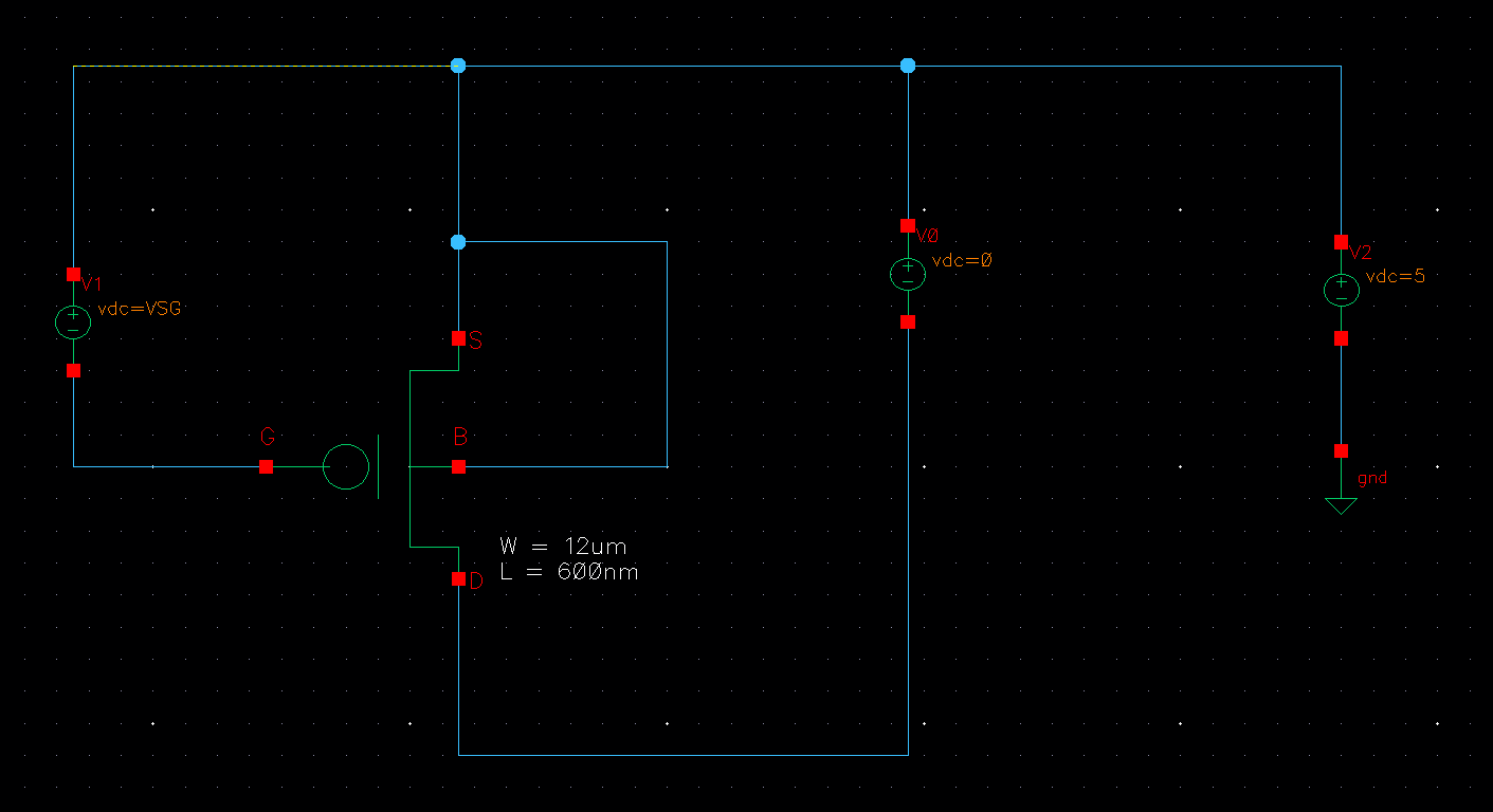
Schematic using my Symbol
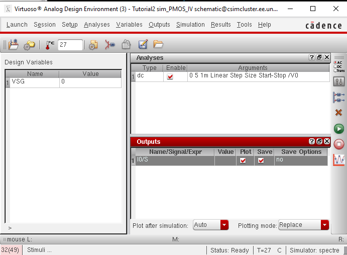
ADE L
ADE L Settings
Transisent Output
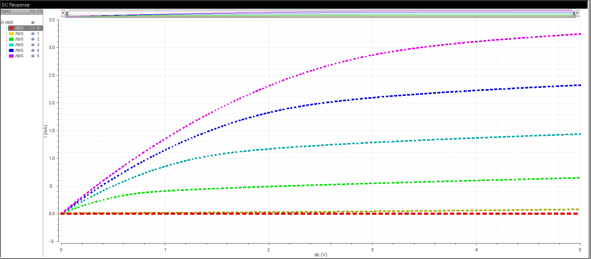
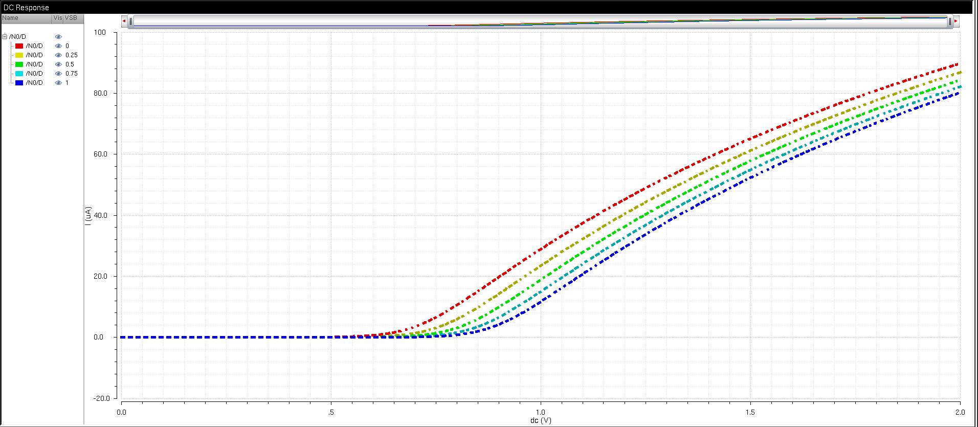
Output of Parametric Analysis
8Layout
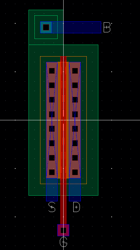
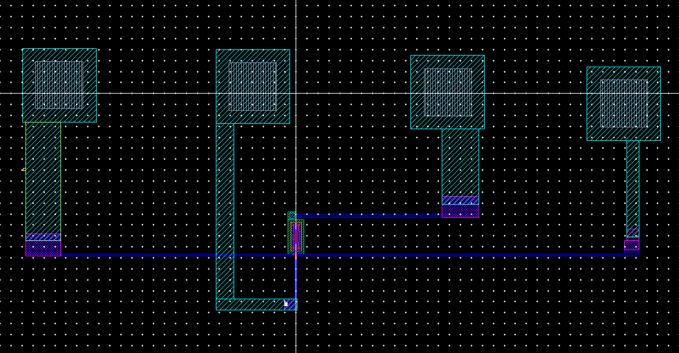
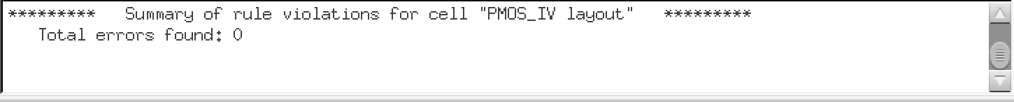
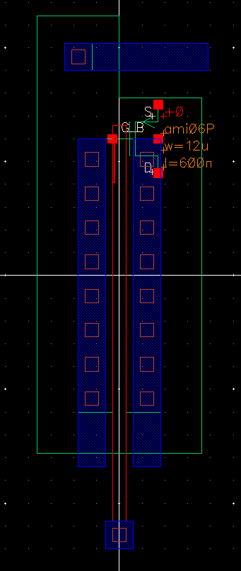
With our symbol successfully simulating I was now ready to move onto laying out. After creating the layout and DRC'ing my layout I created an extracted view of my layout.
Extracted
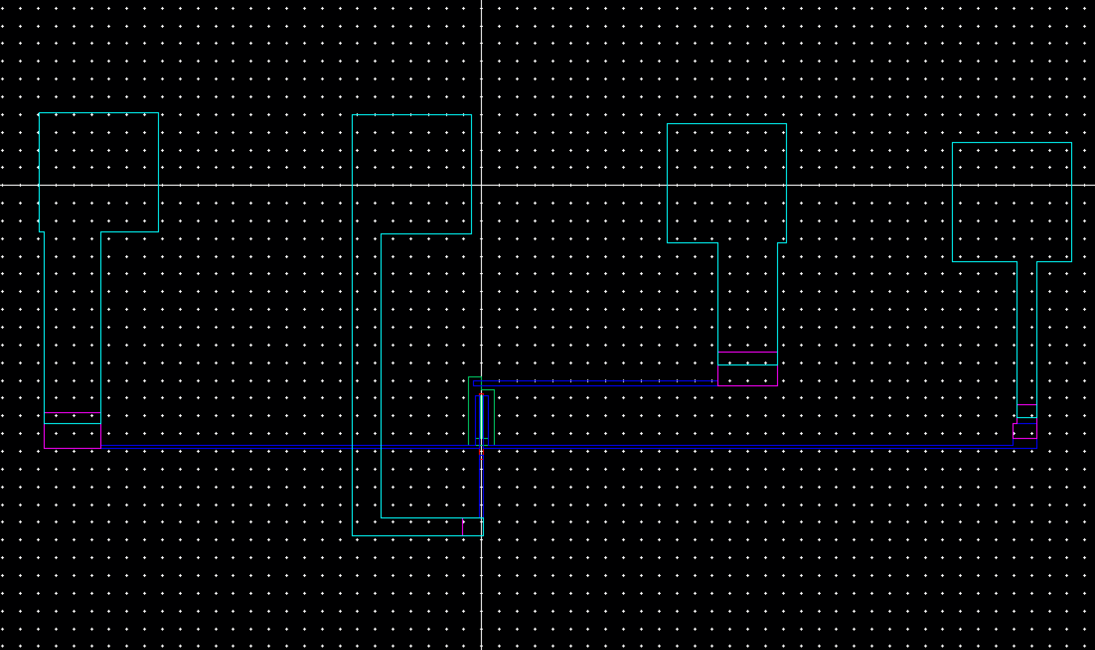
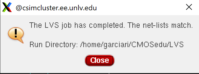
With my extracted view created I proceeded to test my extracted layout by running and LVS and verifying that it is correct.
LVS
9Schematic
With my extracted layout sucessfully passing LVS all that was left to do was to simulate a pmos circuit using my extracted layout.
ADE L
Similar to the NMOS simulation I had to edit the settings to tell ADE to simulate using my extracted view.
Transisent Analysis
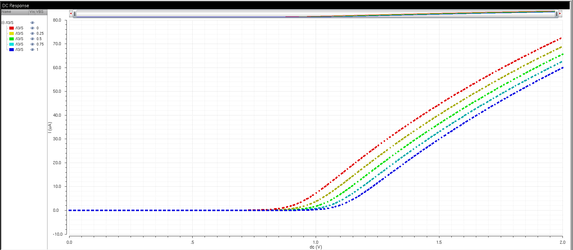
Our output matches our initial schematic simulations.
Extracted ADE
Once again verifying that our simulation is in fact using our extracted view.

 Lab

1The first part of this lab was to run through various simulations to see the effects of VSG, VSD, VGS, and VDS on the current that flows through our MOS transistors.
VDS
ID vs VDS(NMOS 6u/600n)
ID v VGS
ID vs VGS(NMOS 6u/600n)
ID vs VDS
ID vs VSD(PMOS 12u/600n)
ID vs VSG
ID vs VSG(PMOS 12u/600n)
2Schematic
Next I was tasked with designing another NMOS again like the prelab but this time it would be connected to probe pads. Like above before we can layout our nmos I must first create a schematic of my NMOS. As seen above this schematic is same as NMOS except for the addition of probe pads to all pins.
Symbol
I next created a symbol of my NMOS.
Layout
After creating my symbol I next moved onto creating a layout of my NMOS. Again it was similar to the prelab layout however this time I had to account for the addition of the probe pads. After laying out I DRC'd my layout to confirm it was properly layed out.
DRC
After verifying DRC, I next extracted my layout.
Extracted
After extracting my layout, I run an LVS to make sure my layout is correct.
LVS
I have successfully layed out a 6u/.6u NMOS transistor with Probe Pads
3PMOS Schematic
The final part of this lab was to repeat the 2nd part but this time with a PMOS transistor this time. As with the PMOS prelab, I begin by creating a schematic of my PMOS but with the addition of probe pads. After creating my schematic, I next created a symbol of my schematic.
PMOS Symbol
After creating my symbol I was now ready to move onto laying my PMOS with the additional probe pads.
PMOS Layout
The layout process was the same except for the addition of the probe pads. After creating my layout I verified that followed DRC rules.
DRC
With my laying out successfully passing DRC all that was left to do was extract my layout and verify LVS.
Extracted
LVS


Return to EE 421L Labs