Lab 3 - Layout of a 10-bit digital-to-analog converter(DAC) ECE 421L
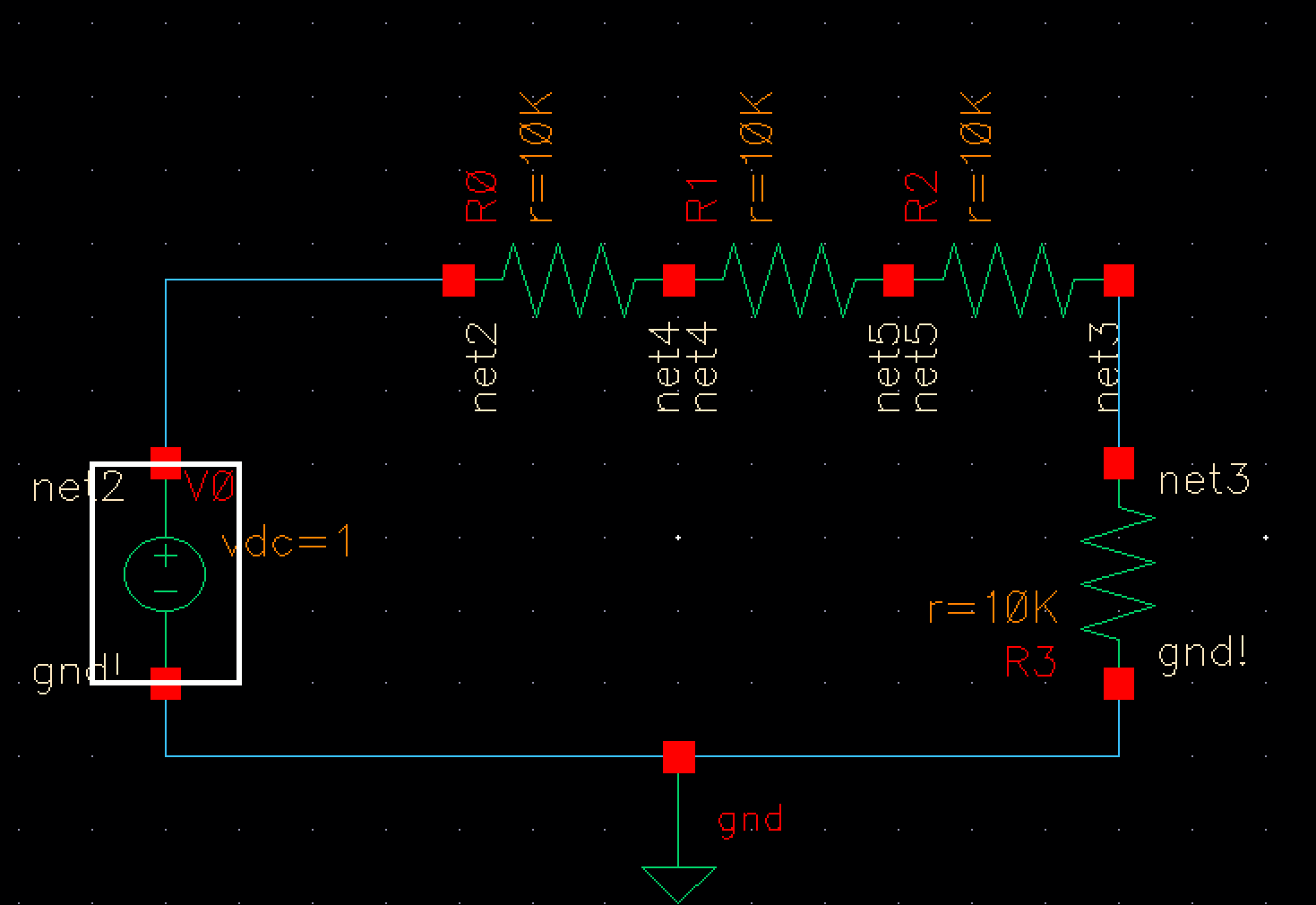
| 1 | 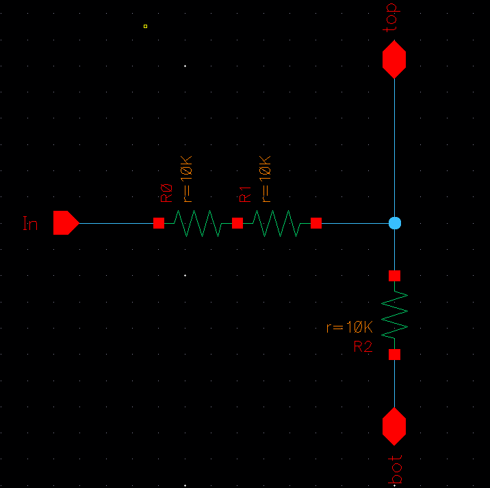 The first step of this lab was to create the base schematic for designing a 10bit DAC. I achieved this by creating a schematic that contains 1 input 2 input/output pins. This schematic provides the basis for our DAC and allows for a simplified design. We will use this design 10 times in our DAC once per bit. After completing schematic I drc'd to ensure that no errors were made. 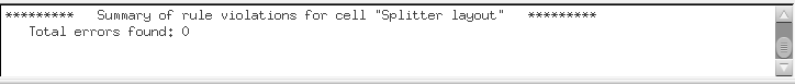 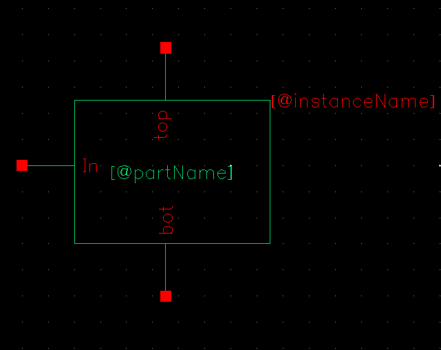 After designing I created a symbol so that we can move onto connecting all of these symbols and creating my DAC. |
| 2 | 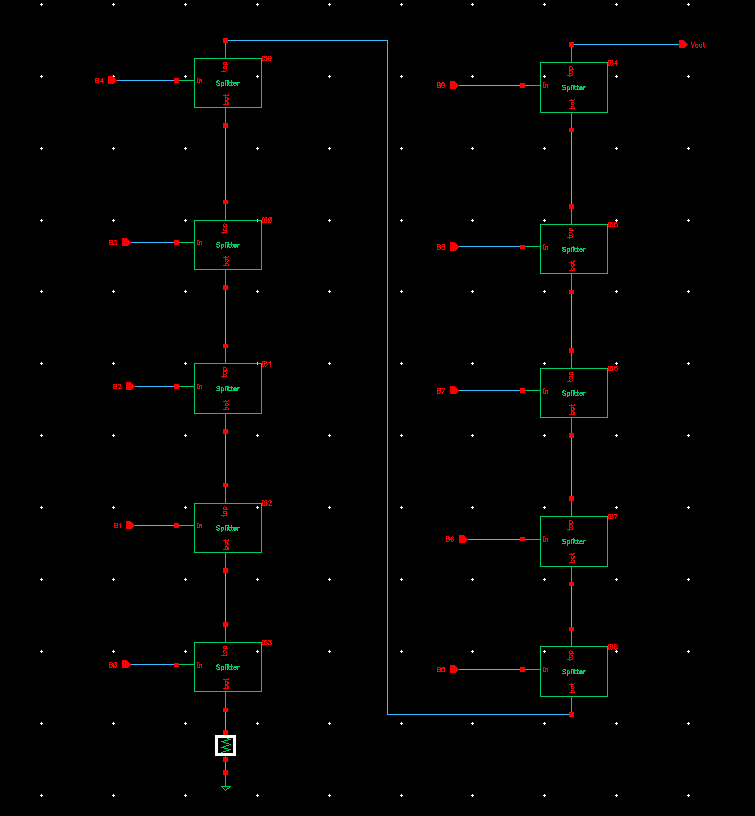 In this step I had to use my previously created symbol to create my 10 Bit Dac. I copied the already existing 10 bit DAC design so that I wouldn't have to edit symbol size to get it to fit in the ADC to DAC schematic. After implementing my symbols for each bit I next had to add an additional resistor in bit 0 as well as a ground. After completing this schematic I drc'd the schematic to ensure no errors were made. |
| 3 | 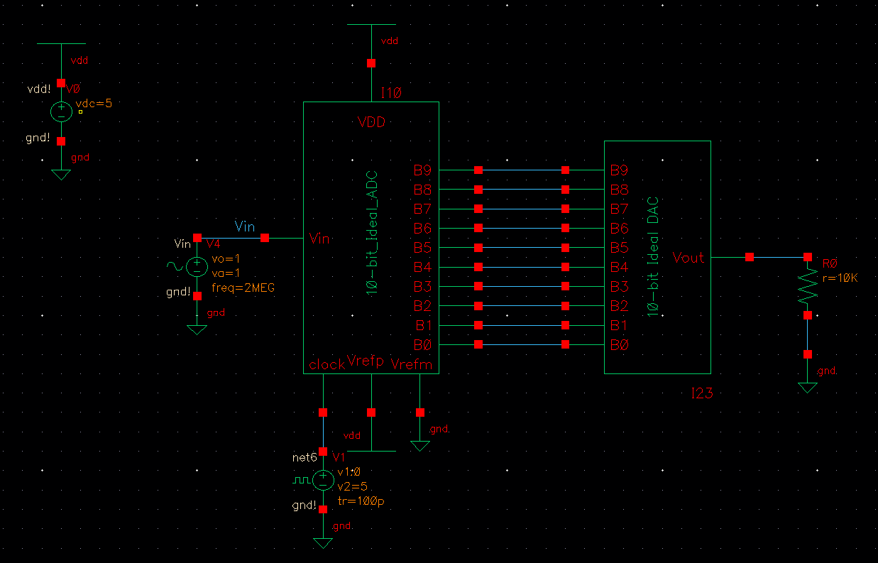 After successfully creating 10 Bit DAC I next extracted the symbol for my 10 Bit DAC and then ran a simulation using my DAC to make sure that my design worked. It did. 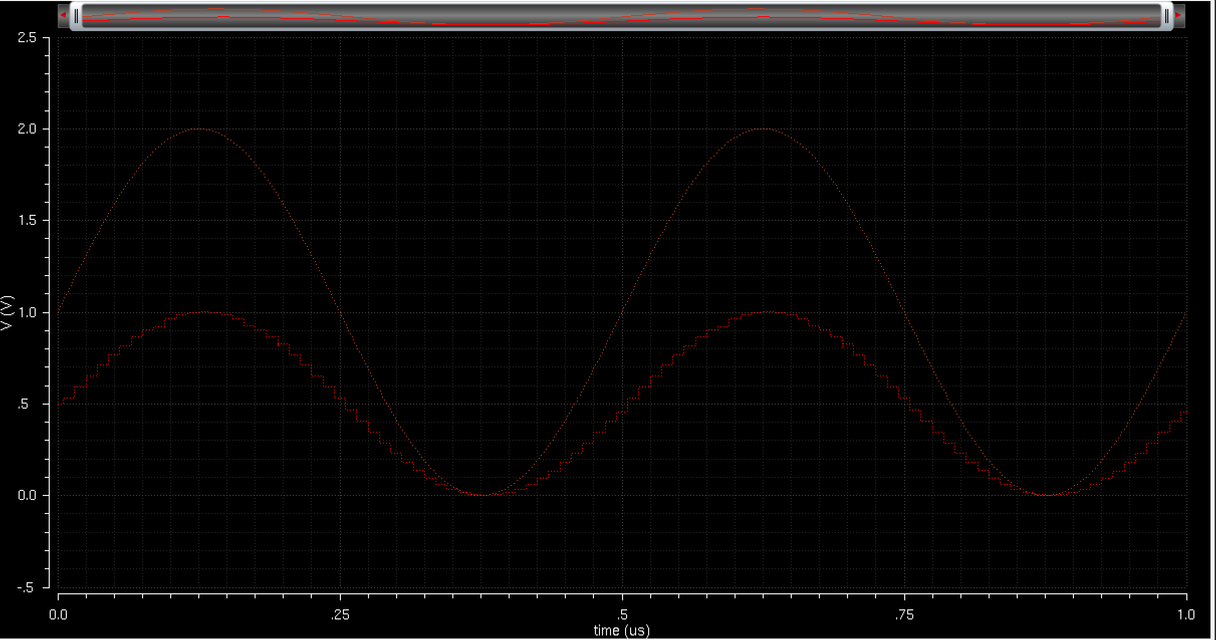 |
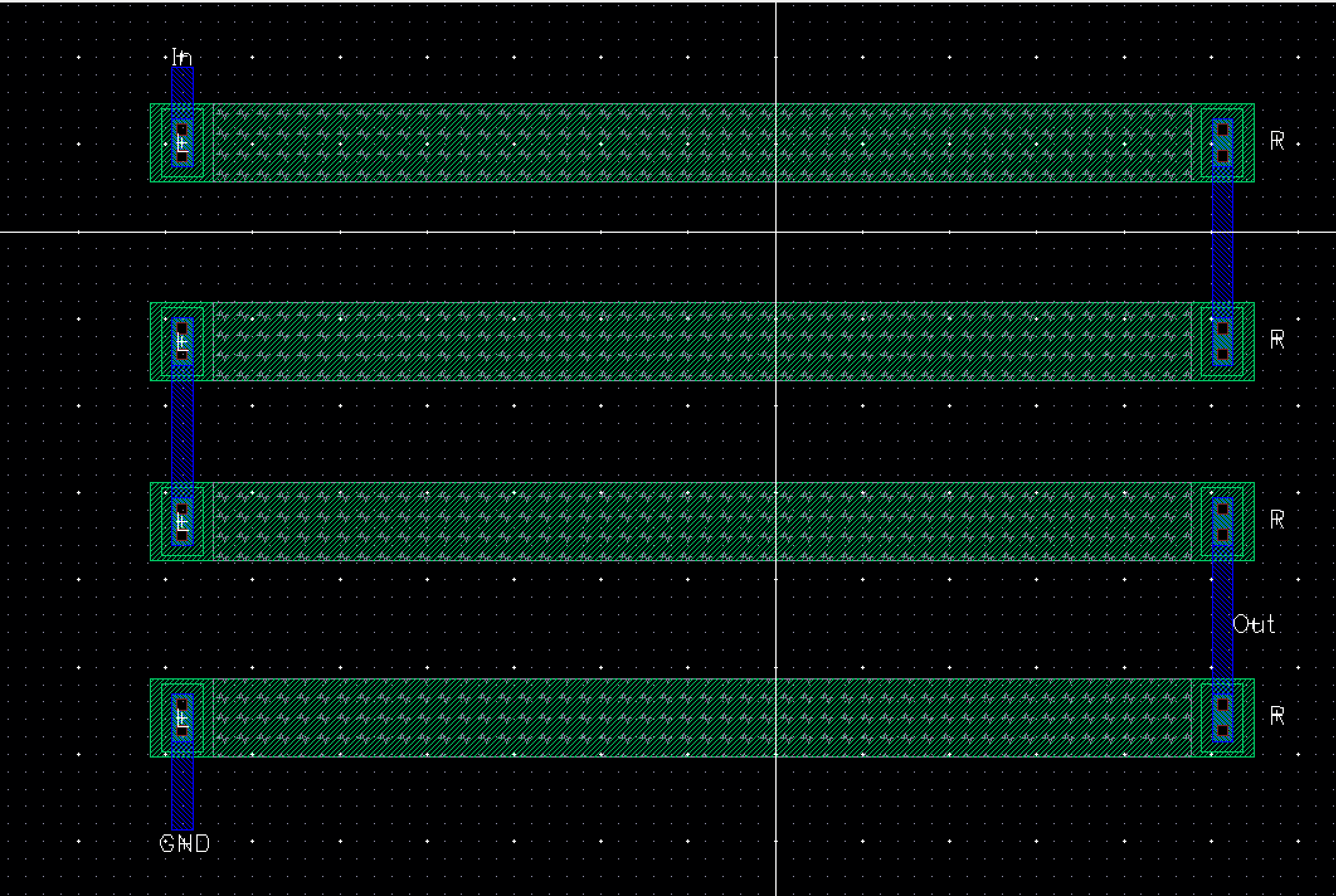
| 4 | 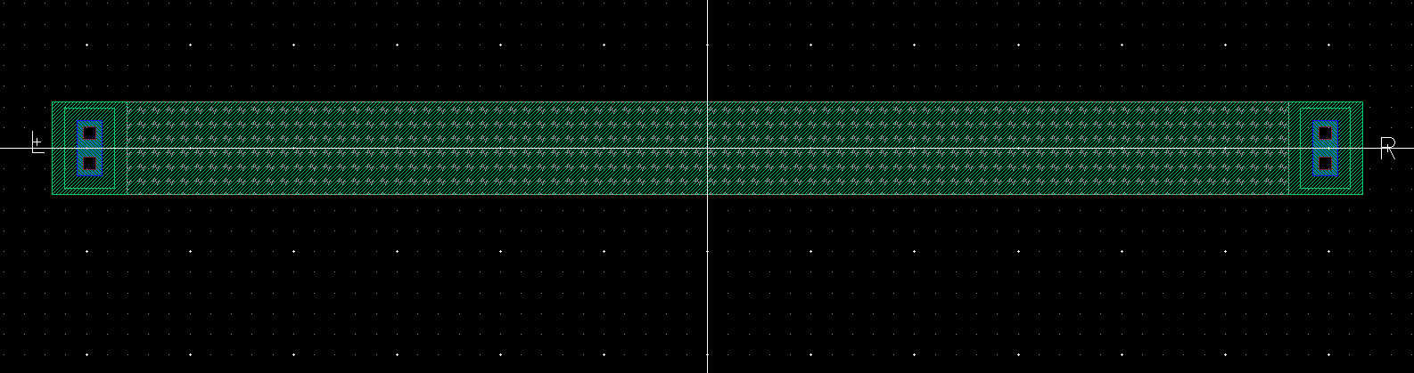 Since everything worked well I can now move on to creating the layout of my 10 Bit DAC. I first had to create a 10k n-well. After creating the layout for my 10k nwell I had to extract the layout to ensure my design was correct and indeed did have 10k resistance. 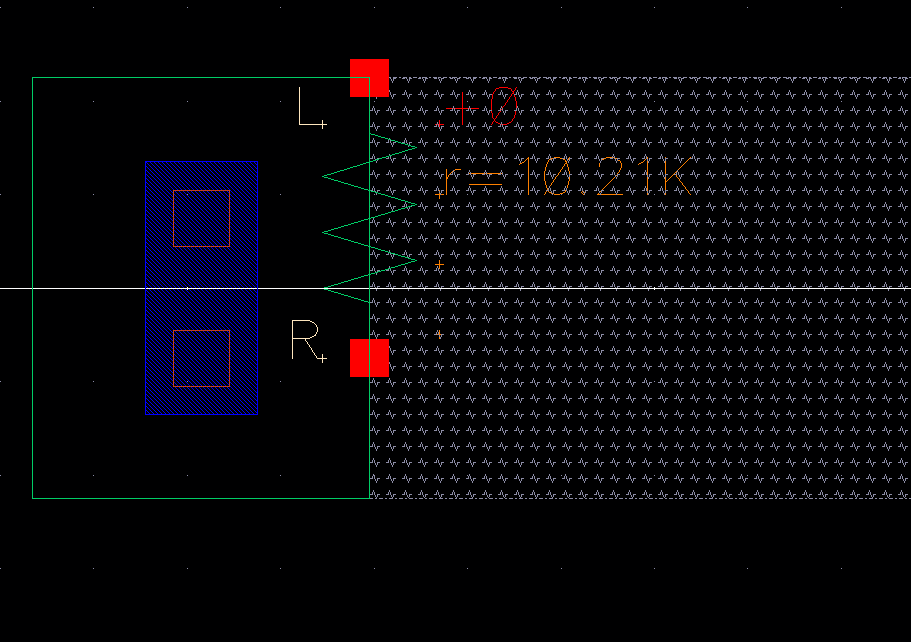 |
| 5 | 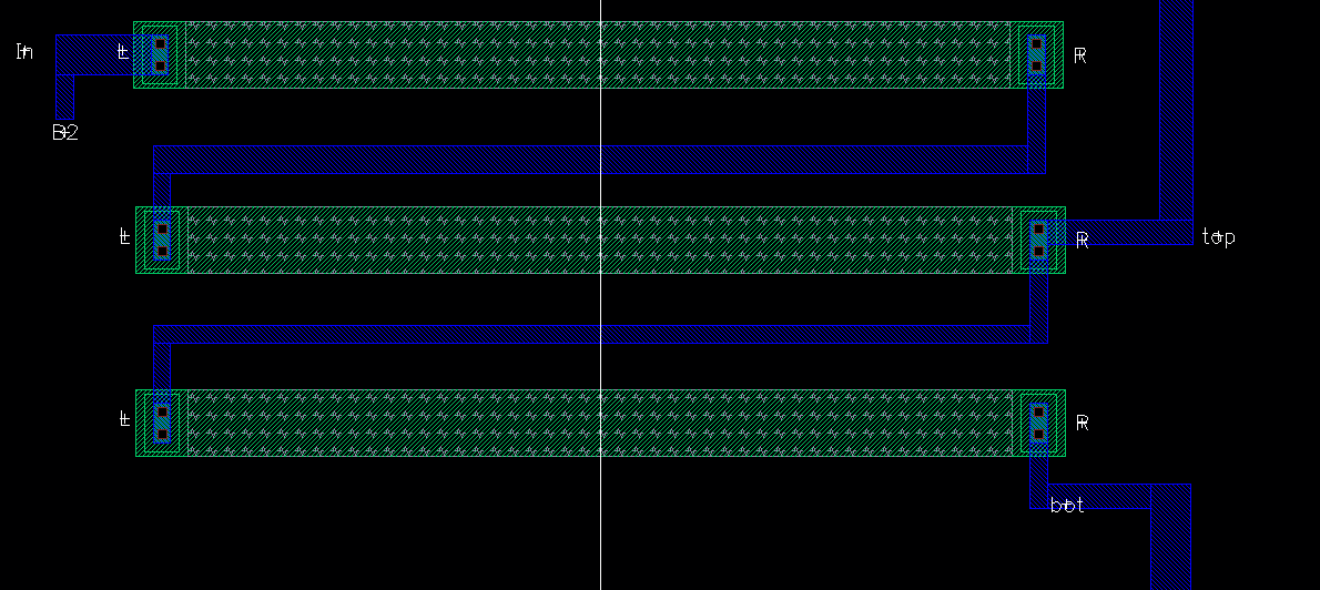 After successfully laying out my 10k n-well resistor I next moved onto laying out my bit symbol. This was achived by stacking 3 resistors on top of each other. The first resistor takes in the bit controller input, the second resistor functions as the resistor in series with the input resistor and the third resistor takes in the input from a lower level. I also added 3 pins an in, bot, and top bit. |
| 6 | 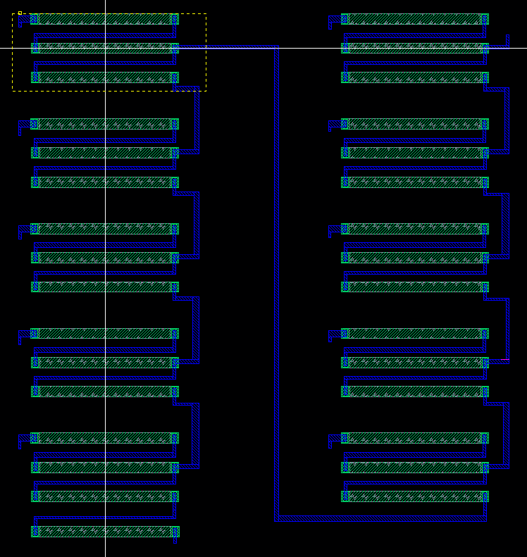 After laying out the bit resistors I could finally move onto laying out my 10 bit DAC. This was simple since I designed my 10 bit dac in modules so all I had to do was instantiate 10 of the bit layouts and connect them in the right manner. An additional step I had to perform was adding pins for the inputs that denote which bit is coming into my resistor. Before I began to layout my bit layouts I had to make sure that were layed out in an ordered manner. To ensure this I had denoted a constant x-position as well as how much lower each next bit should be. I decided that each bit layout should be 45um apart from each other.(Measured from the origin of each layout) I drc'd my layout to make sure that no spacing errors were made or no loose metal connections existed. 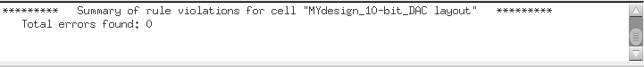 After orderly laying out my bit layouts and making all the right connections all that was left to do is test the LVS. 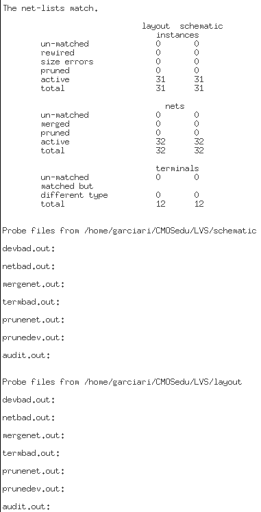 LVS passed successfully and I had successfully layed out my 10 Bit Dac. |