| 1 | 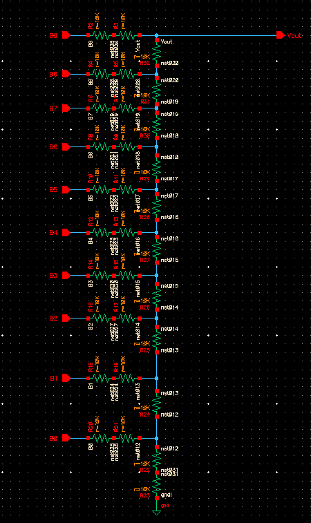
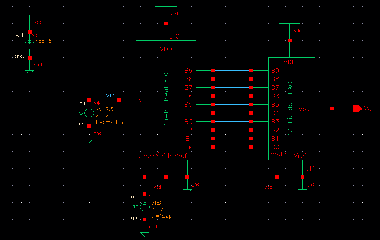
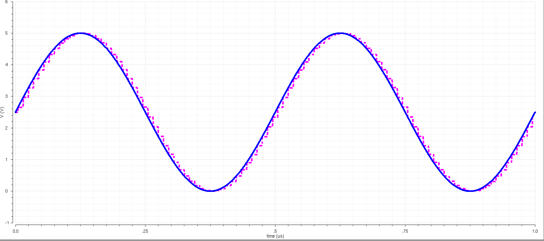
Part 1 of the lab was to design a DAC using figure 30.14 as a guide. I designed my DAC by using 10k resistors. |
| 2 | 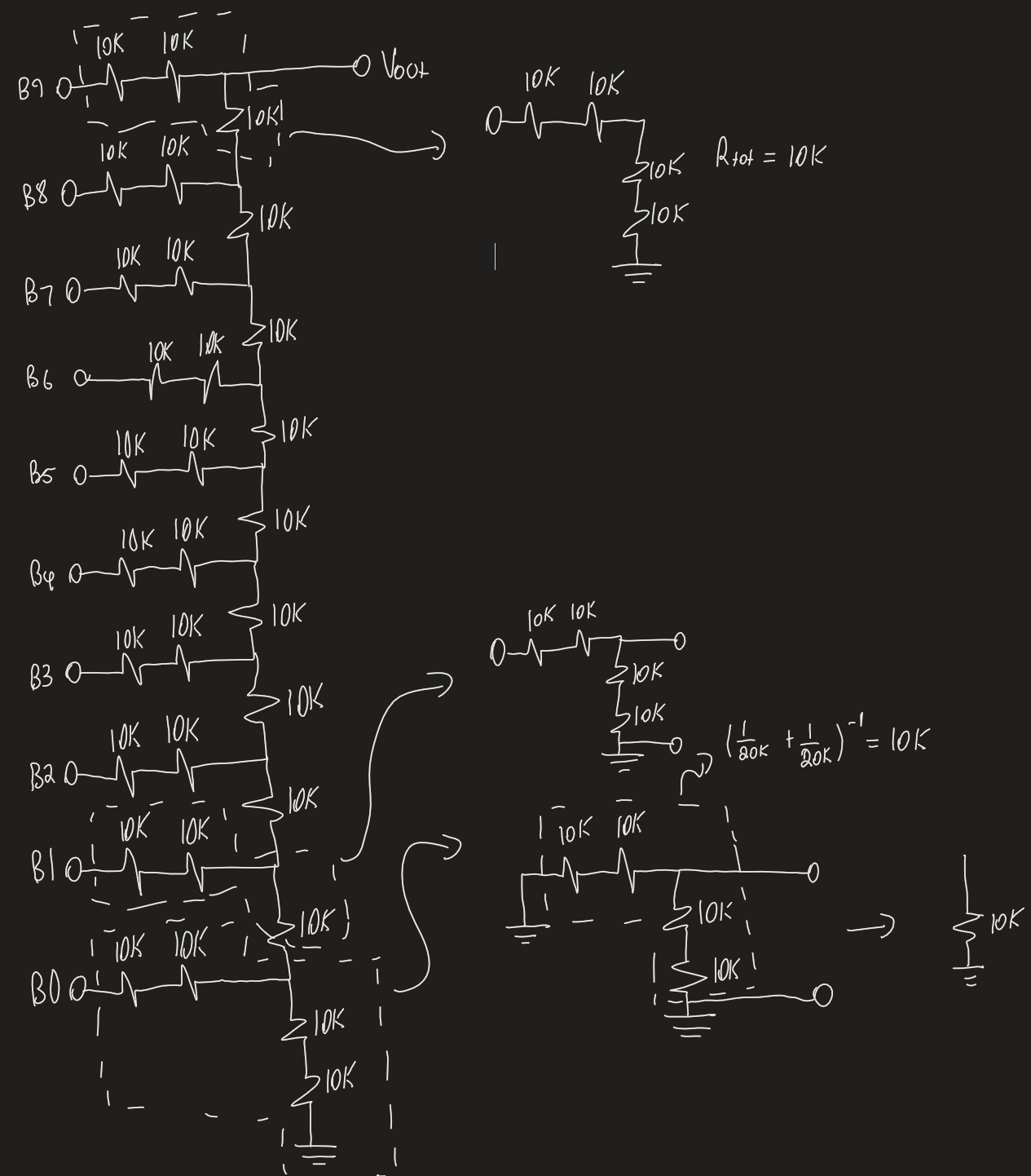
Part 2 of the lab asked me to determine the total resistance
of my DAC. I achieved by grounding all inputs to my bits and then doing
repeated thevin simplication until I obtained the final total resitance
of 10K. |
| 3 | 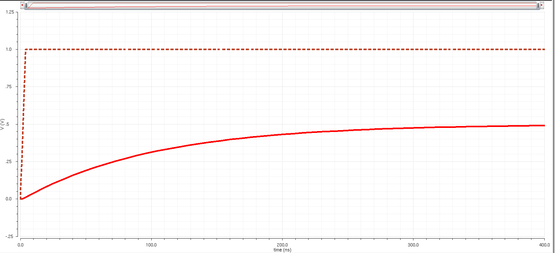
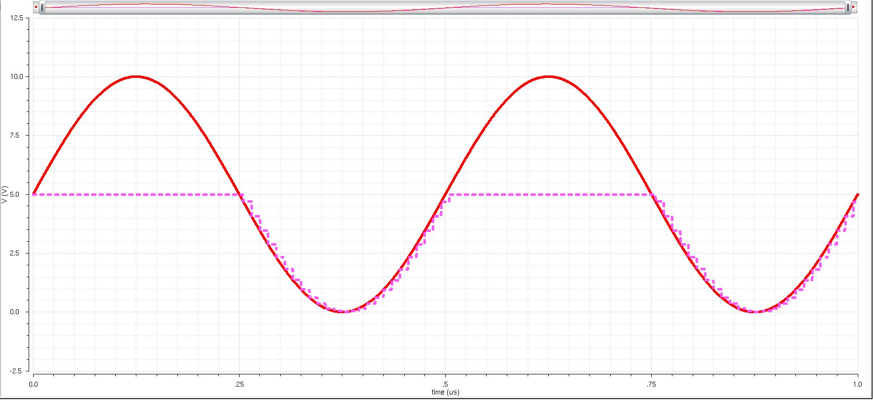
Part
3 of the lab asked me to ground all my bit inputs except for the most
significant bit(B9), add a pulse voltage source, then add a 10pF
capacitor as load. I then simulated the circuit and performed hand
calculations afterwards to confirm the results of my simulation. For my
hand calcutions I obtained .7*(40k)*(10p) = 280ns approximately matches
my simulation results. |
| 4 | 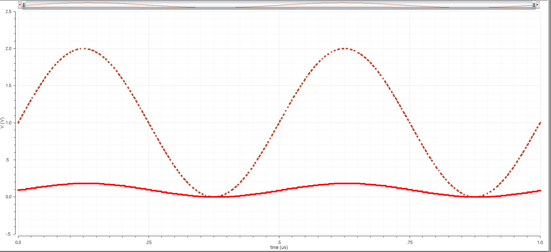
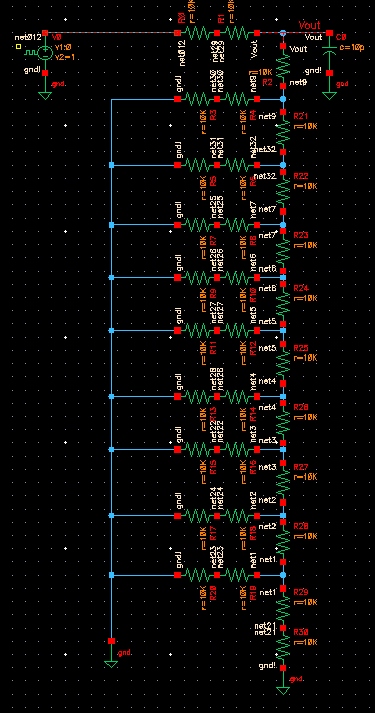
Part
4
of the lab was when I finally got to implement my DAC into the original
ADC to DAC schematic. I did this by first making a copy of the original
DAC design. After copying I first edited the symbol view to remove VDD,
VERFP, and VREFM since they will no longer be used and leaving them in
the symbol will just produce errors. Once I did this I next moved on to
creating my design in the copy DAC schematic after creating my
schematic I then clicked check and save to make sure that there was no
errors and luckily there were not any errors. After this I created a
copy of the ADC to DAC schematic then replaced the DAC in that
schematic with my DAC then ran transisent analysis to confirm that my
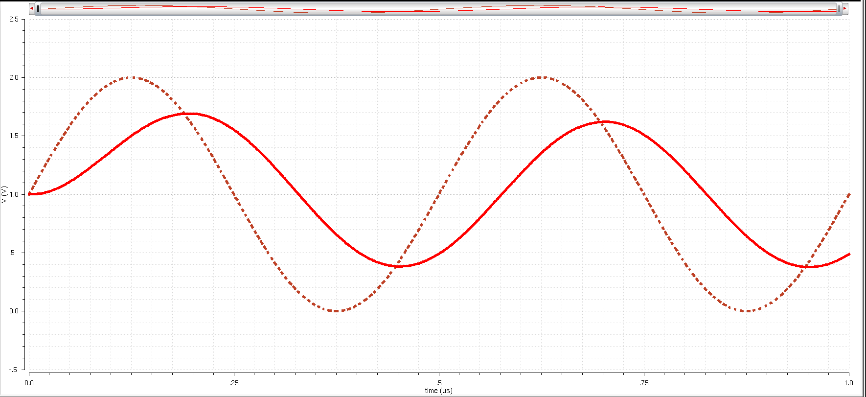
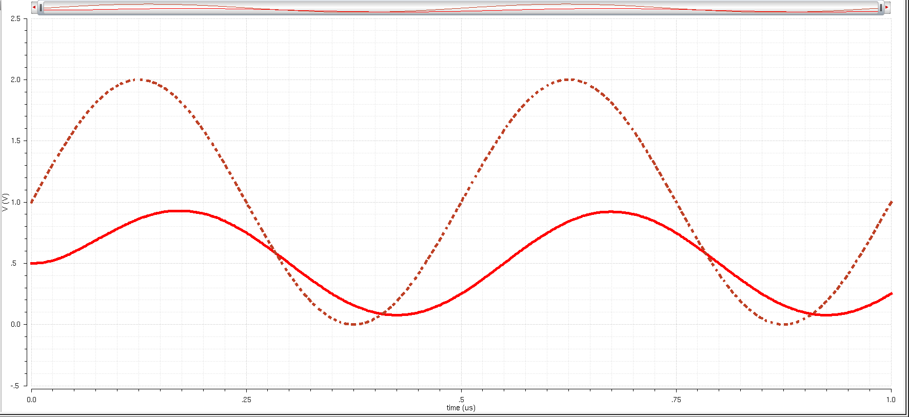
design worked. I next ran simulations using 10K load(Screenshot 1),
10pF load(Screenshot 2) and finally a 10K and 10pF load(Screenshot 3).
If you drive a 10K load, since the total resistance of the DAC is 10K
the circuit ends up becoming a voltage divider. |
| 5 | What happens if the resistance of the switches isn't small compared to R?
If
the resistance of the switches are not small compared to R our output
would be reduced since we aren't accounting for the fact that the
losses produced by the resistance of the switch are no longer
negligible since the resistance of the switch is no longer small
compared to R. This loss would occur at every bit since each bit input
relies on switches. |