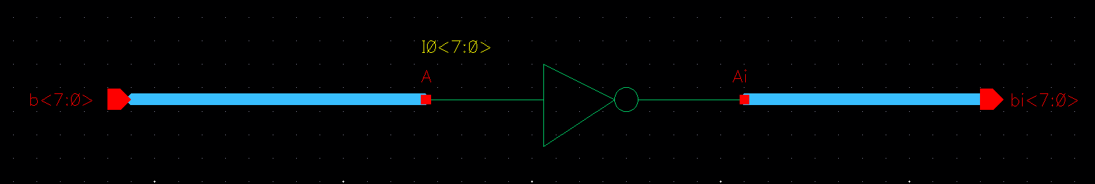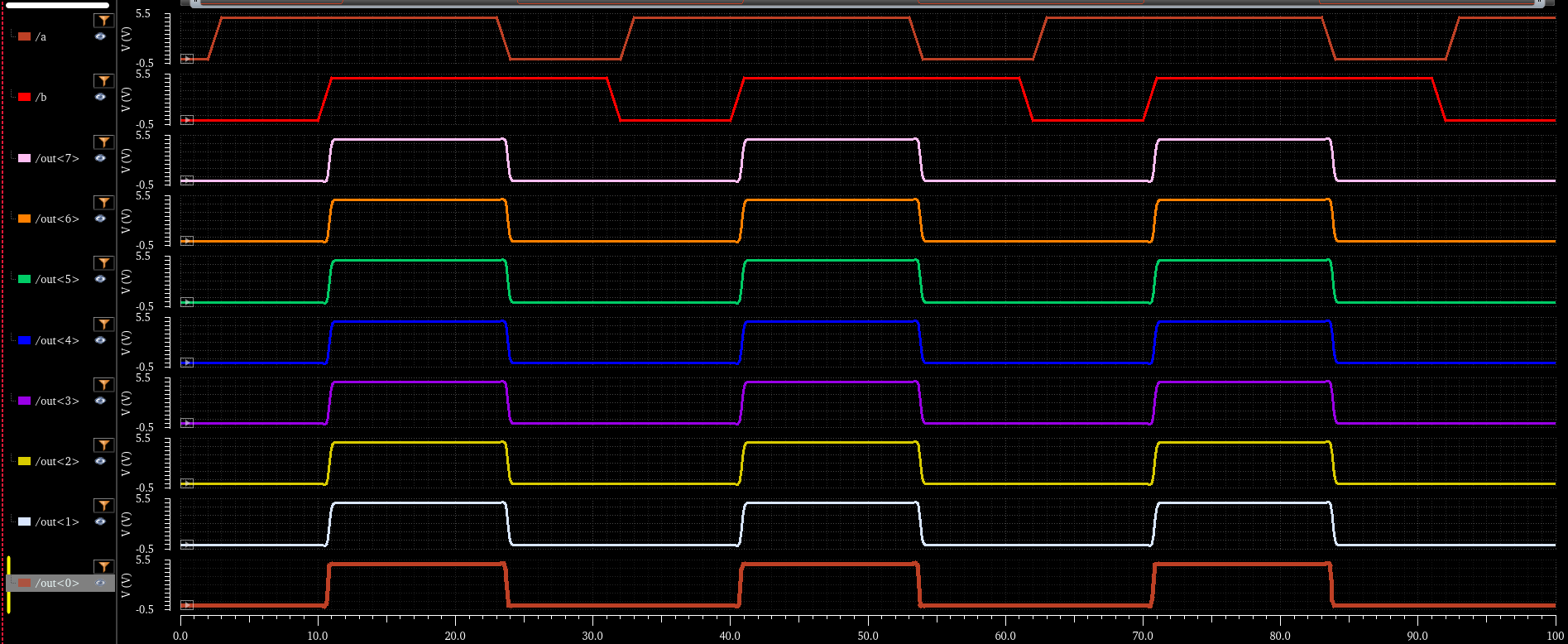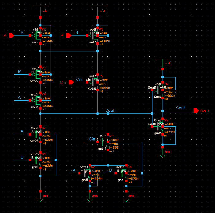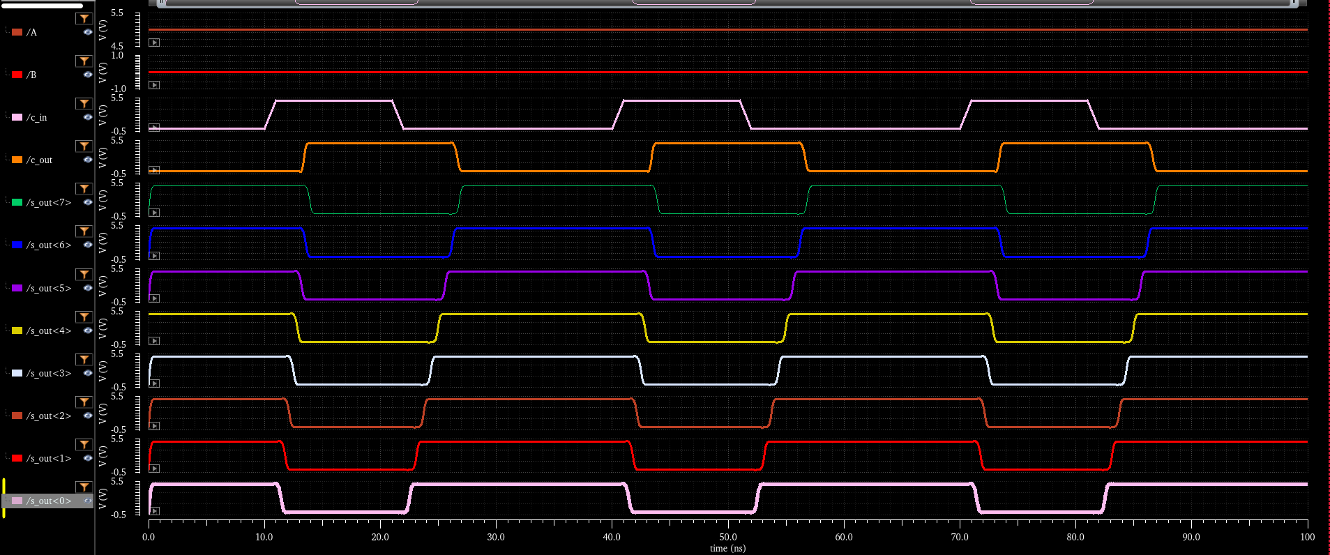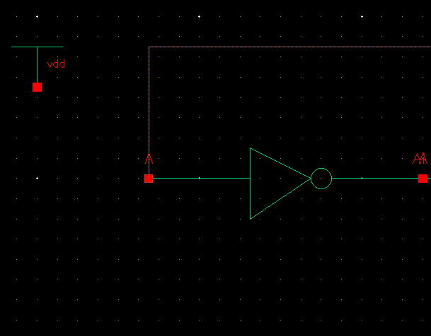
First inverter
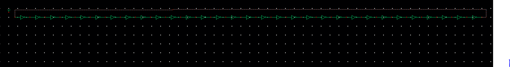
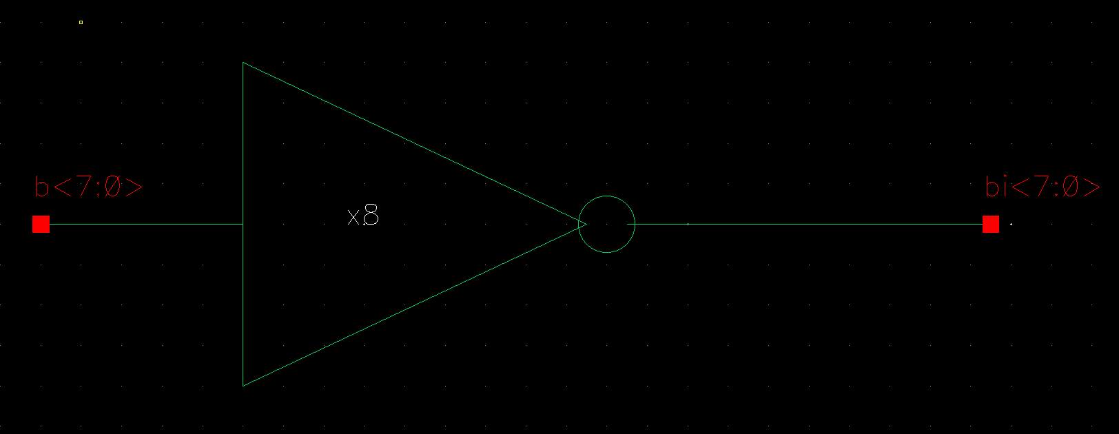
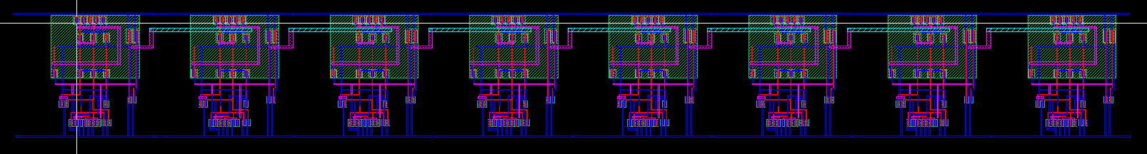
All 31 Inverters
For the prelab I was tasked with completing tutorial 5 which explains the concept of buses and arrays within cadence. The tutorial walks through creating a ring oscillator schematic, symbol and layout in order to explain buses and arrays. The first step of the prelab is to create the schematic of a 31 stage ring oscillator which is done by creating a string of 31 inverters each one feeding into the next.
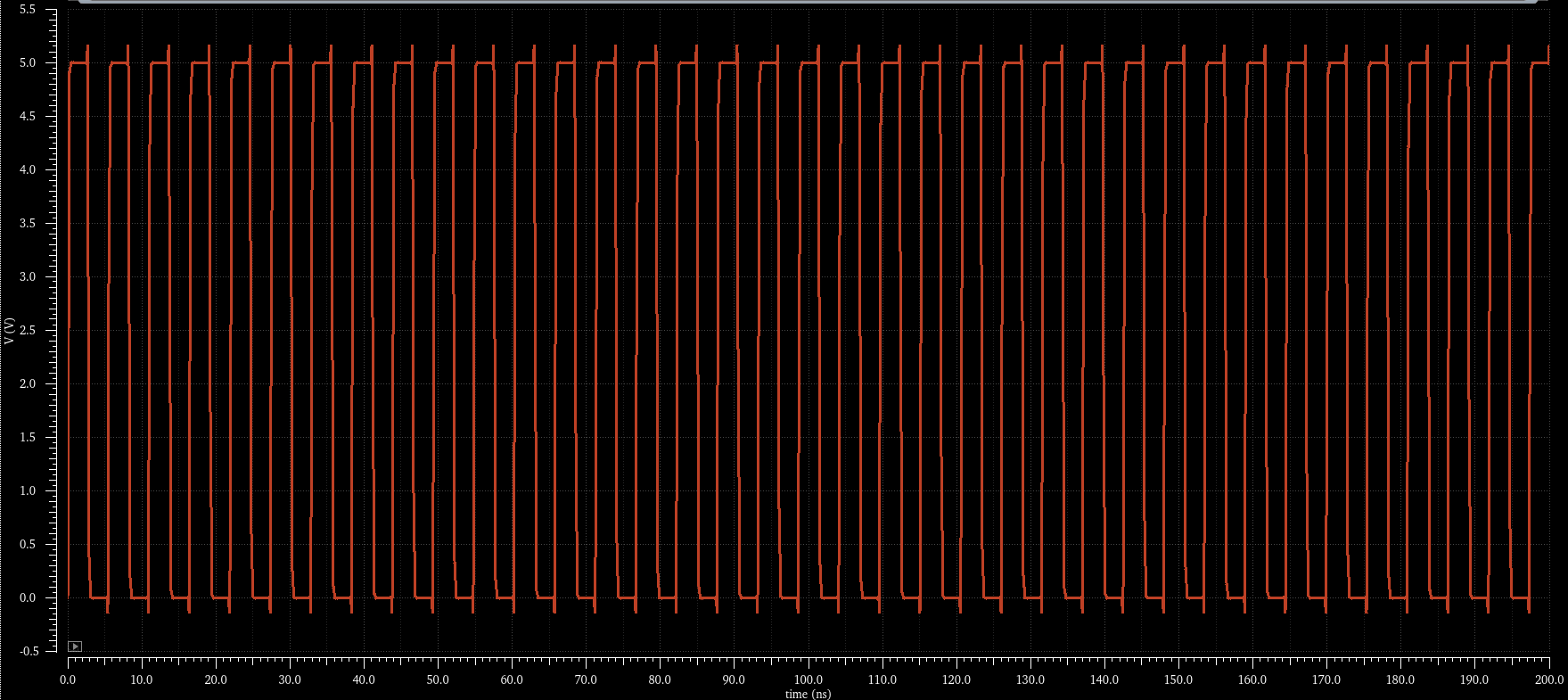
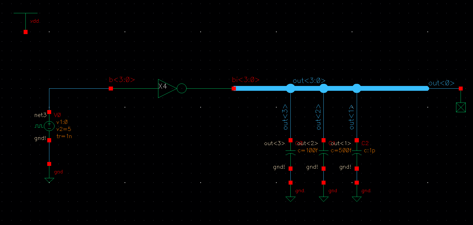
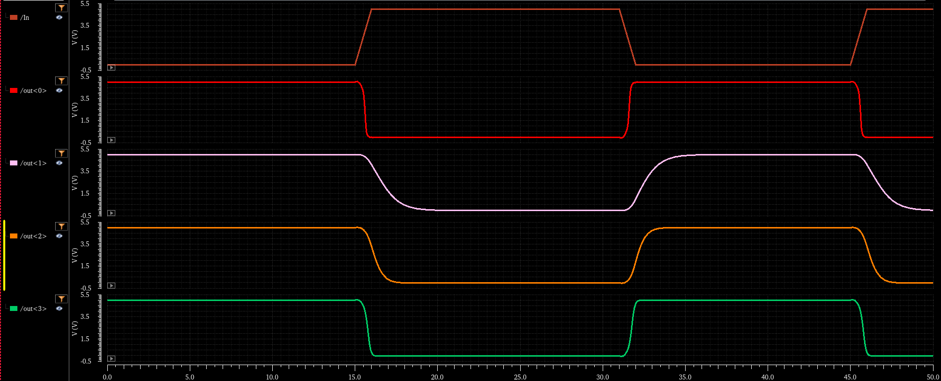
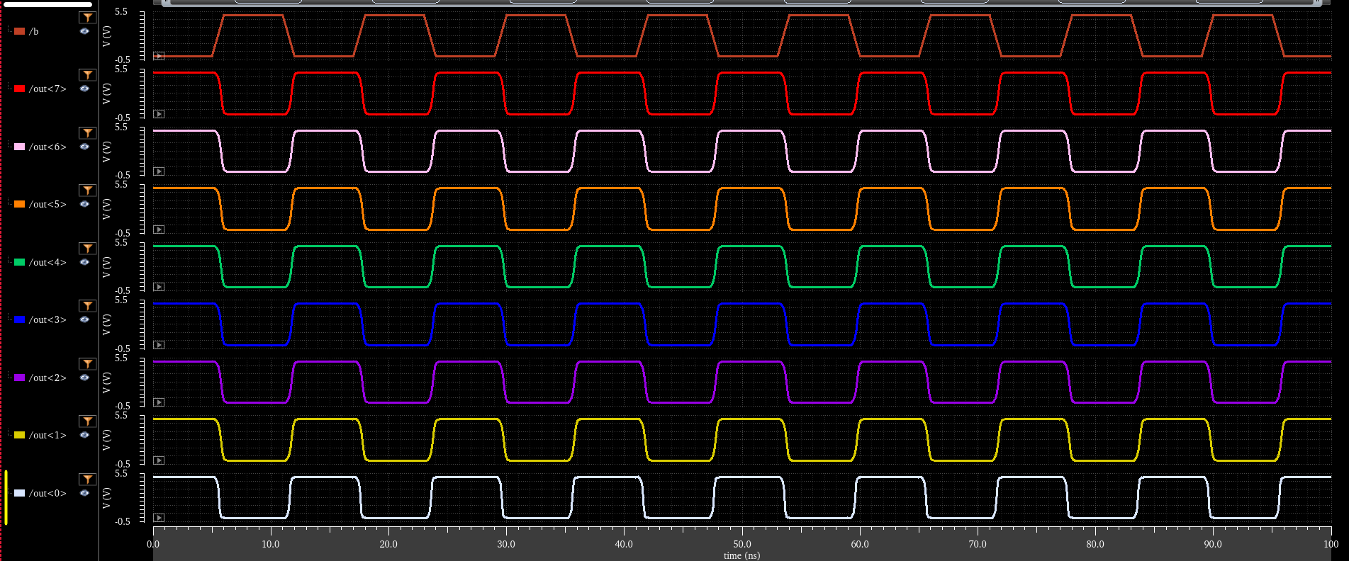
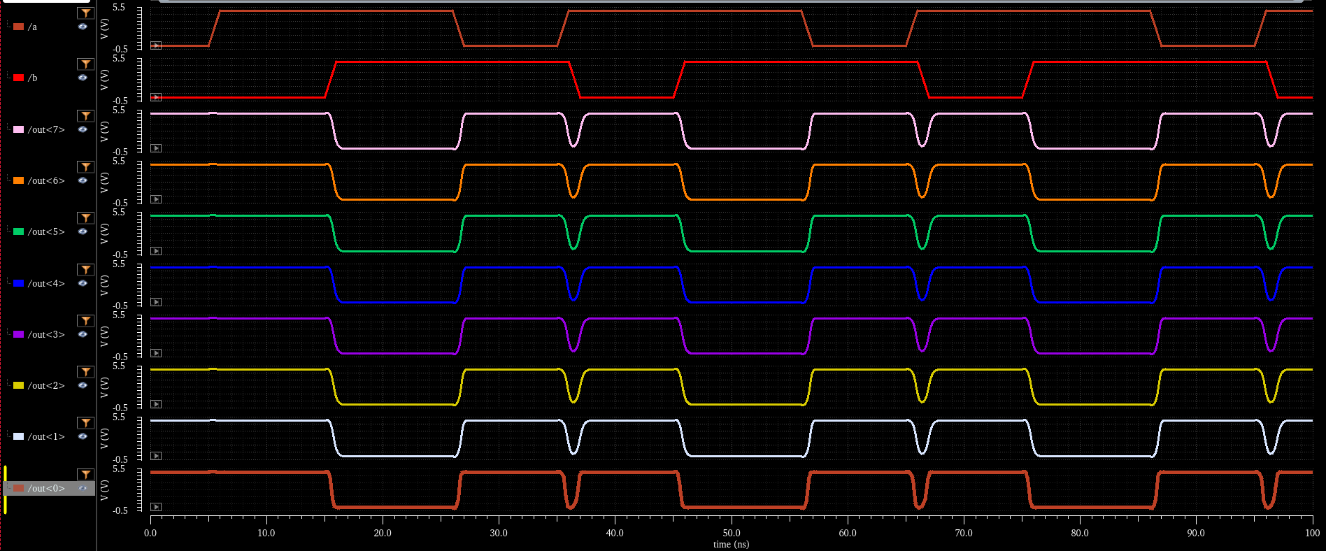
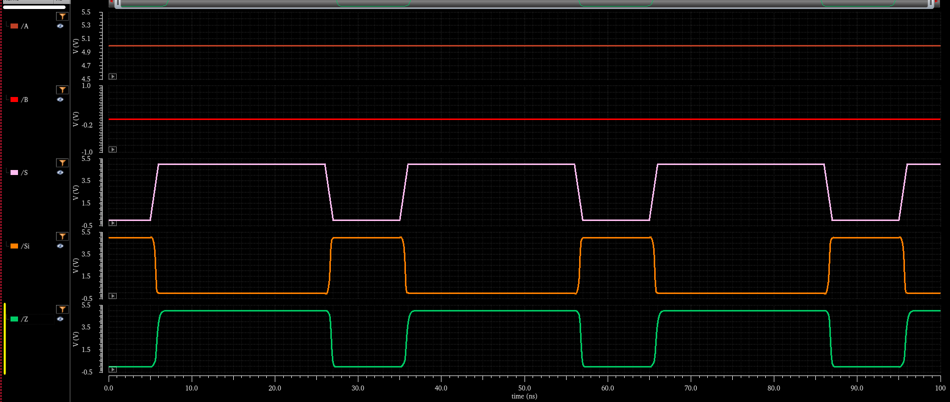
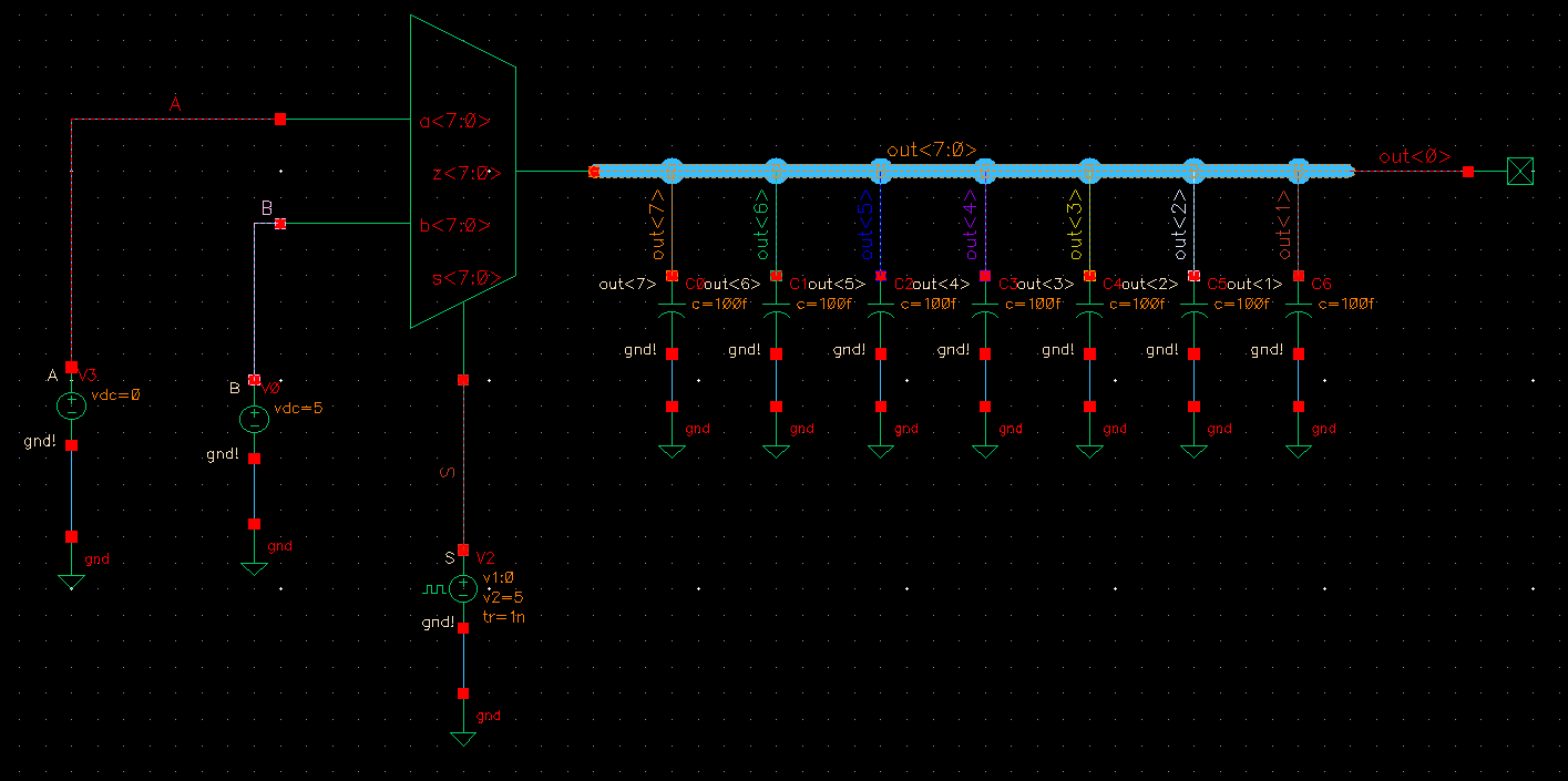
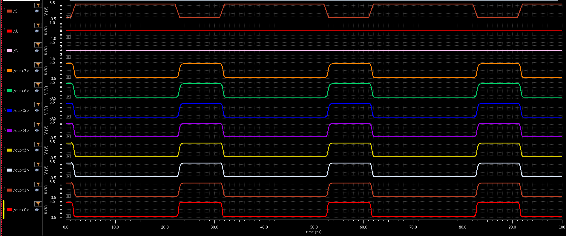
After creating the schematic I ran a simulation of the schematic to see the output of the 31 stage ring oscillator.
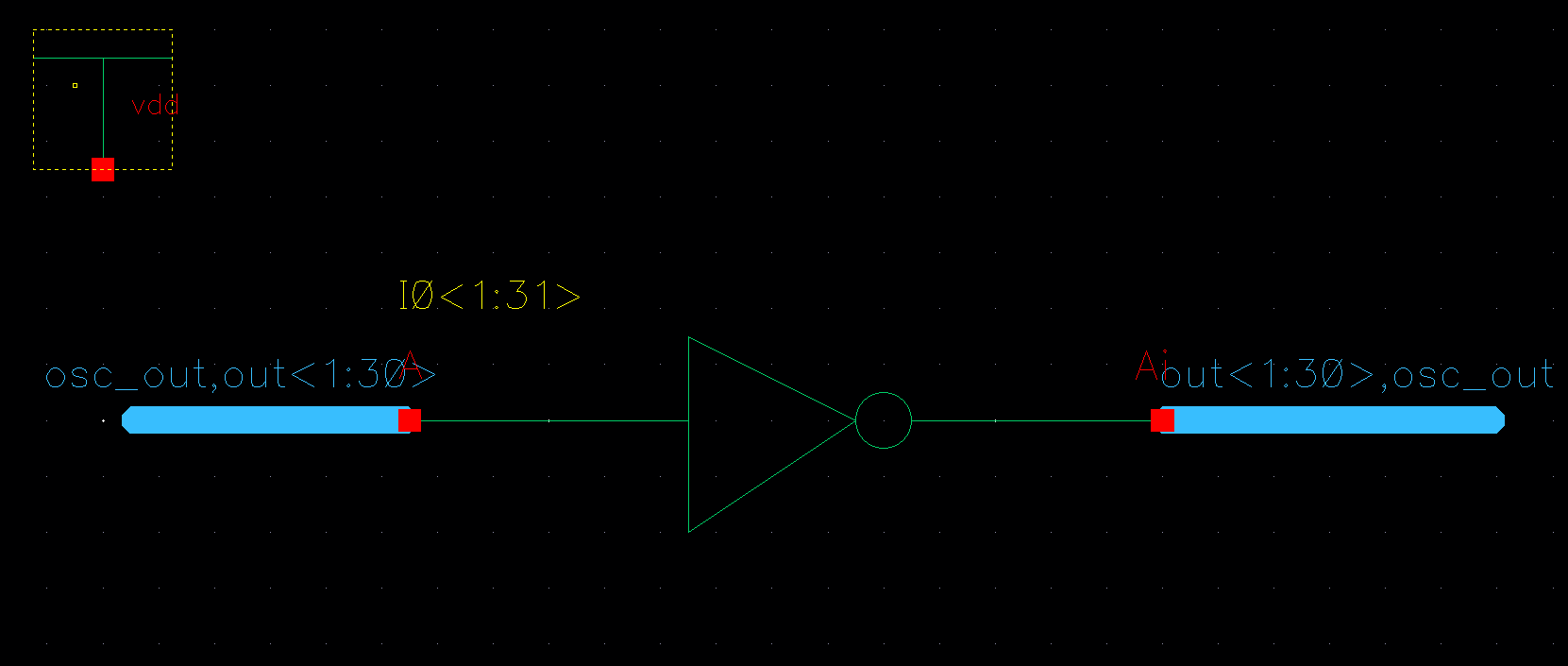
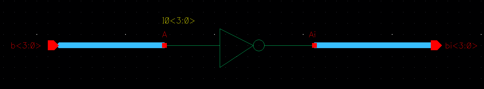
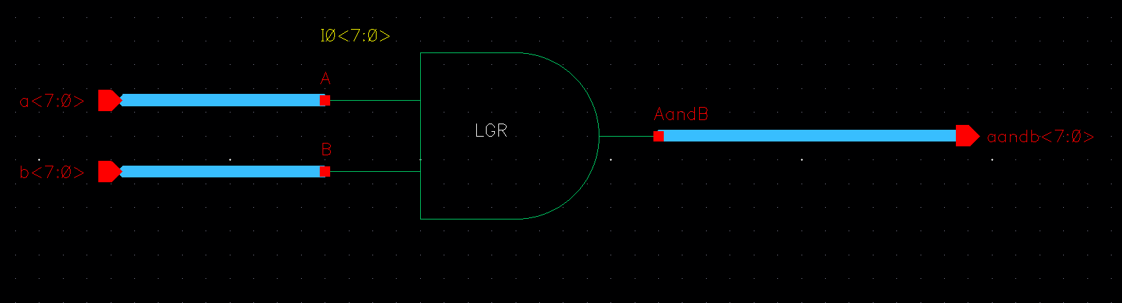
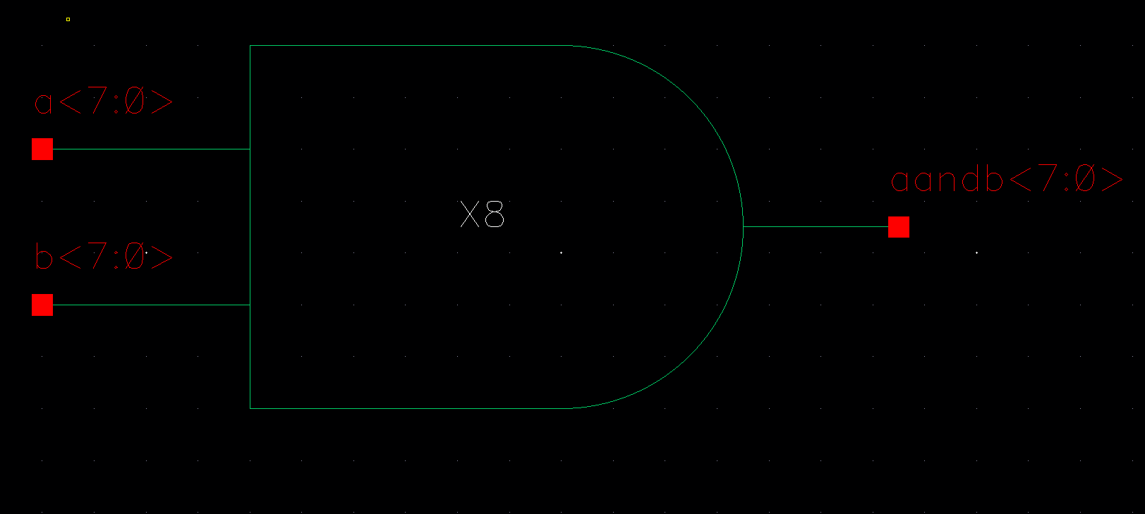
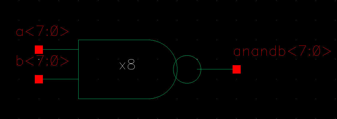
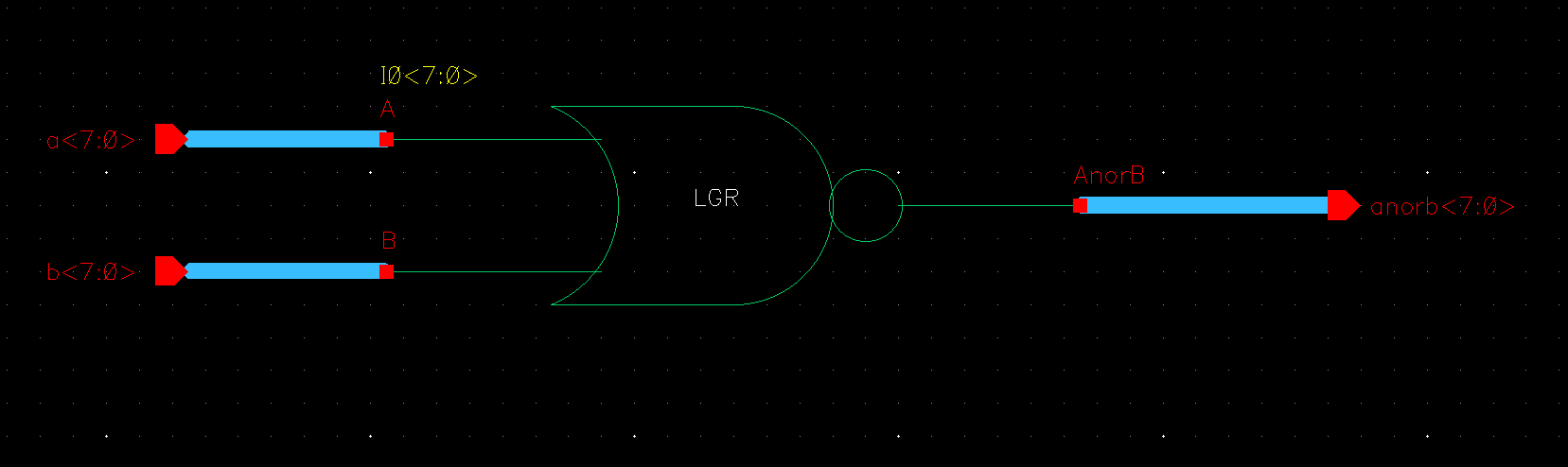
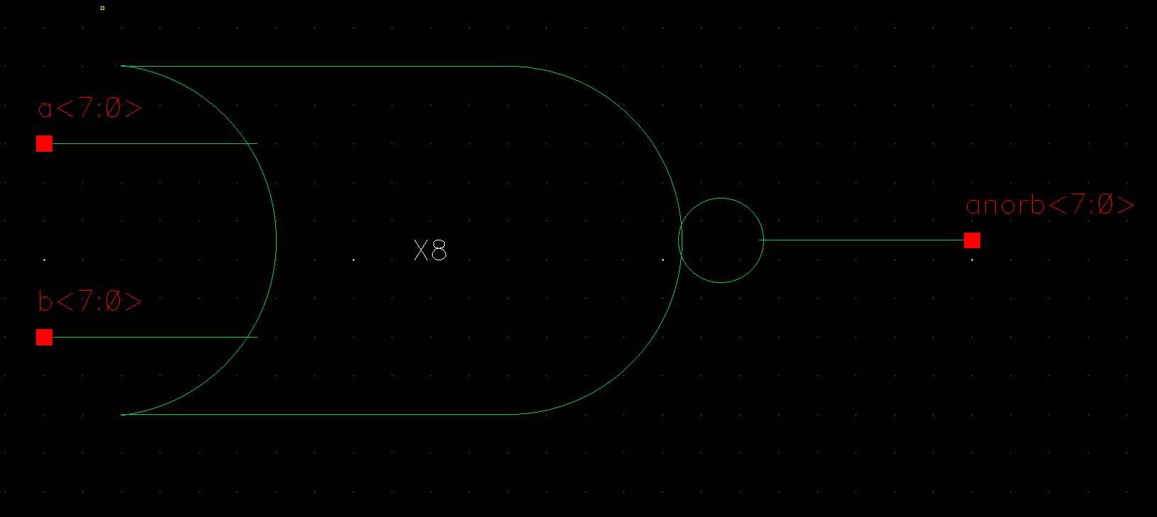
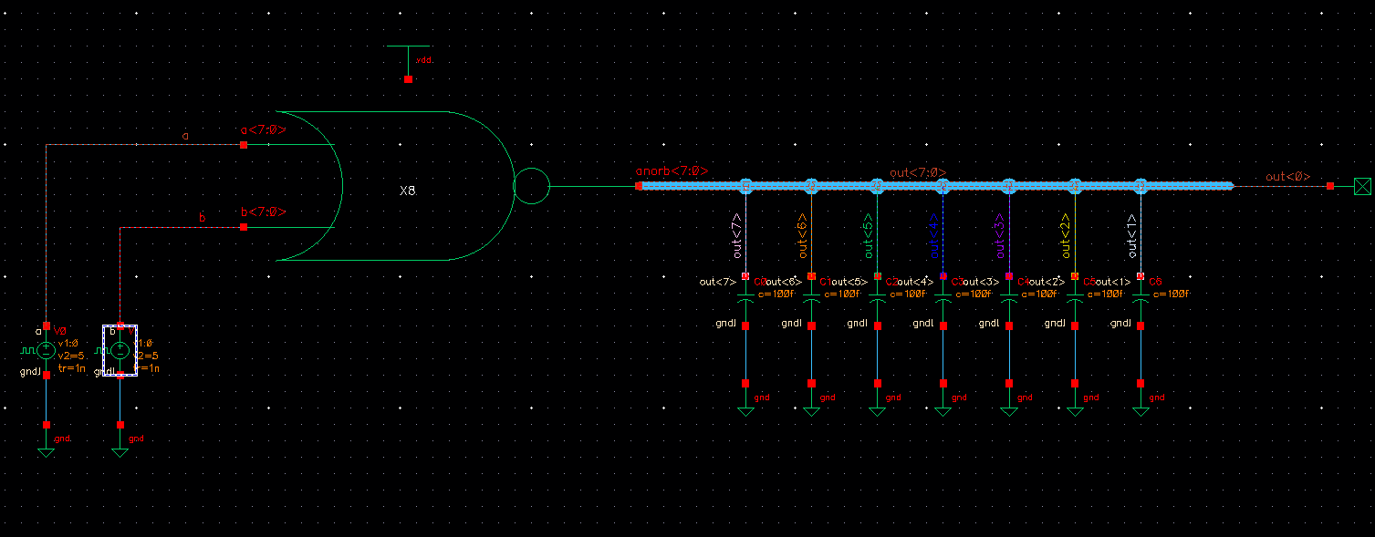
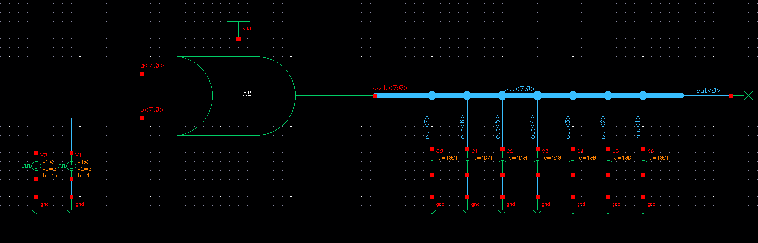
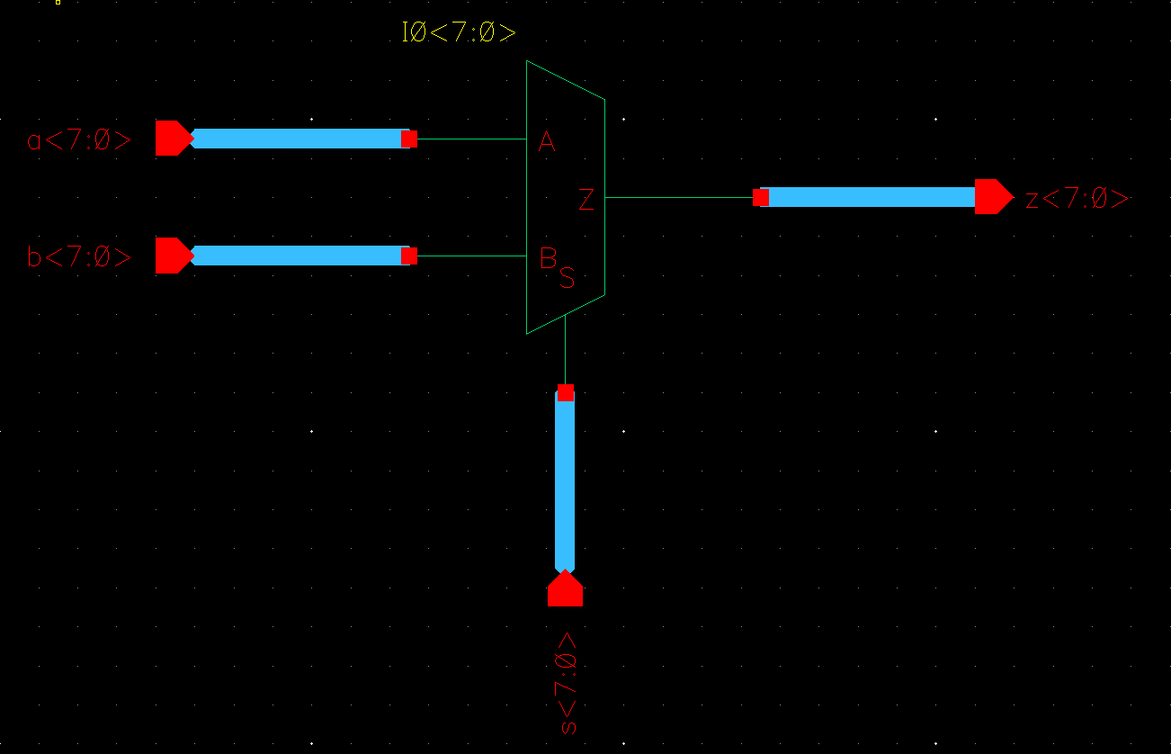
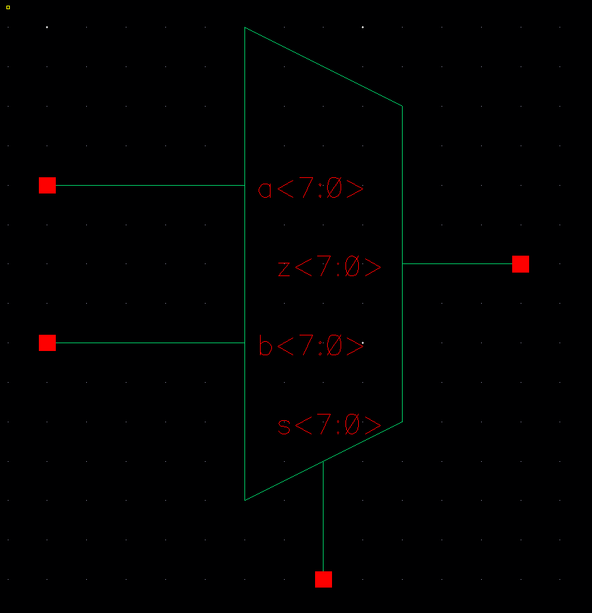
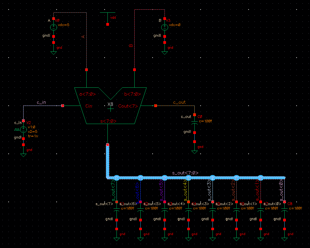
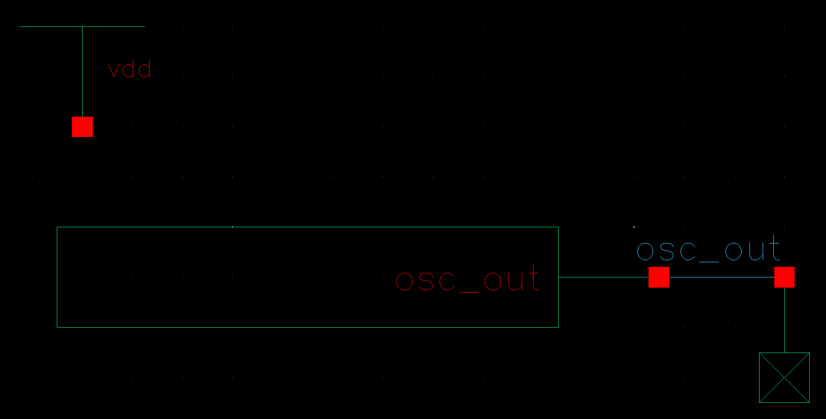
Next the tutorial explains a more concise and neater way of creating the same schematic but this time with the use of arrays and buses we're able to perform the same function but only using 1 symbol view of an inverter. This is done by editing the symbol values to tell cadence that we're actually using 31 inverters. This was done by putting an array next to the instance name(I0 <30:0>). After editing the symbol value I next had to use buses since we now how 31 instances of the inverter thus we needed 31 different inputs and outputs. However since the final output feeds back into the first input we had to make cadence aware of this. I did this by naming the final output a different name so that cadence knows the last stage of the oscillator ring feeds back into the first inverter.
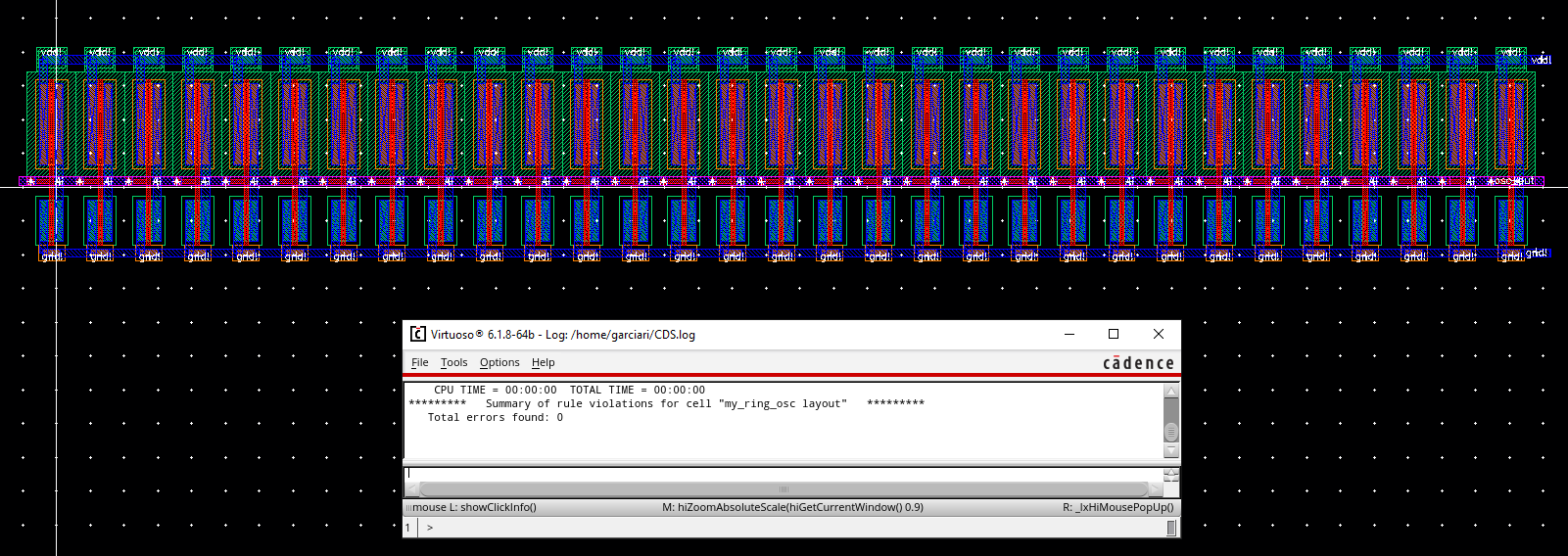
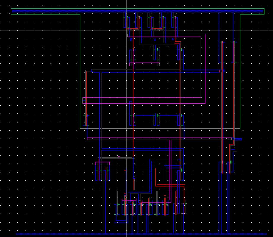
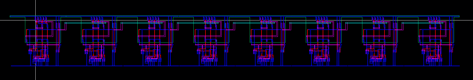
The next step is to layout the 31 ring oscillator. I was initially scared about performing this step since it means 31 different inverters however the tutorial showed me that I didn't have to layout 31 different inverters not even just 1 inverter. Instead I used my already created inverter from previous labs then added metal 1 extensions to extend my Ai(output of inverter), VDD and GND. After doing this I copied this inverter and inputted that I would be copying it 30 times. After laying out all 31 stages I next had to make a metal 2 connection from the 1st stage input to the 31st stage output to feedback stage 31 to stage 1. Thus I was able to layout the 31 stage ring oscillator in minutes.
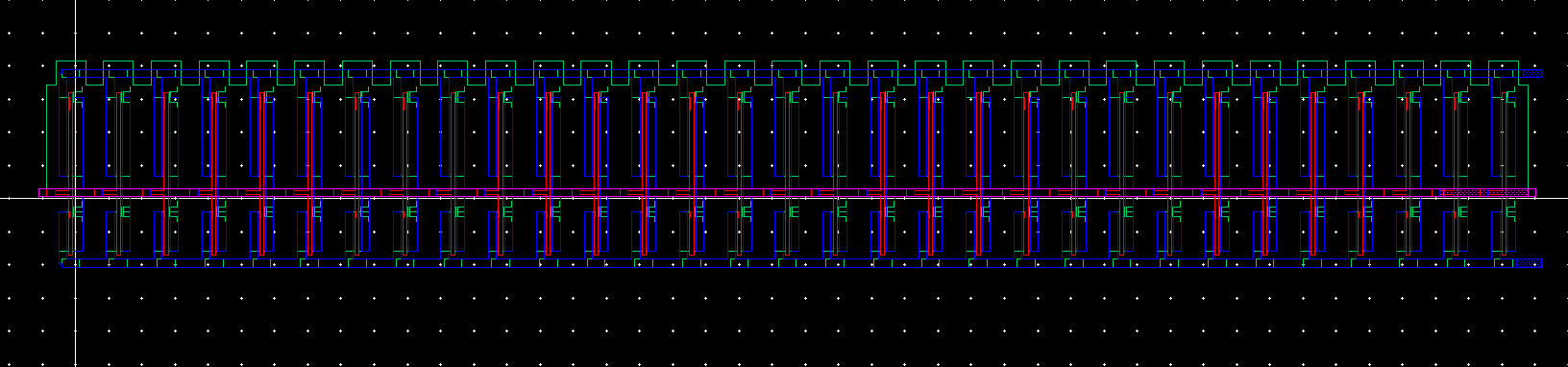
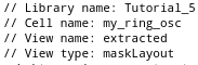
Extracted View
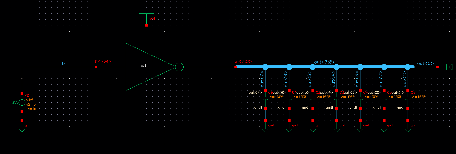
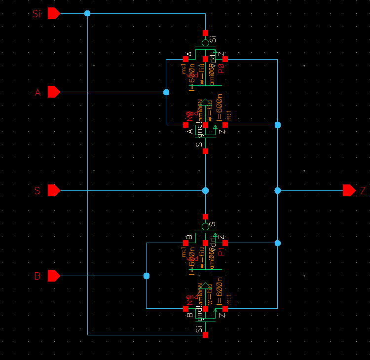
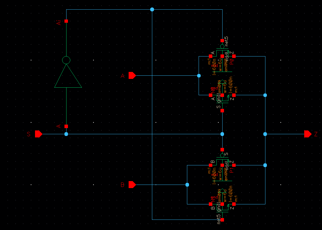
Edited schematic
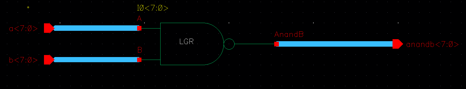
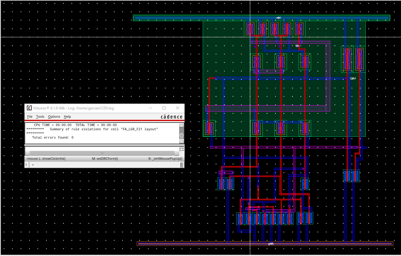
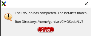
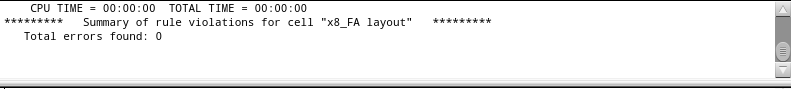
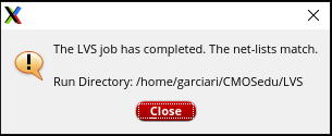
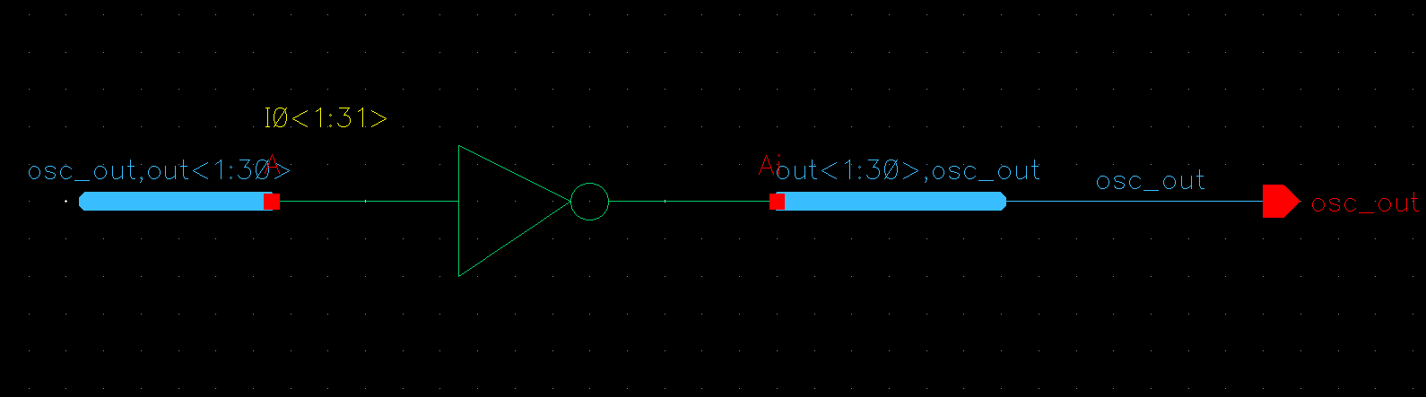
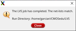
After laying out I next extracted my layout then ran an LVS which failed. It failed because the 31st stage set as an output in my layout but not in my schematic to fix this I edited my schematic by adding an output pin to the last stage so that we not only feedback the final output but also output it. With this modification I was now able to pass LVS.
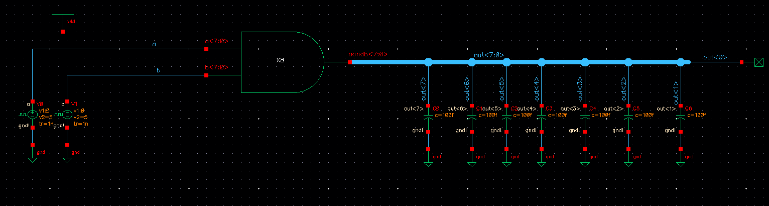
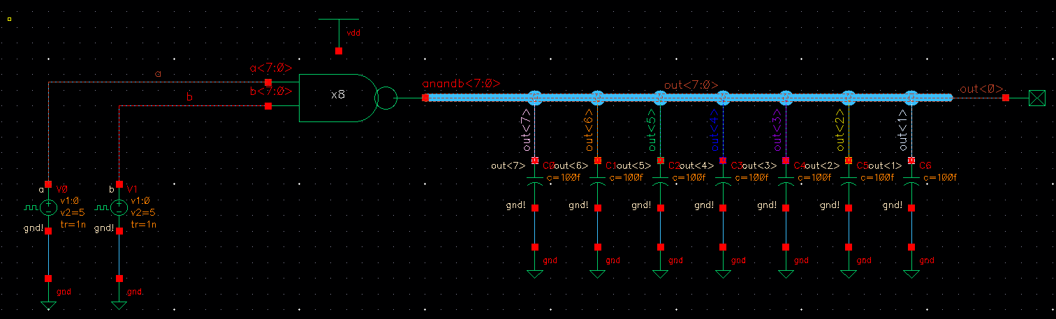
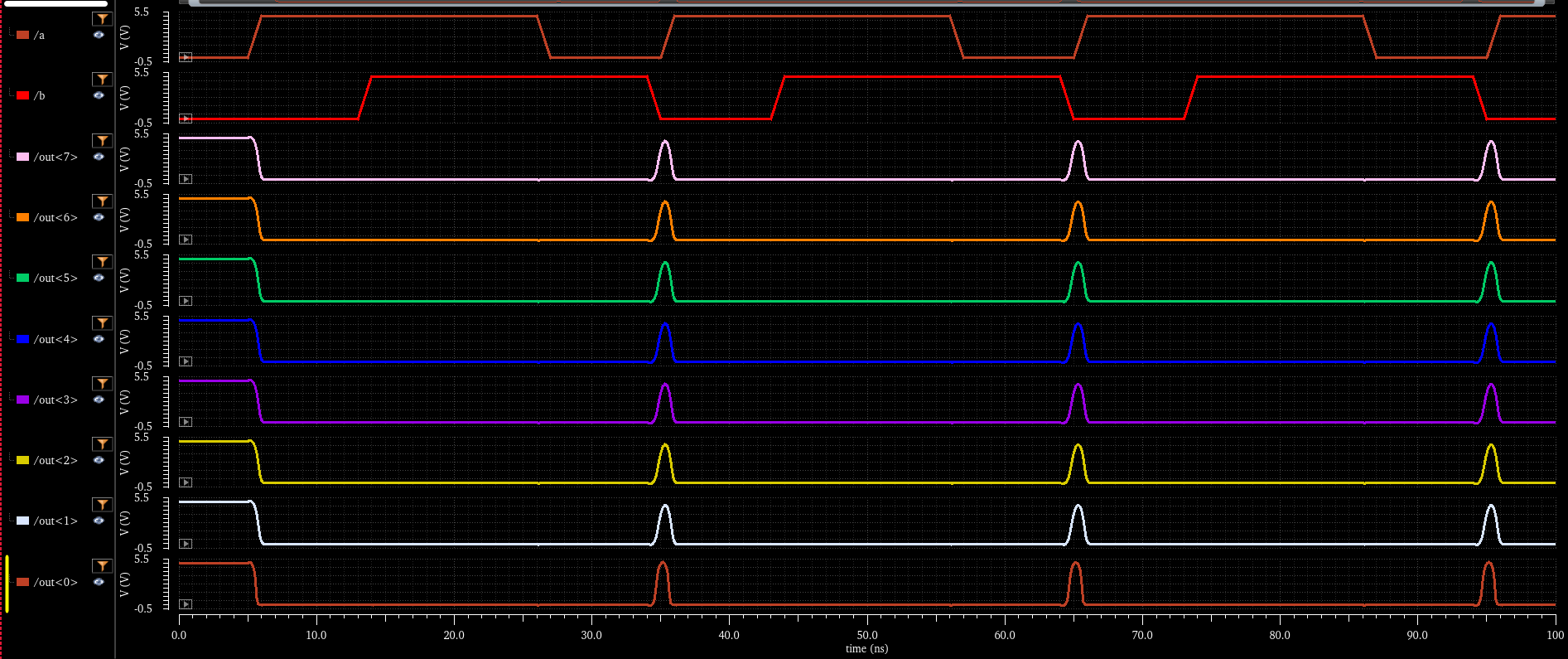
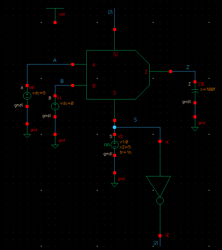
After passing LVS all that was left to do was simulate our schematic to make sure it works as intended by using the extracted netlist.
It simulates the same thus I succeeded. However to make sure it was infact using the extracted view for simulation I outputted the netlist and it shows that it was simulating using the extracted view.