Lab 6 Design, layout, and simulation of a CMOS NAND gate, XOR gate and Full-Adder - ECE 421L 

Authored by Luis Garcia Rivas,

garciari@unlv.nevada.edu

October 20, 2021


Prelab

1Schematic
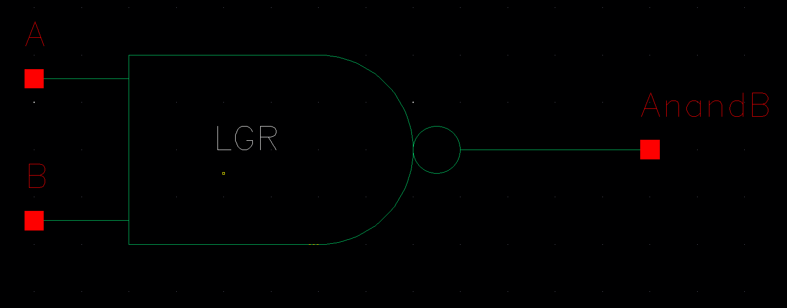
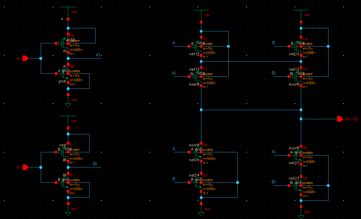
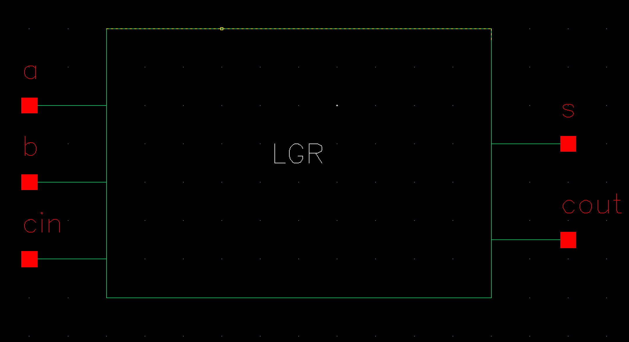
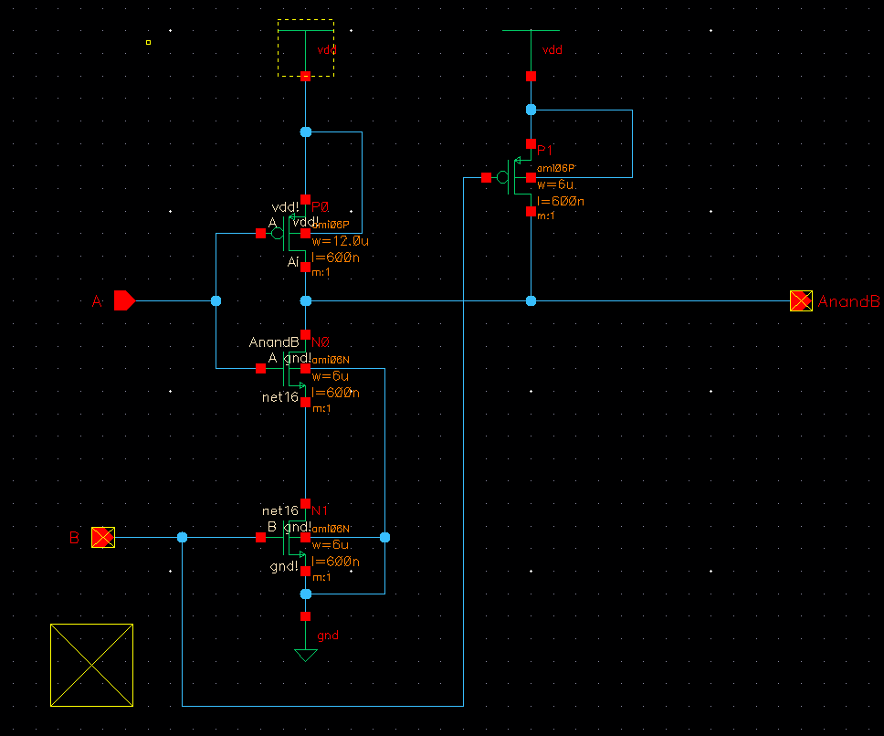
For the prelab,  I was tasked with going through tutorial 4 which shows the process for laying out a 2 input NAND gate. The first step for laying out a CMOS NAND gate is to first create a schematic with our input and output pins. In this case we only needed to add 2 inputs(a & b) and 1 output(AnandB). The schematic above has error markers because we're editing our previously created inverters so we haven't told the rest of our files that we are no longer creating an inverter. 
2Symbol
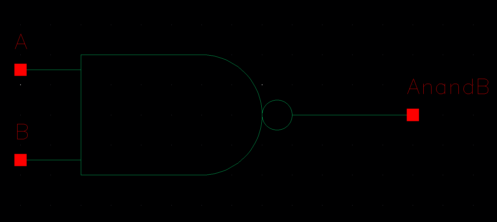
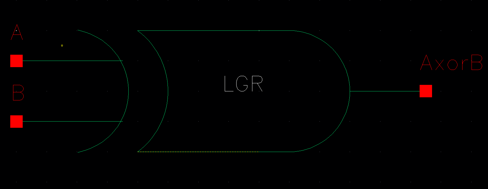
After creating my schematic I next created a symbol out of that schematic. This step is again really basic as I've done this multiple times throughout the lab. The only difference this time is I had to create a specific symbol instead of just a box. In this case, I had to create a NAND symbol.
3Layout
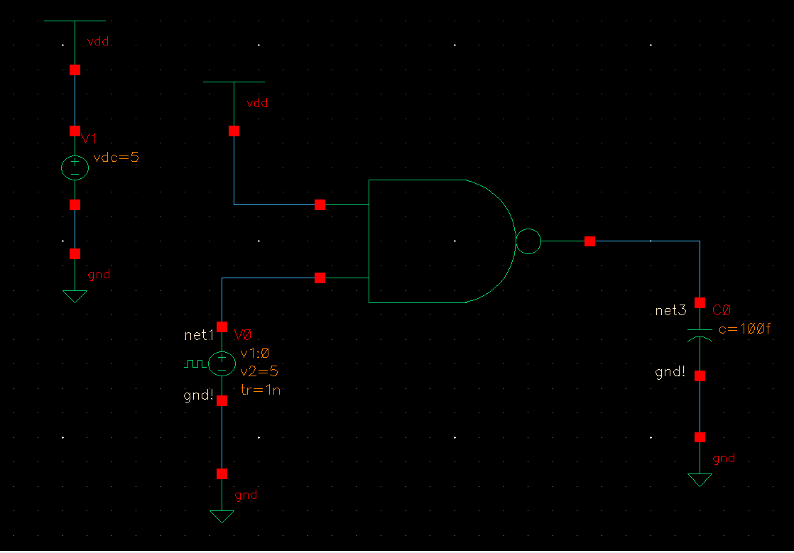
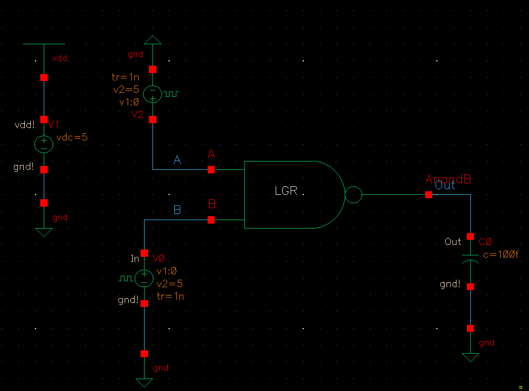
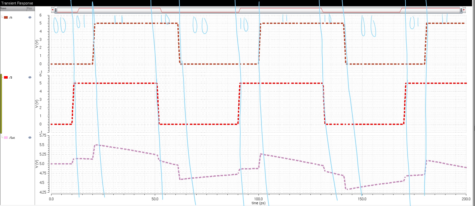
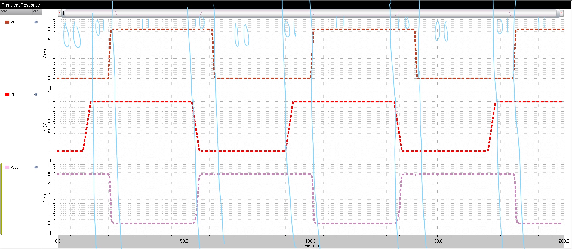
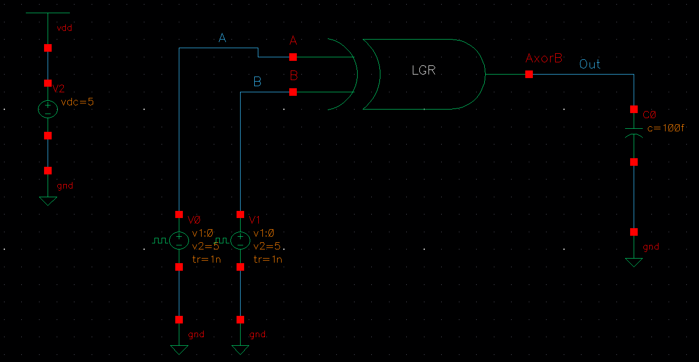
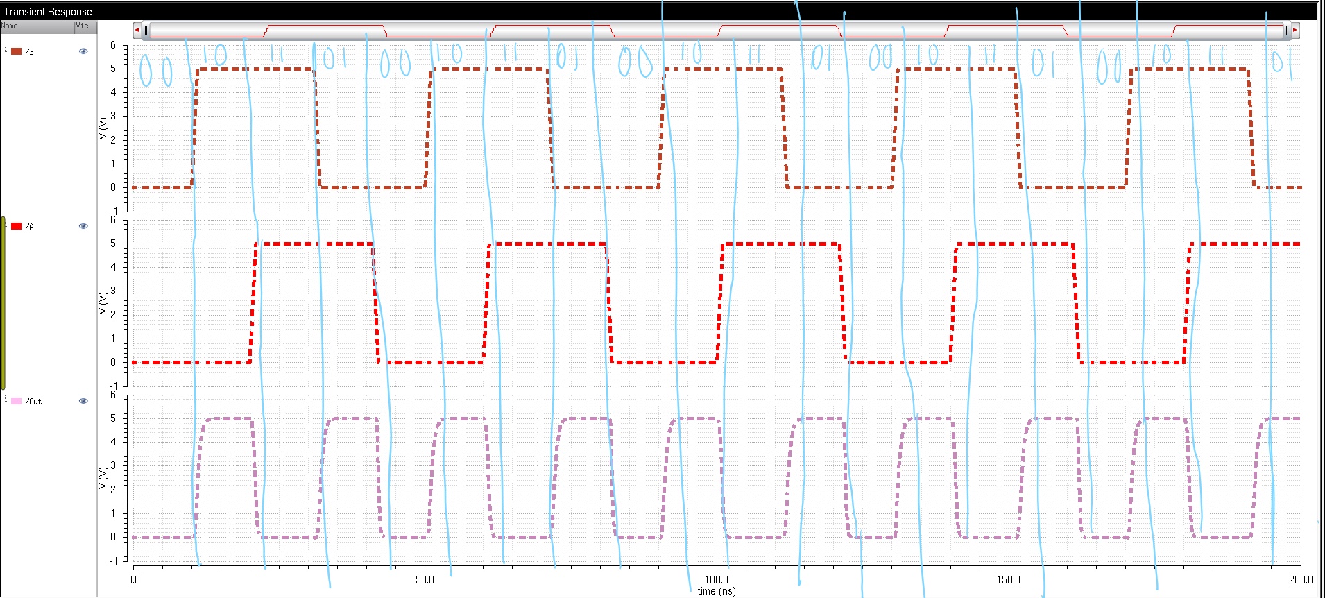
The next step was simmming the symbol to make sure that our schematic is correctly behaving like a nand gate.  To do this we added a pulse signal to one of our inputs so that it alternates between "0" and "1" (not exactly a digital since pulse signal is analog but you get the point.) and our other signal is set to VDD so it's always high.
SimResults
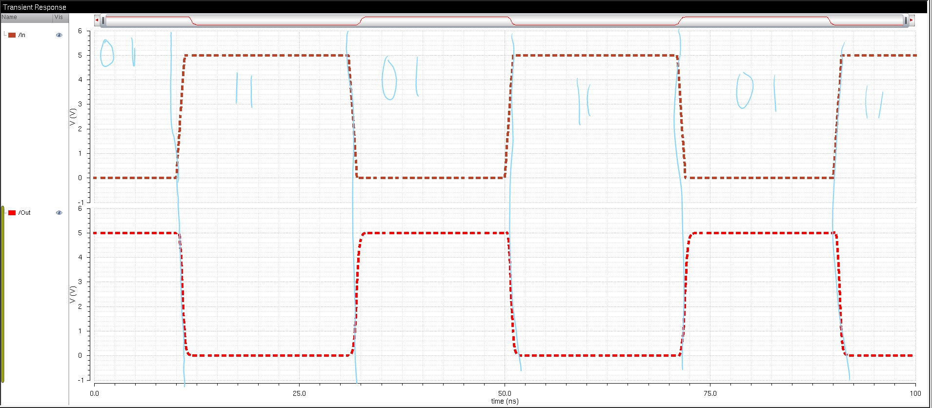
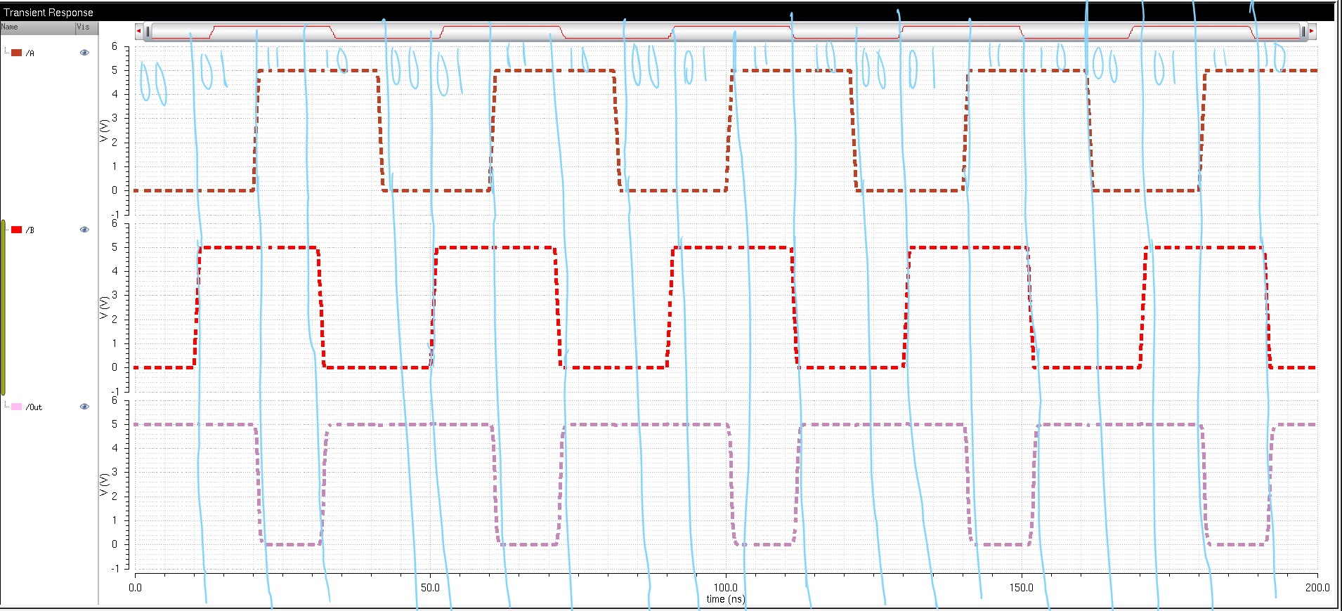
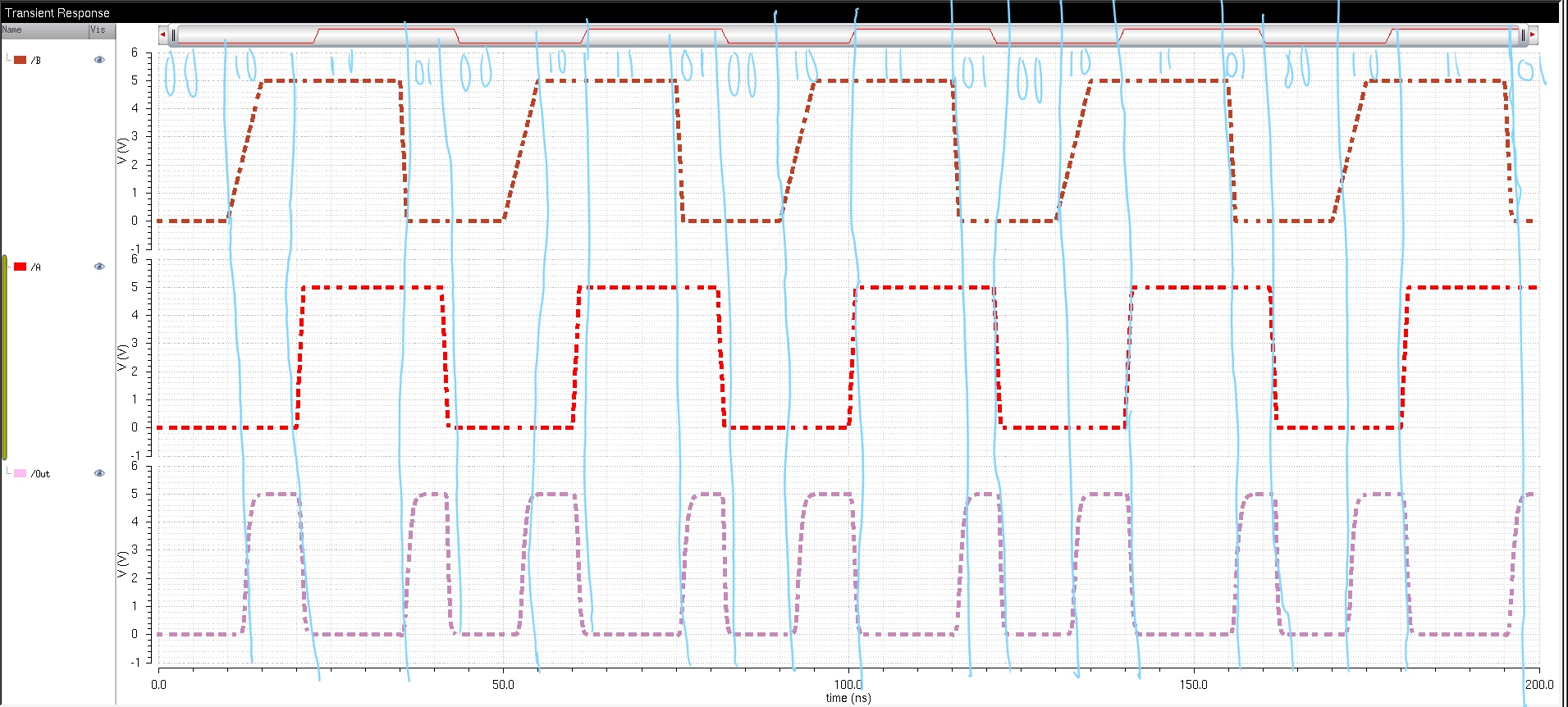
Following tutorial 4, we're only simming 2 cases. The first case both inputs are set to 1 in which case our NAND should output 0 and the case in which 1 input is set to 1 and the other is 0 which should output 1. As we can see in the screenshot above our schematic is in fact behaving like a NAND.
4Layout
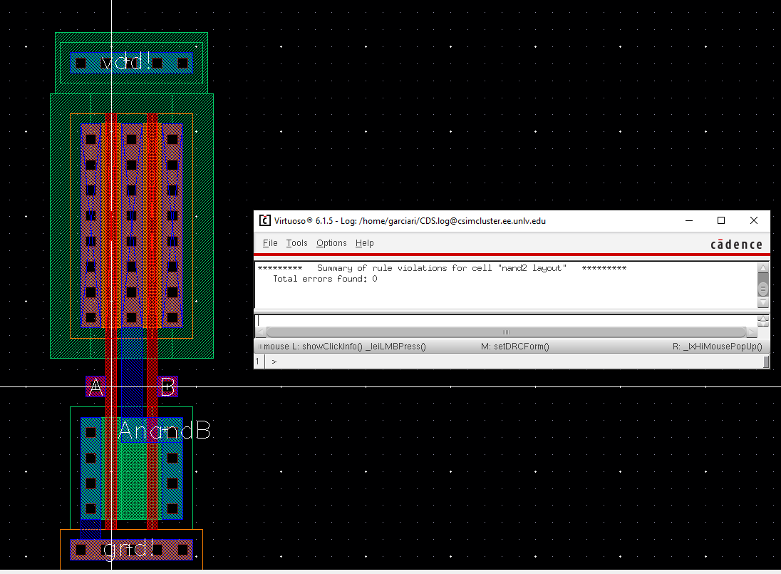
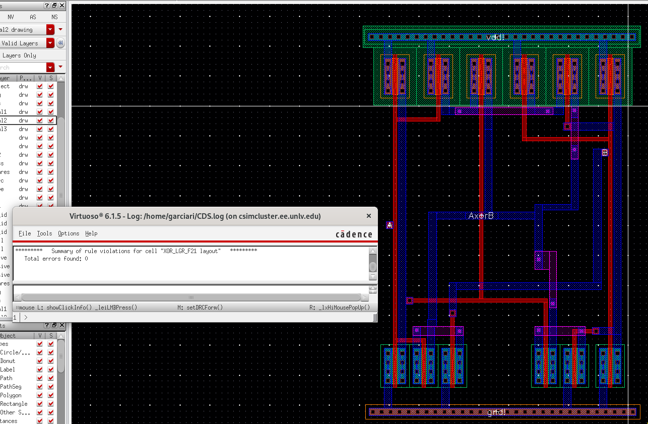
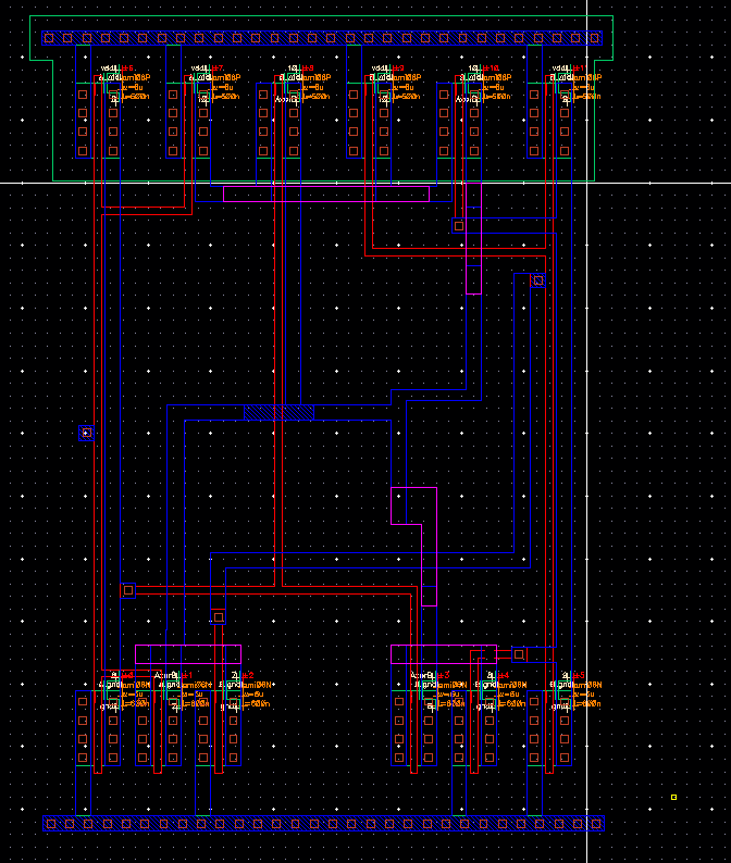
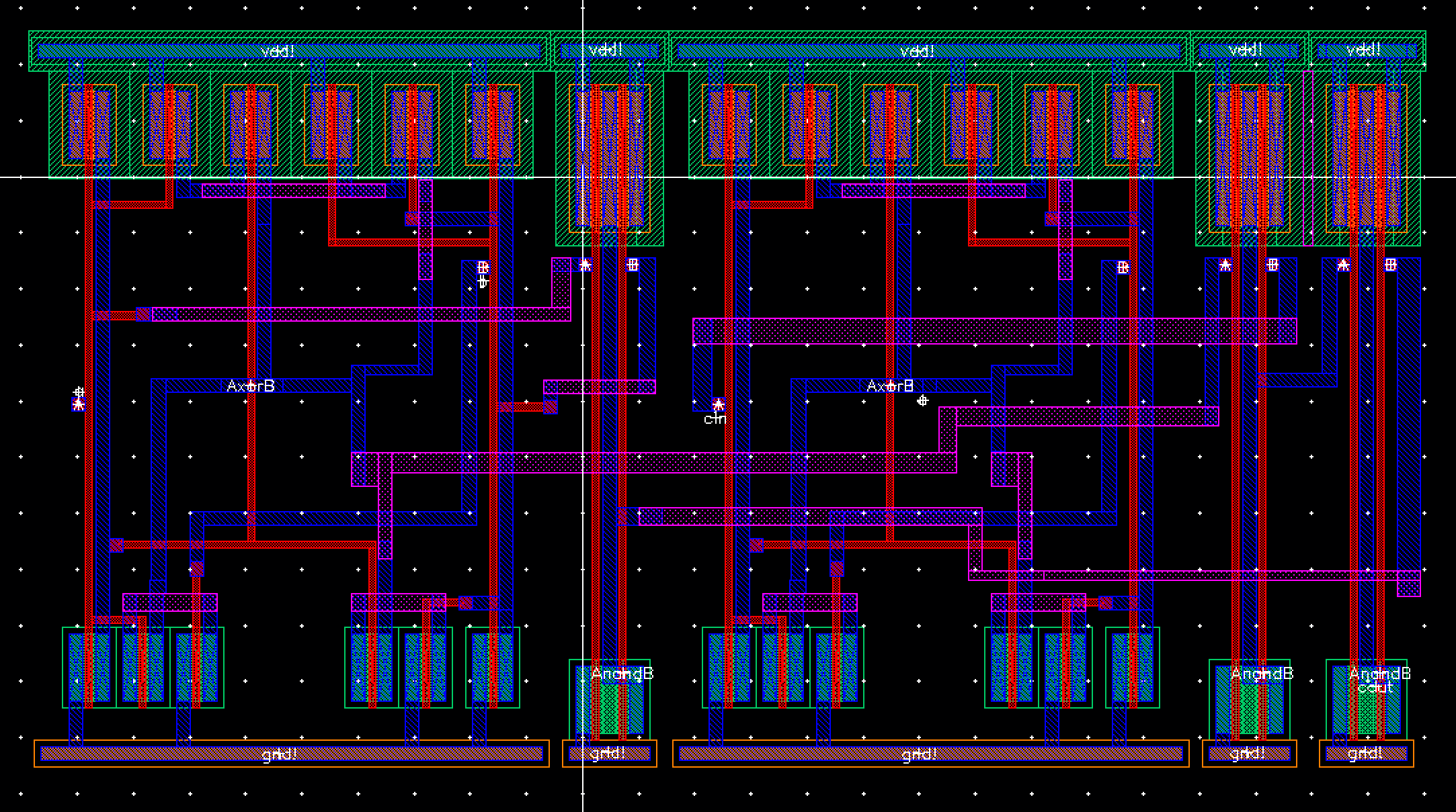
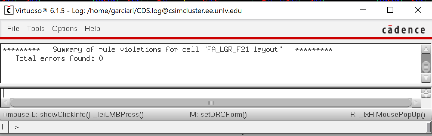
Since I've confirmed that our NAND schematic is in fact following NAND behavior I can move onto the next step in the tutorial which is laying out the NAND gate. This step was simple except that I've learned 2 new ways of laying out. The first is since our schematic has the drains of the pmos connected together, we can over lay the drains on top of each other in our layout to reduce width. The second is since both sources of our NMOS are connected together we can overlay 2 of the NMOS and remove the one of their contact areas to have a shared drain and source. I drc'd my layout to confirm my layout follows DRC rules and moved onto the next step.
5Extracted
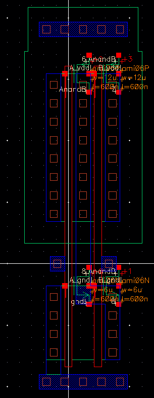
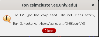
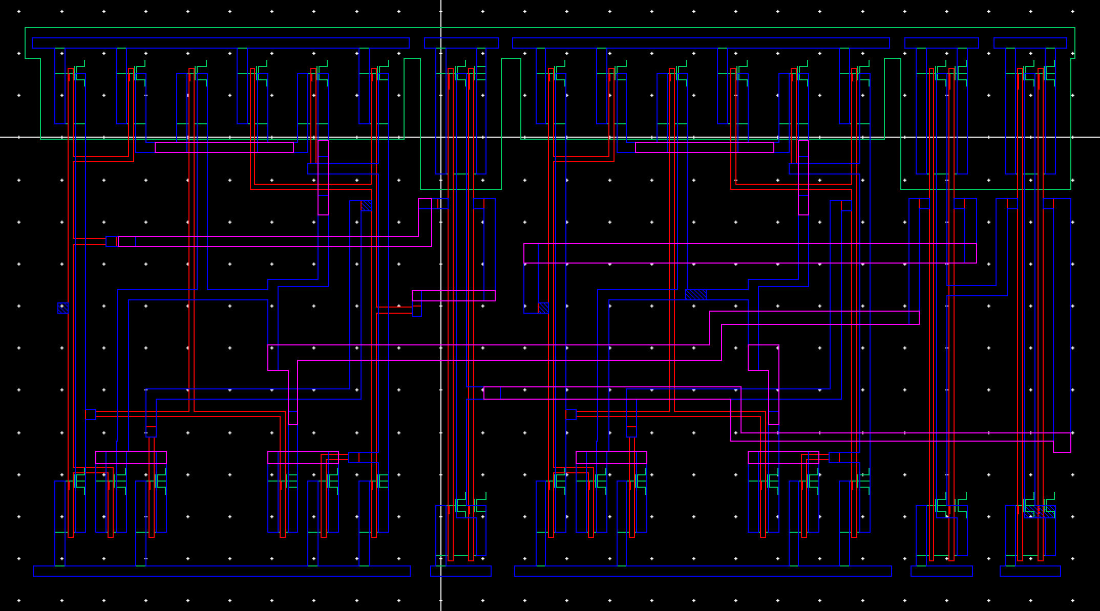
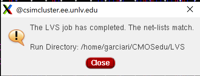
I next extracted my design and LVS'd to confirm that my layout fits LVS rules.
LVS
We passed LVS.
6LVS Output
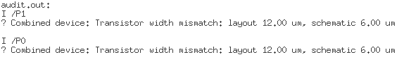
Normally we would be finished however we had an added step in which we see how our layout PMOS doesn't actually match the size of our schematic PMOS. To see this we had to edit LVS rules so that it would account for tracking FET sizing.

 Lab

2 Input NAND GATE

1schematic
For the first part of the lab we have to once again create a 2 input NAND gate. To do this I followed the tutorial since its the same gate. I start with creating a schematic of a 2 input NAND gate and since I'm using the inverter again I have an error since the rest of my files still assume inverter.
2Symbol
After creating my schematic I next created the symbol and like the prelab it must be an actual NAND symbol. The only difference is this time I was asked to put my initals in the symbol.
3Layout
I next moved onto laying out my schematic which again follows the tutorial since both the tutorial and the lab asked for 2 input NAND gate so difference shouldn't exist. After laying out we DRC'd the layout and passed so onto the next step.
4Extracted
I next moved onto extracting my layout and running an LVS to confirm that our layout is correct.
5Sim Schematic
I next moved onto simulating my NAND gate to confirm that our schematic follows NAND behavior as well as to see if timing glitches exist.
Sim Results
Per results above my nand matches nand behvior. 11 output 0 and 00 01 & 10 output 1.
Pico Sim
Simulation using PICO instead of NANO seconds
Mismatched Rise and Fall
SImulation with mismatched Rise and Fall Times

I next ran my simulations with different timings such as ps instead of ns, and mismatched rise and fall times. For the ps case our output was sketchy but that is due to the capacitor not discharging fast enough so our output is never fully 0. When simming with mismatched rise and fall times I don't see any major glitches but our output shows that we're dealing with an analog system since it doesn't instantly go change due to the delayed rise and fall times.

2 Input XOR Gate

1Schematic
I was next tasked with creating a 2 input XOR gate. This was slightly more difficult than the NAND gate since it is more complicated with the inclusion of 6 transistors.
2Symbol
After creating my schematic I next moved onto to creating a symbol. Again like the NAND, we have to create a symbol that matches the actual XOR symbol. After creating  the symbol I added my initials to the symbol and moved onto the next step.
3Layout
I next created my layout. This step was very difficult since I had to make sure that none of my lines were overlapping causing shorts. It was also difficult due to the amount of stuff going on so it was pretty easy to get lose track of what connects to what. To combat this I wrote down a guide to be able to reference throughout my time laying out. After finishing laying out I next drc'd to confirm my layout follows rules. We passed DRC.
4Extracted
I next extracted my layout and LVS'd my layout. We passed. I didn't use the FET size parameter option since I layed out my XOR gate without editing the PMOS and NMOS gates like I did with the NAND gate so the sizing would not change.
LVS
5SimSchematic
Sim Results
I next simmed my xor gate. The first sim was just to make sure that our XOR gate follows XOR behovior. 00 & 11 is 0 and 01 10 are 1. Our xor does in fact match the XOR behavior.
Pico Timing
Simulation with PICO instead of NANO seconds
Mismatched Rise and Fall Times
Simulation with mismatched rise and fall times
I next moved onto simming with different timing to find glitches and errors. As with the NAND case switching to ps instead of ns doesn't yield any meaningful results due to the sketchy output resulting from our capacitor not from our actual XOR schematic. With mismtached rise and fall times we don't get any major noticeable glitches but my simulation reinforce the fact that my system is analong since our output doesn't instantly change. 

Full Adder

1Schematic
For the final part of the lab, I was tasked with creating a schematic and layout of a Full adder. A full adder is a system in which 2 XOR and 3 NAND gates are used to create a system that adds in my case I add 2 1-bit numbers. I first start by creating a schematic of my Full Adder. A benefit of having already designed a XOR and NAND gate is that I don't have to create a schematic using transistors which would take long and be overly complicated.(36 transistors in total) Instead I just used my NAND and XOR symbols to create my schematic. My schematic has 3 inputs (a,b and cin) and 2 outputs(s, cout).
2Symbol
After creating my schematic I next created my Full Adder Symbol. 
3Layout
After creating my schematic I next moved onto laying out my full adder. To layout my full adder I used my previously created XOR and NAND layouts. Before placing them I had to plan out how to place them side by side to avoid shorting wires. After figuring out the best method I began to wire up the layouts. After this I DRC'd my layout to confrim that my layout does in fact follow the rules.
DRC Output
4Extracted
As with all other labs, after laying out and verifying DRC I moved on to extracting my layout and testing LVS. My layout passed LVS.
LVS
5Sim Schematic
After passing LVS, all that was left to do was to simulate my FA to test that my FA in fact matches FA truth tables. To test my Full Adder I first created a simulation schematic using my symbol I previously created. To test each condition I set 3 pulse signals for each input with each signal independent of each other. I then delayed each signal from each other by 5ns. a would go HIGH first after 5ns then B after 10ns and finally C after 15ns. I had to edit these values because unfortunately I would miss out on cases 101(a high b low cin high) and 010(a low b high cin low). To fix this I ran another simulation where b has 5ns delay a has 15ns delay and cin has 10ns delay. After simulating twice I was able to verify all 8 input cases produced the correct 8 output cases.
Simulation 1
5ns delay a, 10ns delay b, and 15ns delay cin
Simulation 2
15ns delay a, 5ns delay b, and 10ns delay cin
Case in which a has 15ns delay, b has 5ns delay and cin has 10ns delay has weird glitch after the case 111 in which cout has a slight dip. I believe this glitch occurs do the capactior being fully charged for too long.

Return to EE 421L Labs