Lab 2 - EE 421L
10-bit DAC design
A DAC is a system that converts a digital signal or an analog signal. Conversely, an ADC converts an analog signal to a digital signal. A common application of converters would be microphones and headphones/earphones.
For this lab experiment, we wil make use of a R-2R DAC to recreate a binary weighted DAC, such that the analogue output voltage is the weighted sum of the individual inputs.
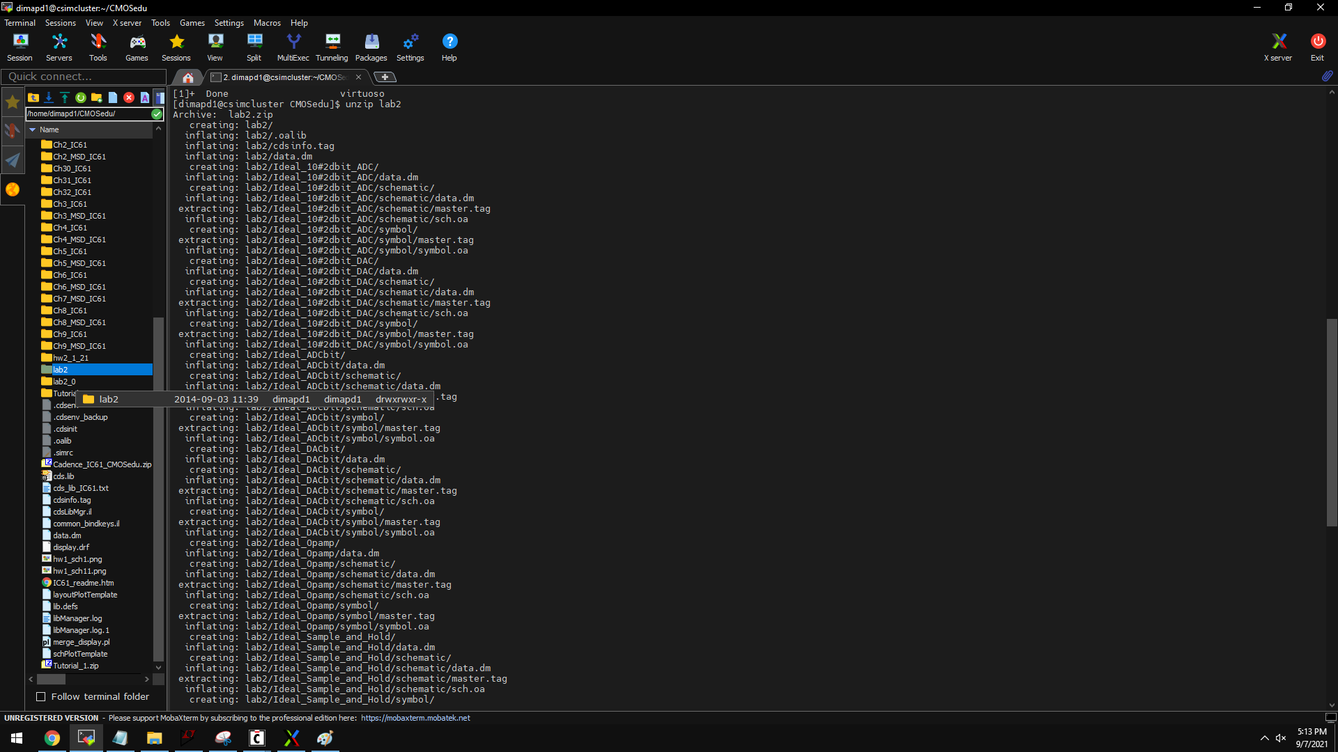
For the first part of the experiment, we will setup our working environment by downloading lab2.zip, uploading it to out csimcluster account under CMOS folder. Here we will extra the files we will be working with and go from there.
Simply use the unzip command to extract the folder, then make sure to define the location of the folder by adding
it your library.
Afterwards, we can now start with virtuoso. Lets first start by taking a look at the demo or example circuit provided.
In the image above, we see the ADC - DAC then our output. Our source would be a pulse signal which would be converted to a digital signal, then converted again to analog. We would not be altering the original input, therefore, we expect the Vin and Vout simulation to be overlapping to one another.
Because this is an example given to us, we can load the state of the session and use that as our reference.
In the simulation, we see that Vin and Vout are overlapping as expected. We didnt change anything, only transforming them from one form to another, therefore, we do not expect any losses. Note also, that we are using an ideal ADC - DAC for this example circuit.
Now that we have an idea on how the circuit works and supposed to behave. Lets start by making our own.
To start, lets make a copy of the ideal DAC. (image below, left side)
Then, lets open and edit the symbol of the ideal DAC, the schematic would show looking like the image above, right side. This will be out guide on how to make our connections. As per the lab instructions, we will be removing the VDD, Verfp, and Vrefm pins.
For the resistor, I made a copy of a previous example circuit, saving the copy under lab2 folder, and performing the edit from there.
From here, we can start to make our 2R - R resistor. Since the lab experiment calls for a 10k. We will set the values of all resistors to 10k ohms. For the 2R resistor, we will recreate this by putting 2 resistors in series.
Make sure to always save and check your circuit. The last thing we want at this point, is to lose our progress. Likewise, when making simulations, be sure to save the state, no matter how many different states. The more simulation states you have, the more it makes sense to create meaningful titles, instead of state1, 2, 3, etc.
After creating the 2R-R schematic, lets make a box/symbol.
We do this by Create/cellview/from cell view...
create
the symbol, choose where you want the pins to be. Here, you can start
to visualize how you want your blocks to connect to one another.
After doing so, lets make a new cell under lab 2. Here, insert the instance of the block symbols we created.
Again, save and check then create a block/symbol. Then lets make us of the symbol to start finalizing our DAC.
In the new cell, where we insert the instance/block/symbol we created (image above), lets test our circuit to make sure it behaves the way we expect it to be.
In our simulation, we can verify the time it takes for the capacitor to start charging, making use of the markers,
bindkey M and taking the difference, bindkey D.
This also proves the delay which is part of the questions to be answered in our lab report. At this point, we can start to replace the ideal DAC in the demo circuit with our DAC. Do the the testing to verify that we are getting the same input as output and same sine wave/simulation as the ideal DAC. We can further prove the accuracy of our design, by testing it with different loads and proving via hand calculations and cadence simulations.
Thank you for your time, cheers,