Lab 2 - EE421L
Damian Aceves Franco
acevesfr@unlv.nevada.edu
09/01/2021
Design of a 10-bit digital-to-analog converter (DAC)
Pre-lab work
- Read through this entire lab write-up before doing the pre-lab
- Download lab2.zip to your desktop.
- This
archive contains a simulation example using an ideal 10-bit
Analog-to-Digital Converter (ADC) and Digital-to-Analog Converter
(DAC).
- Prior to coming to lab make sure you understand how the input voltage, Vin, is related to B[9:0] and Vout.
- In your lab report:
- 1) provide narrative of the steps seen above,
- 2) provide, and discuss, simulation results different from the above to illustrate your understanding of the ADC and DAC,
- 3) explain how you determine the least significant bit (LSB, the minumum voltage change on the ADC's input to see a change in the digital code B[9:0]) of the converter. Use simulations to support your understanding.
up load lab2.zip to MobaxTerm and unzip
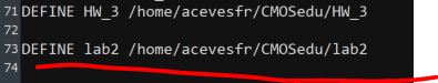
then check to see if the design directory is in the cds.lib if now type it and save
now run virtuoso and open the schematic
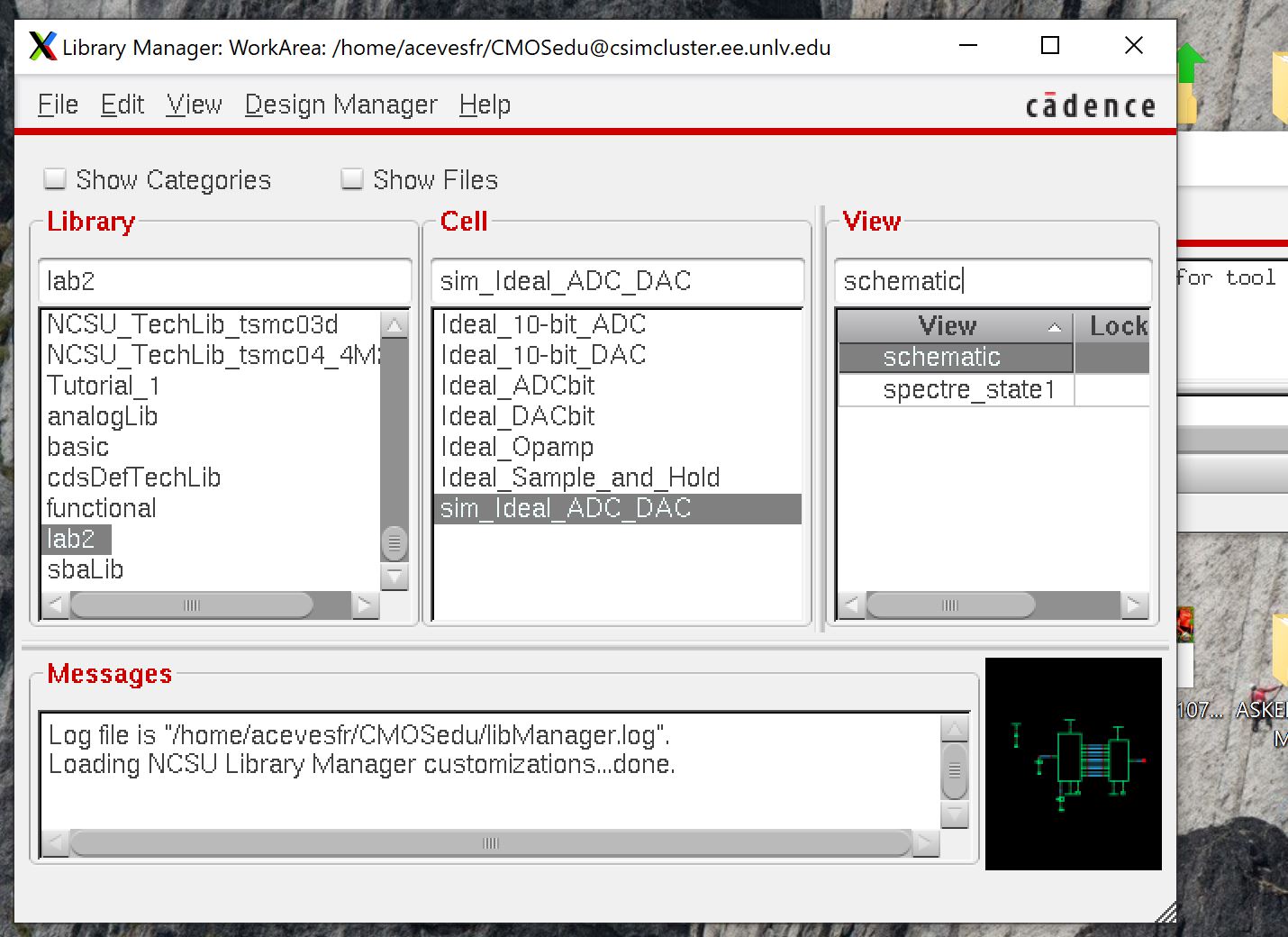
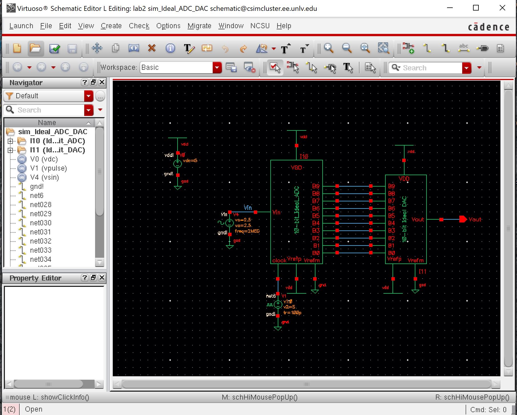
then run ADE L
The least significant bit (LSB) is determined my useing the equation 1LSB=(Vdd)/2^n.
in this case the 1LSB is 5/2^10 = 4.88mV
****************************************************************************************************************************************************************************
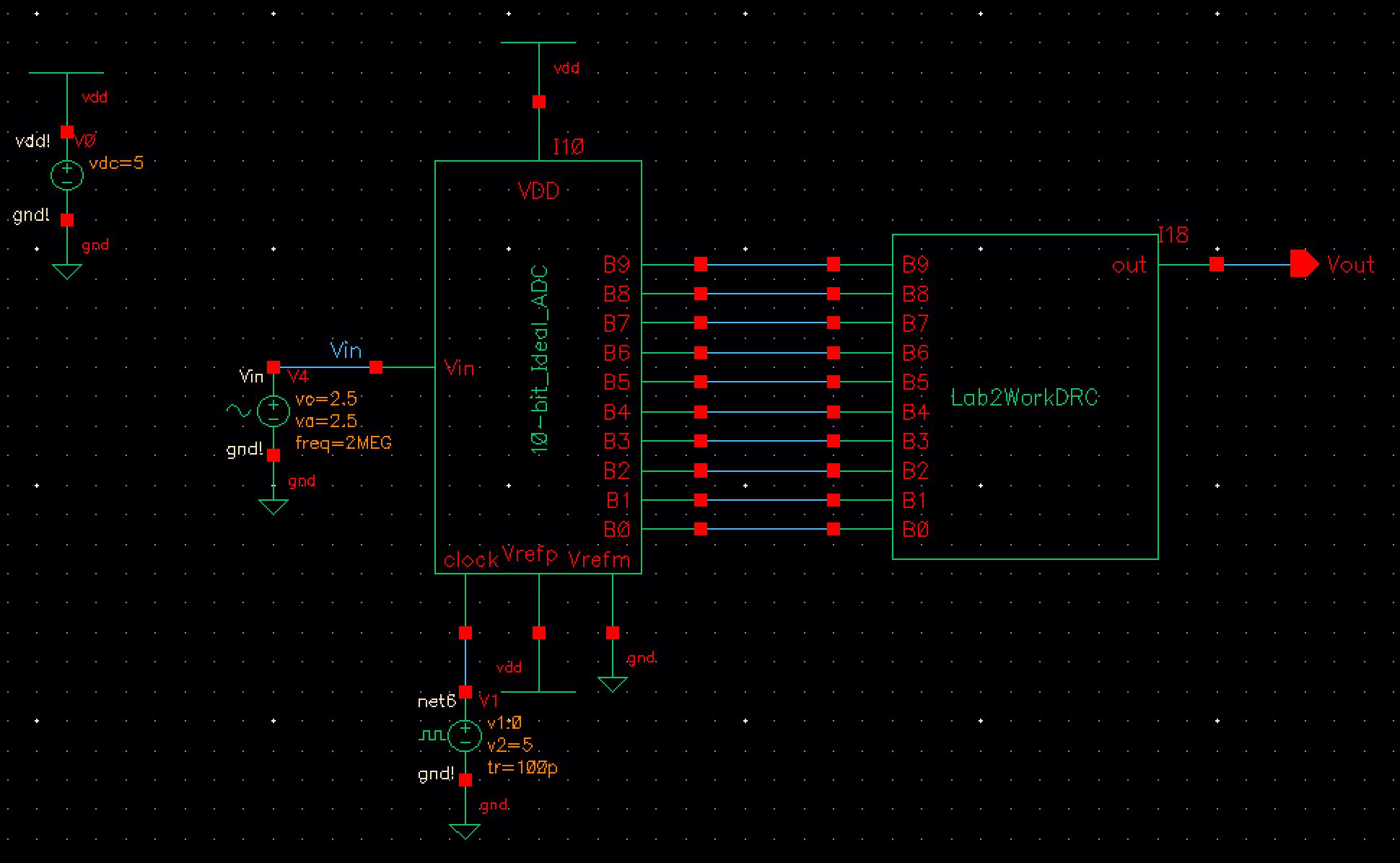
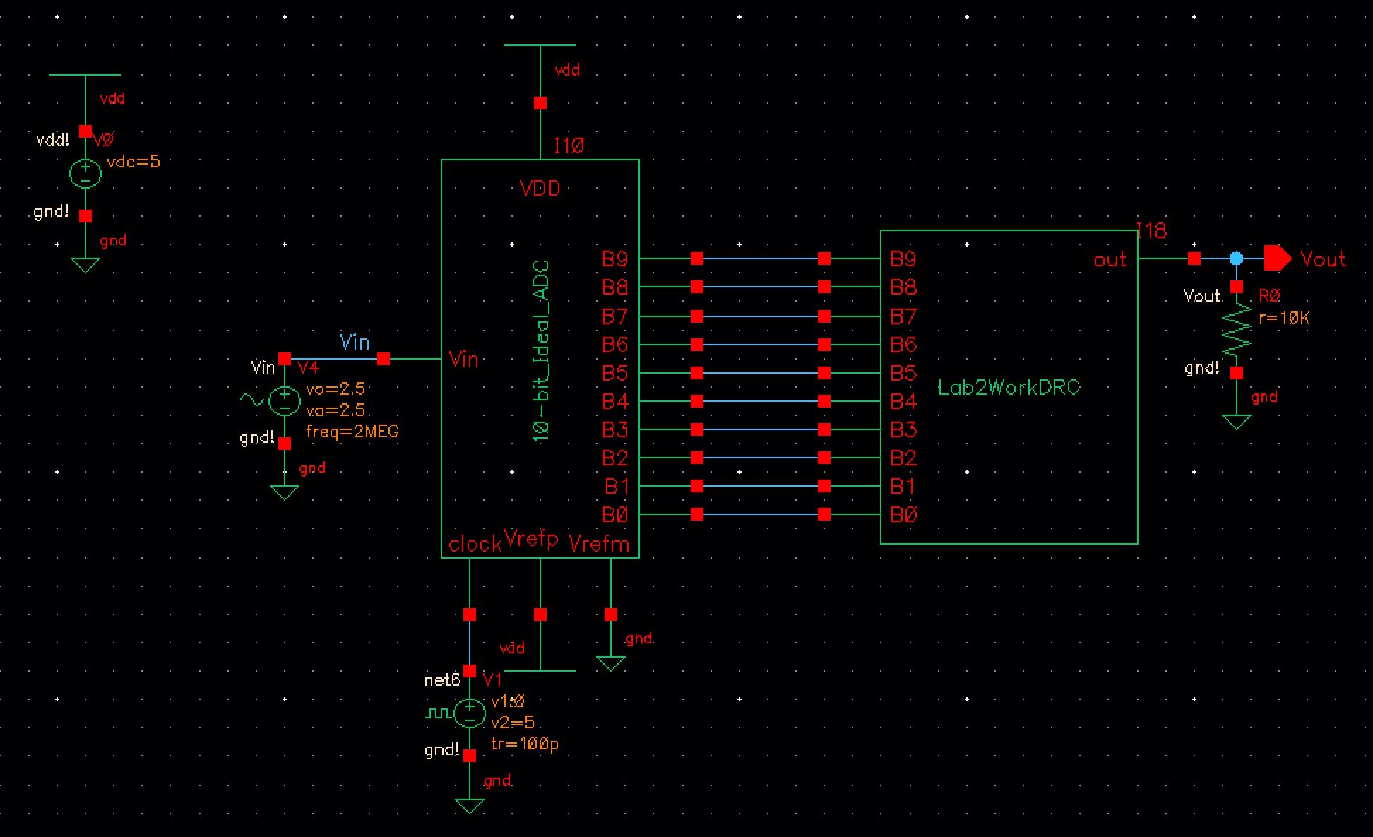
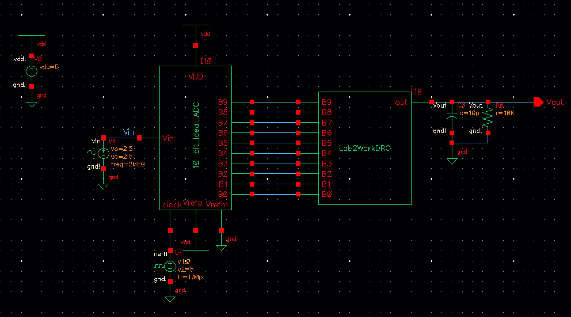
In this lab we'll use n-well resistors to implement a 10-bit DAC.
- The design of a 10-bit DAC using an n-well R of 10k
- How to determine the output resistance of the DAC (answer: R) by combining resistors in parallel and series
- Delay, driving a load
- How to create a symbol view for your design with the exact same footprint as the Ideal_10-bit_DAC symbol view
- Simulations to verify your design functions correctly
Our design is based upon the topology seen in Fig. 30.14, below, in the CMOS book.
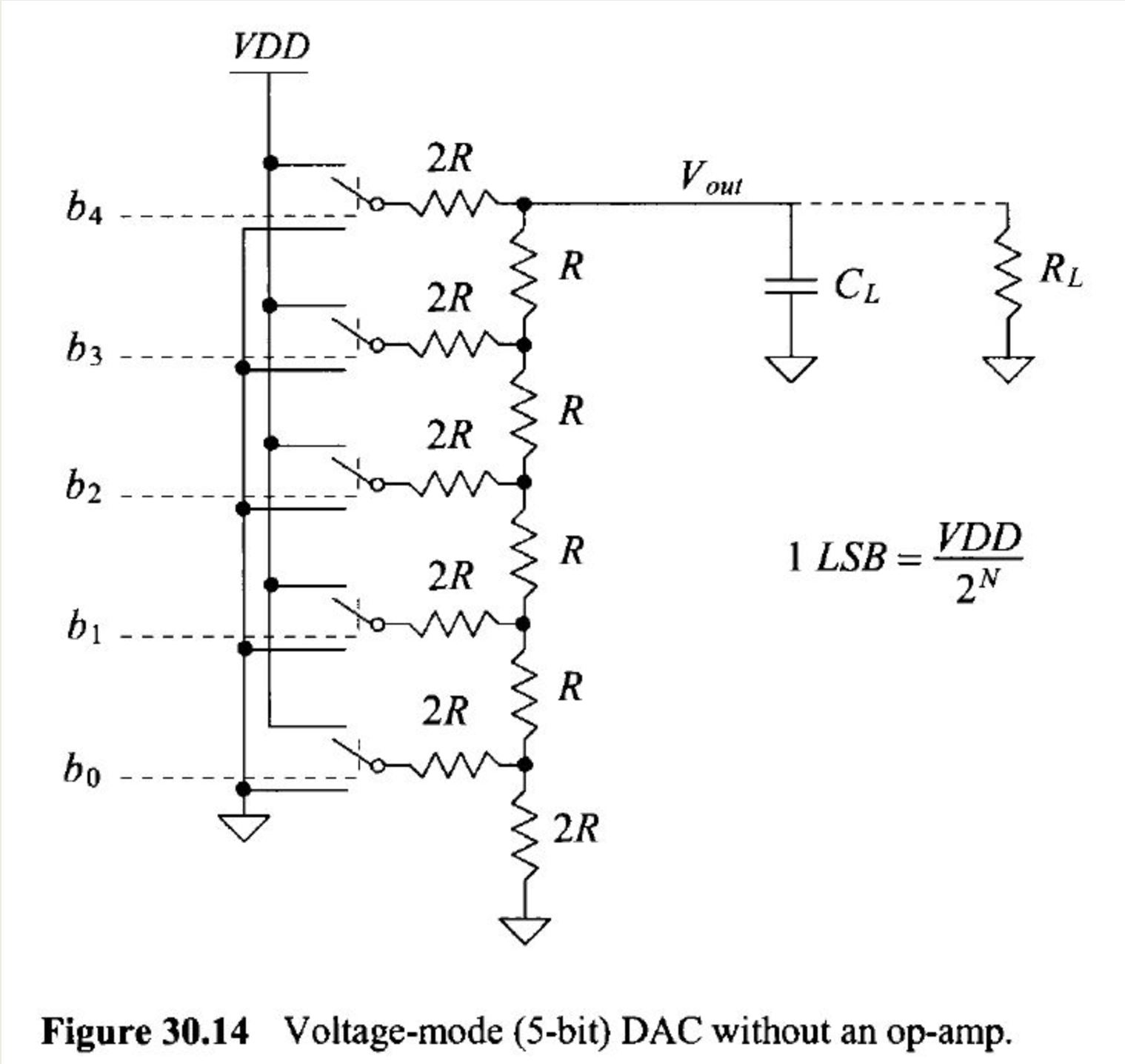
Desinging 10-Bit DAC using N-well Resistor of 10k
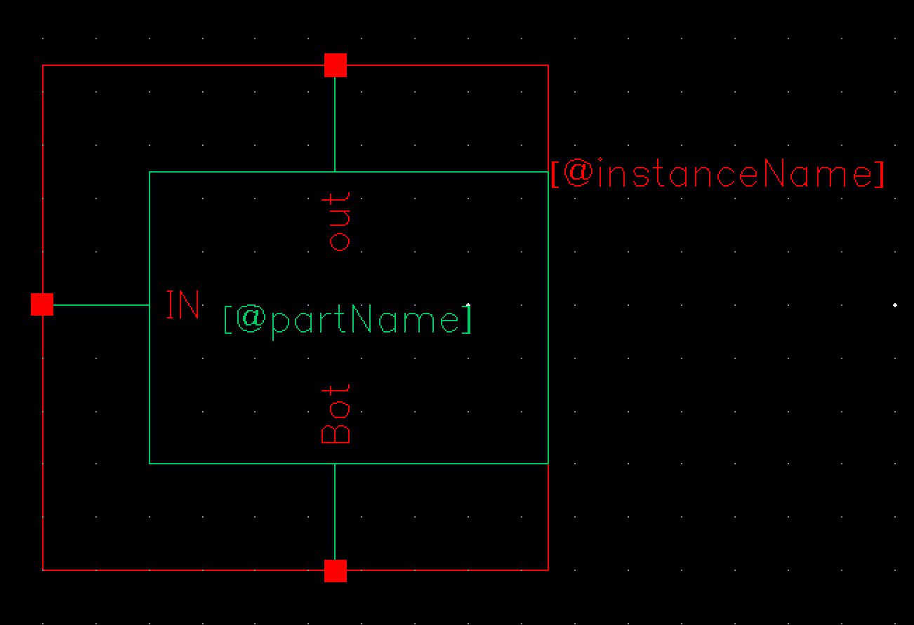
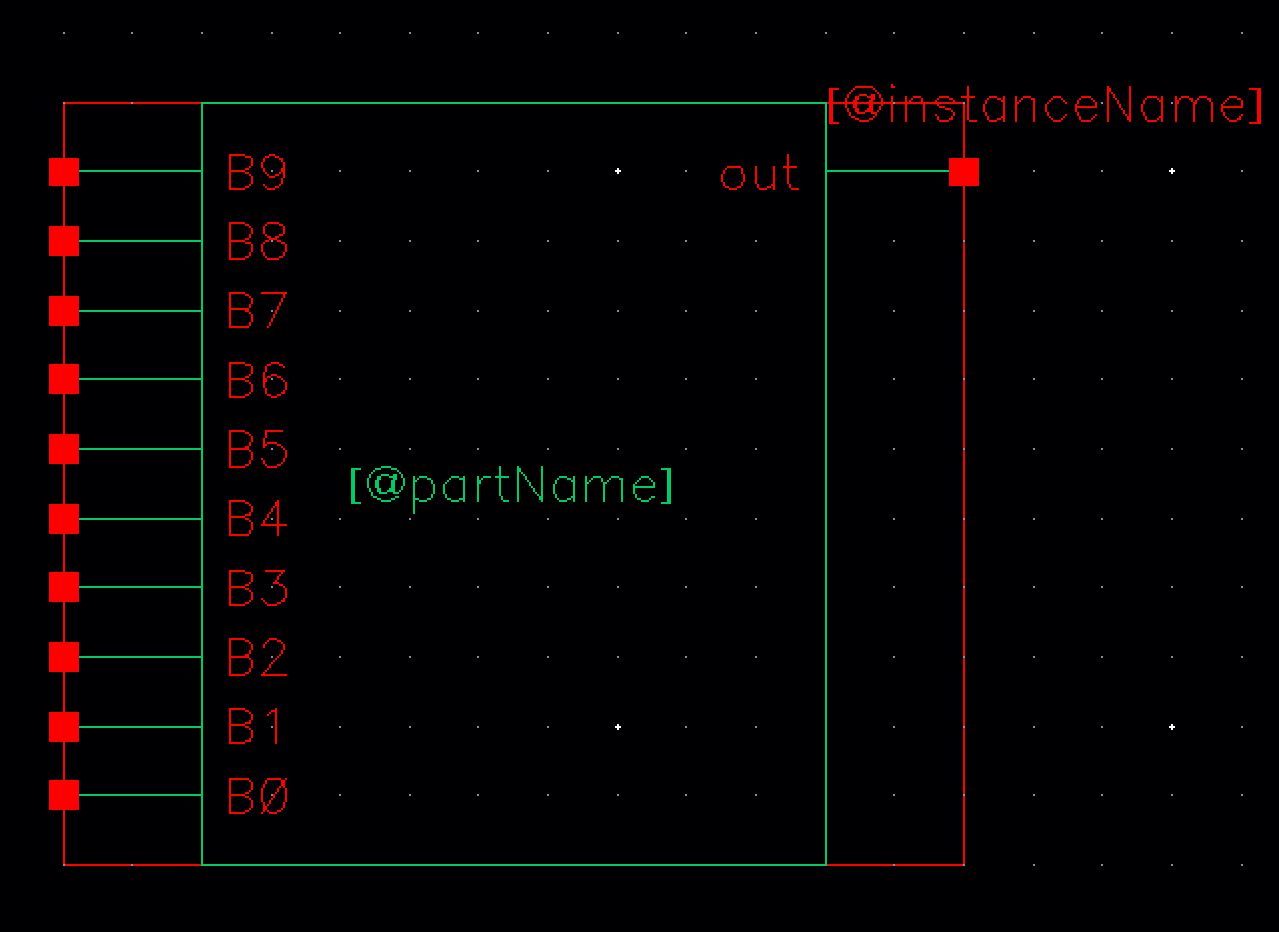
Create a symbol
We
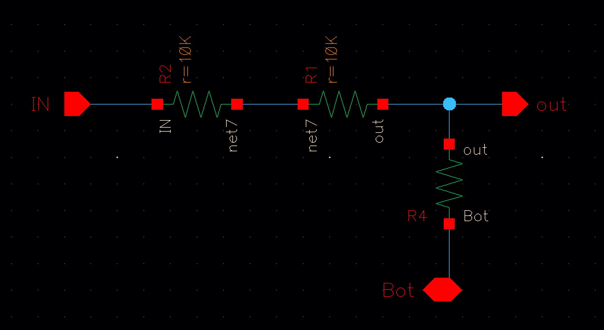
are ready to start the fun. Next I created a new schematic and lined up
the new symbol in the following manner to start making the DRC
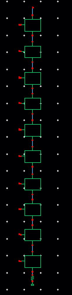
Now we must remember to add a 10K resisitor at the bottom in between the symbol and gound
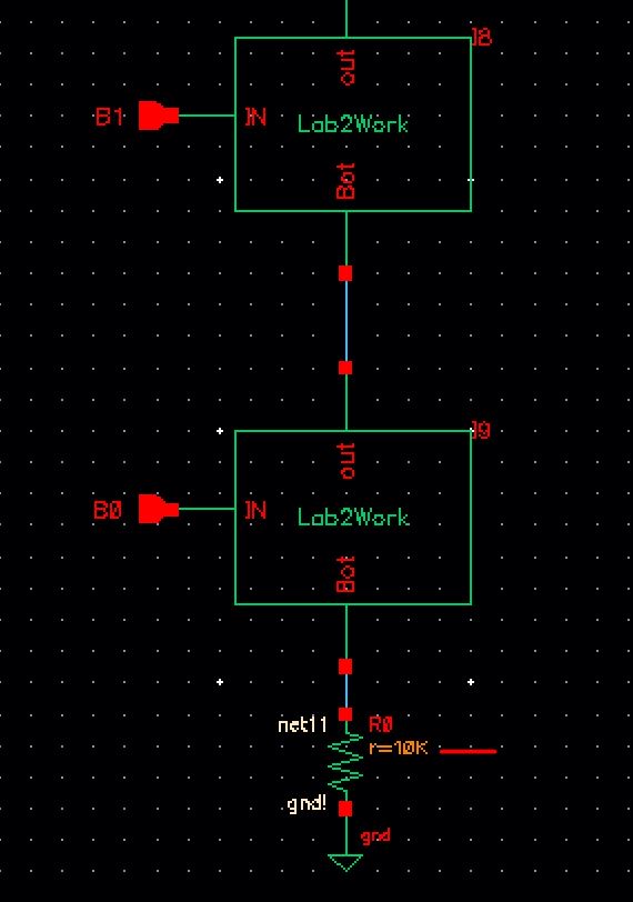
We then create a symbol again this time puting pins B0 to B9 on the left and out on the right
Now
that we have assembabled the DAC we are ready to begin testing
next, we are going to test by grounding all the inputs but B9 and
looking at the output delay at 50% of the input
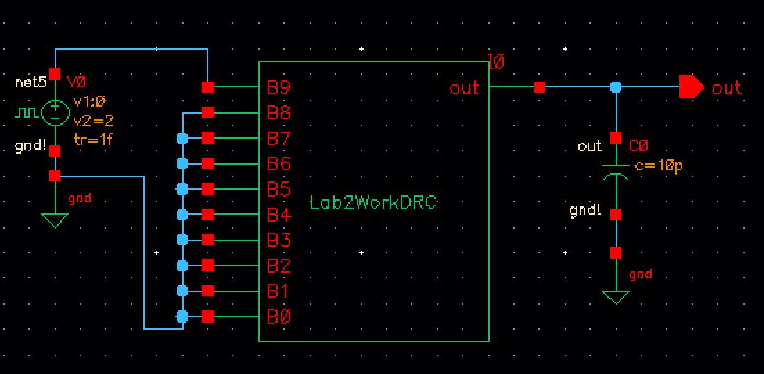
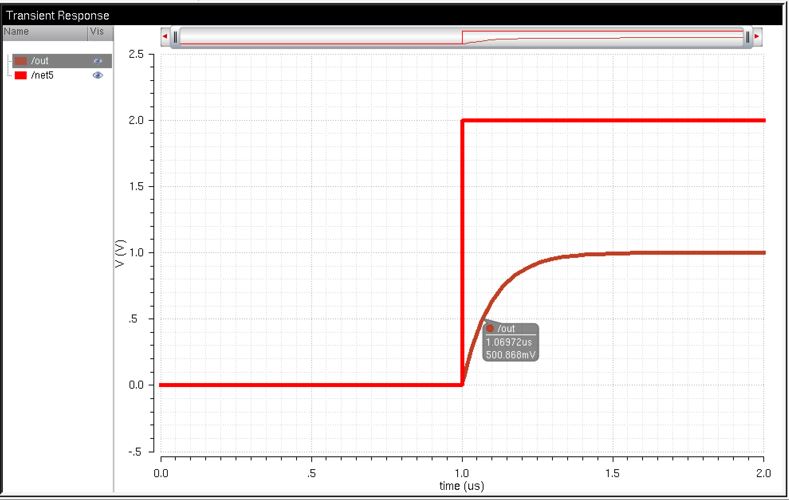
Now we compare the sim with the handcaluations we see that the they match. Yay!
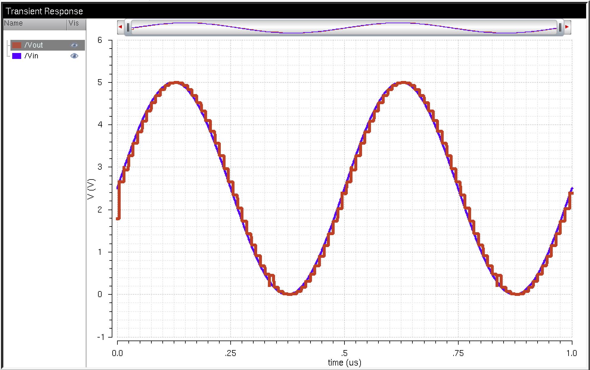
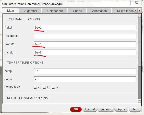
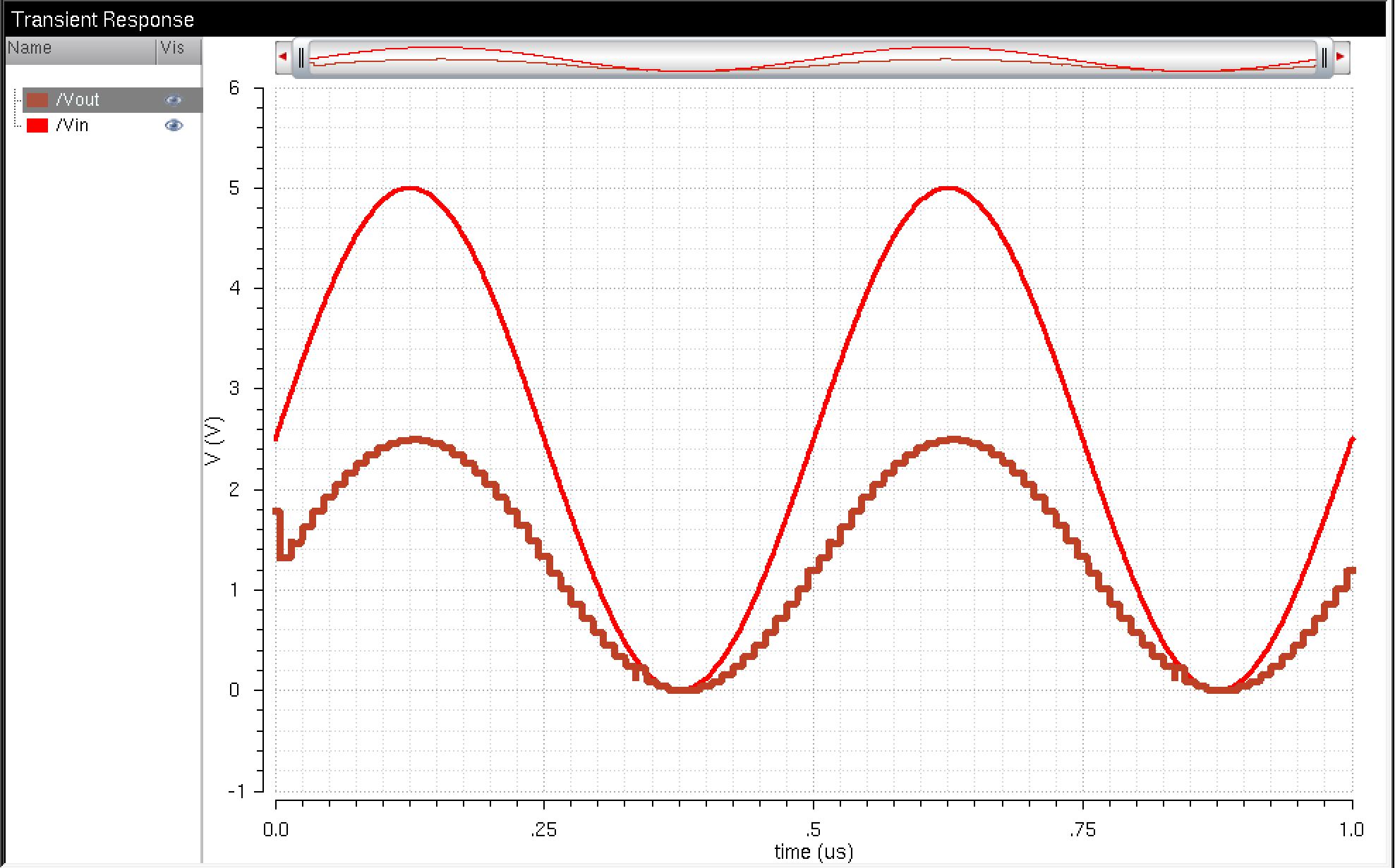
Next we continue testing the made DAC with no load by Putting the made DAC in the schematic of the prelab in play of that DAC. Before running the sim in ADE I had to for the simulation to converge by going to in the ADE, Simulation -> Options -> Analog. And set the following values. We can see the output matches the output from the ideal DAC form the Prelab!
Next tesing with a 10K resistive load, and we should get half of the input voltage. Yay we do!
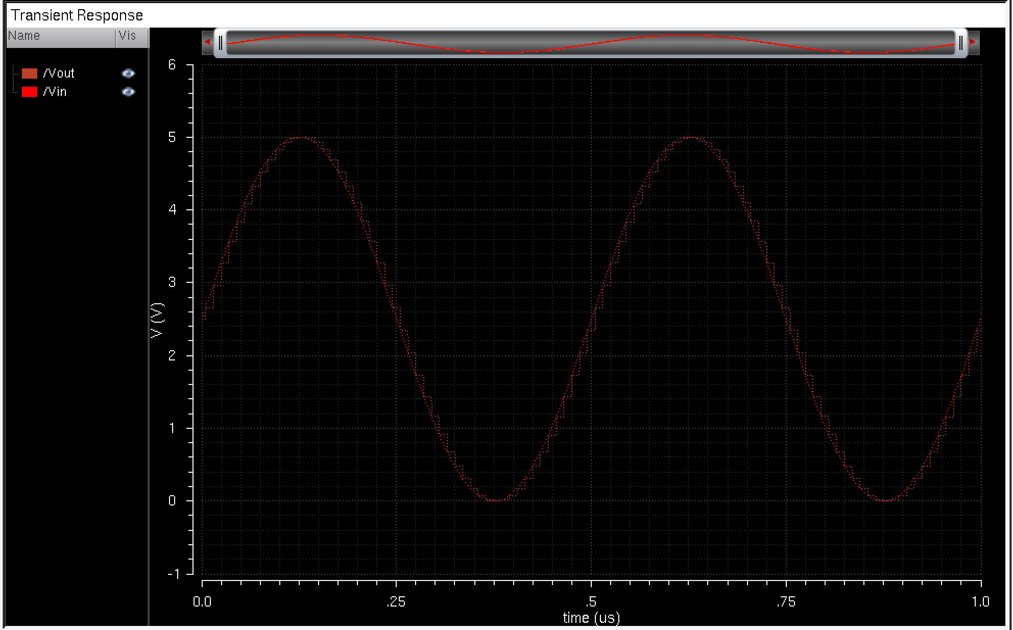
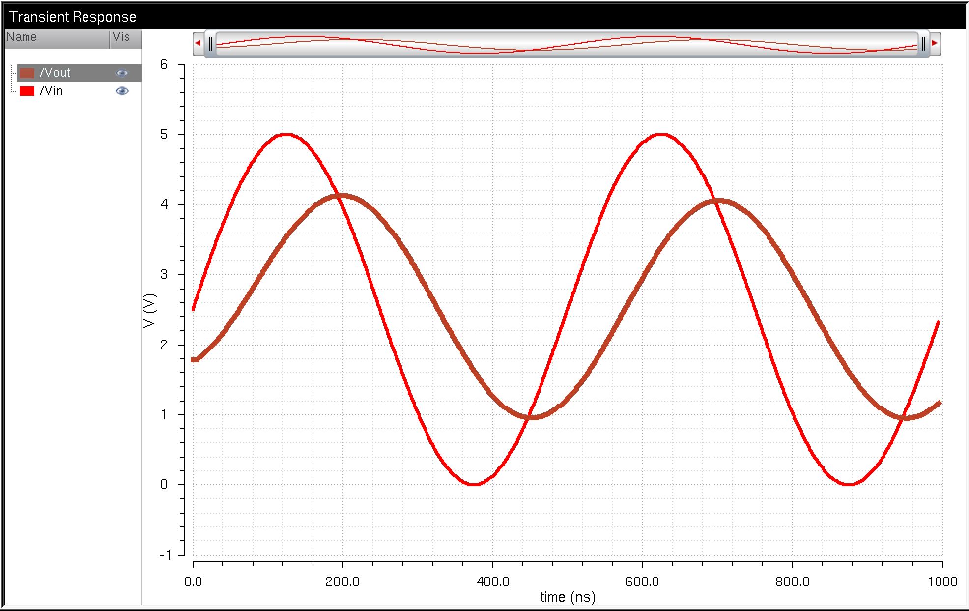
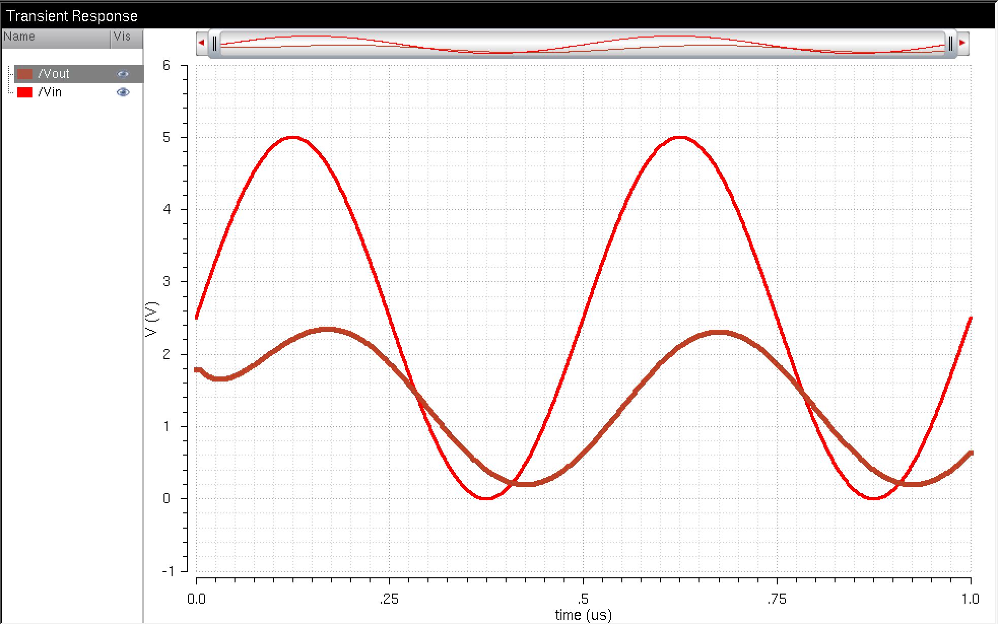
Then we next with a 10pF load and notice a lag of around 70ns
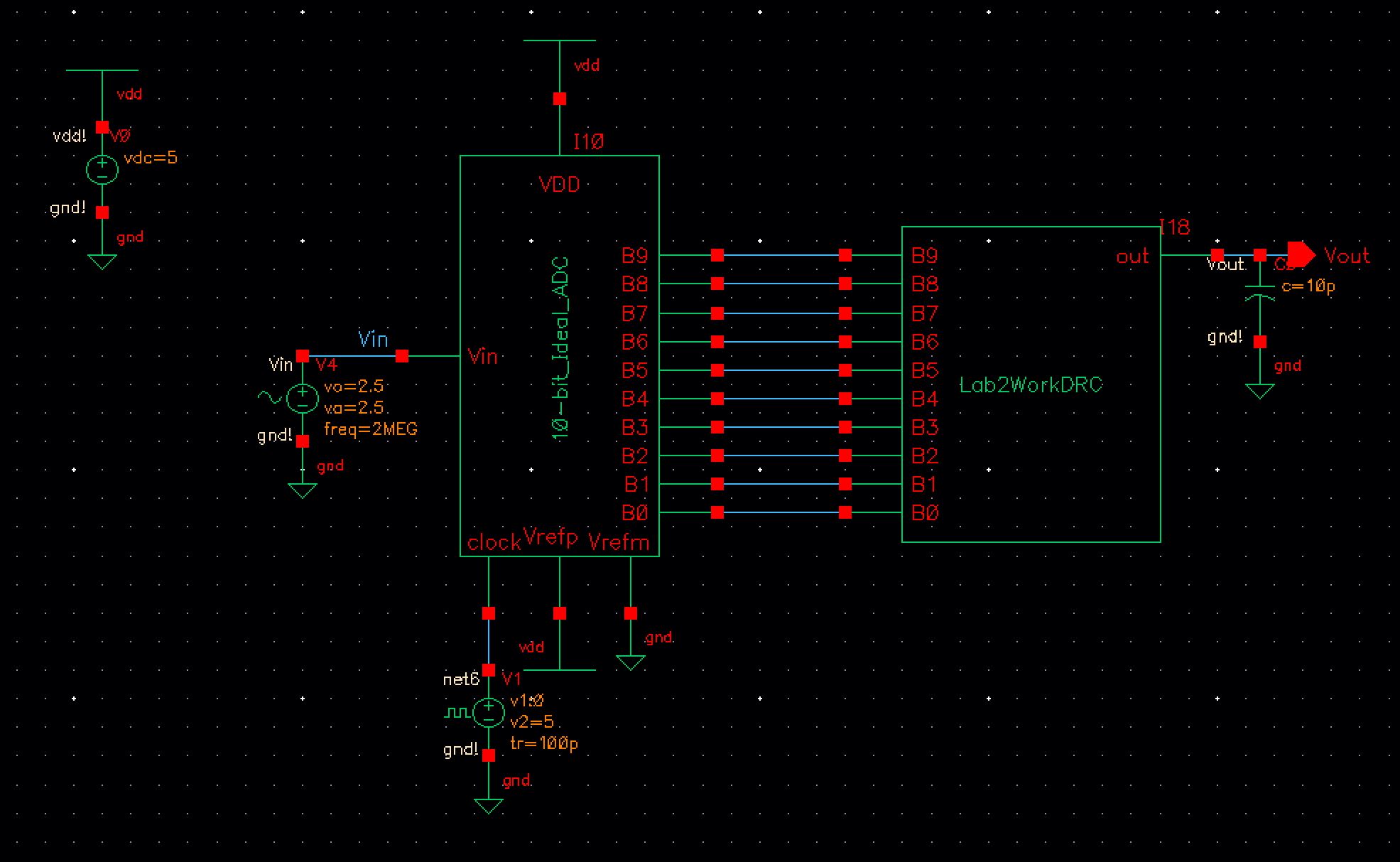
And finally we test by put a in parallel a resistor and capaictor
Conlusion
In
conclusion these simulations showed that the made DAC was woking as
expected. As we saw when there is no load there is a small lag but they
are in phase. When only a resistive load is added to the DAC output is half the input voltage.
When a capacitor is added to the DAC output is smoothed with a delay.
Lastly when we have both a resistive and capacitor are on the load end
the DAC output will experiance a slight lag with a reduced voltage.
Questions
- Explain what happens if the DAC drives a 10k load?
The output becomes half of the input volage because the 10K load makes a volage divider at the output.- In a real circuit the switches seen above (the outputs of the ADC) are implemented with transistors (MOSFETs).
- Discuss what happens if the resistance of the switches isn't small compared to R.
In
a real circuit if the switch resistance was not small compared to R.
Then the equivalent resistace of the DAC would not be R.Recaluating R would have to be done in order to have the right output.
Problems
I had to force the simluation because it would only output half the waveform
Solution
- Set the values as seen below
- relative tolerance, reltol, of 10% (= 1e-1)
- voltage absolute tolerance, vabstol, of 100 mV (= 1e-1)
- current absolute tolerance, iabstol, of 1 mA (= 1e-3)
Backed up work
return to labs