Lab 2 - EE421L
Damian Aceves Franco
acevesfr@unlv.nevada.edu
09/01/2021
Design of a 10-bit digital-to-analog converter (DAC)
Pre-lab work
- Read through this entire lab write-up before doing the pre-lab
- Download lab2.zip to your desktop.
- This
archive contains a simulation example using an ideal 10-bit
Analog-to-Digital Converter (ADC) and Digital-to-Analog Converter
(DAC).
- Prior to coming to lab make sure you understand how the input voltage, Vin, is related to B[9:0] and Vout.
- In your lab report:
- 1) provide narrative of the steps seen above,
- 2) provide, and discuss, simulation results different from the above to illustrate your understanding of the ADC and DAC,
- 3) explain how you determine the least significant bit (LSB, the minumum voltage change on the ADC's input to see a change in the digital code B[9:0]) of the converter. Use simulations to support your understanding.
up load lab2.zip to MobaxTerm and unzip
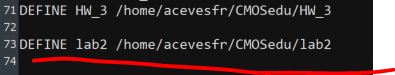
then check to see if the design directory is in the cds.lib if now type it and save
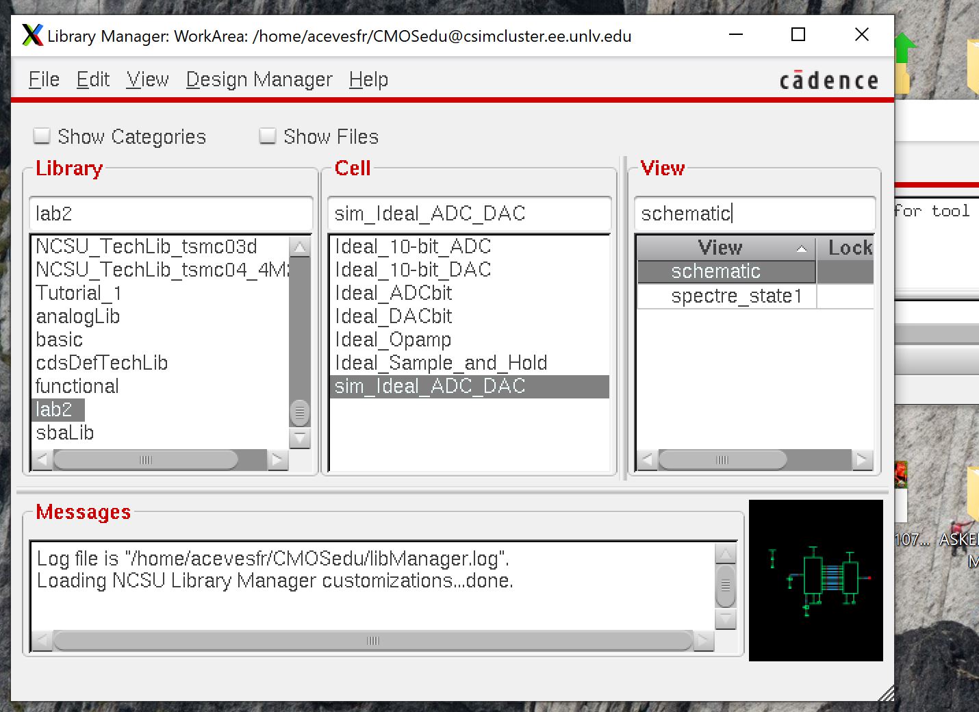
now run virtuoso and open the schematic
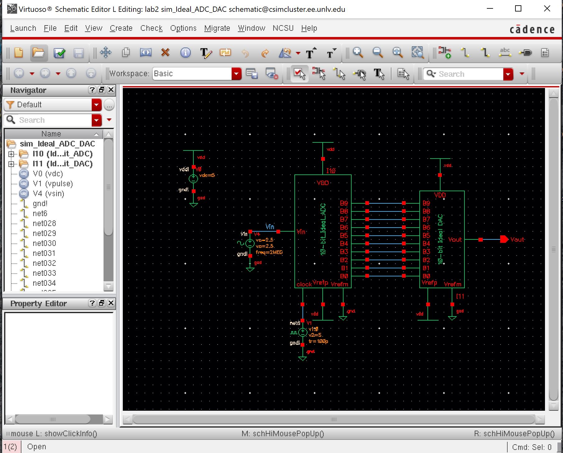
then run ADE L
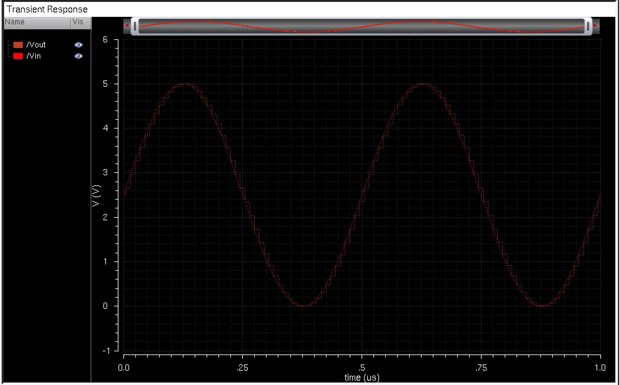
The least significant bit (LSB) is determined my useing the equation 1LSB=(Vdd)/2^n.
in this case the 1LSB is 5/2^10 = 4.88mV
****************************************************************************************************************************************************************************
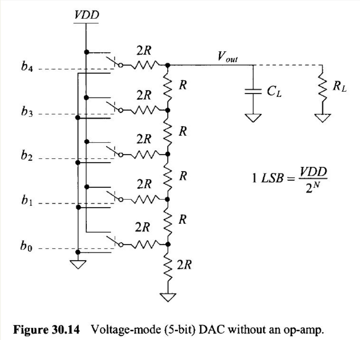
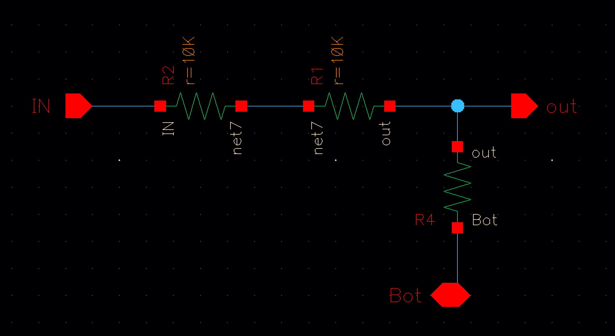
In this lab we'll use n-well resistors to implement a 10-bit DAC.
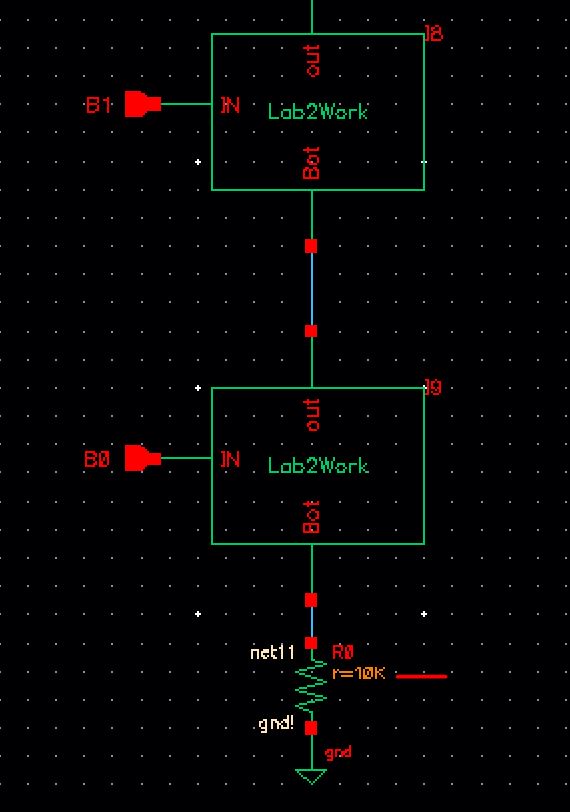
- The design of a 10-bit DAC using an n-well R of 10k
- How to determine the output resistance of the DAC (answer: R) by combining resistors in parallel and series
- Delay, driving a load
- How to create a symbol view for your design with the exact same footprint as the Ideal_10-bit_DAC symbol view
- Simulations to verify your design functions correctly
Our design is based upon the topology seen in Fig. 30.14, below, in the CMOS book.
Desinging 10-Bit DAC using N-well Resistor of 10k
Create a symbol
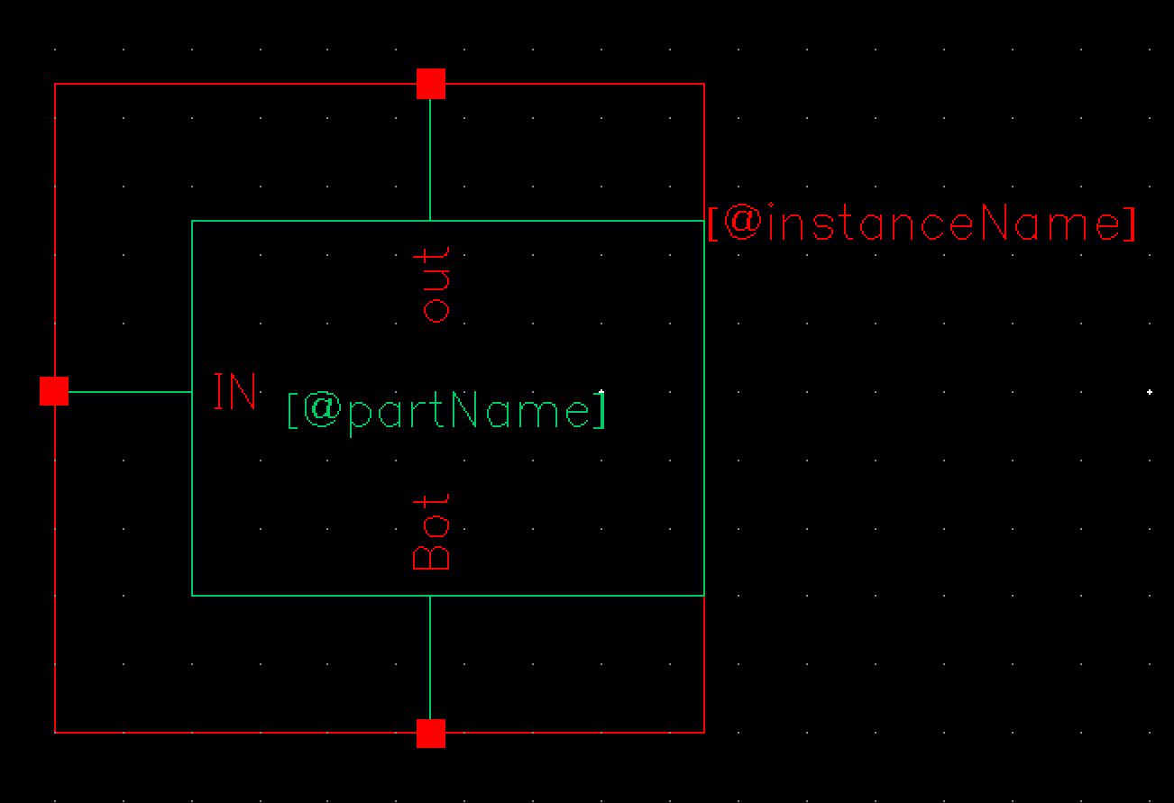
We
are ready to start the fun. Next I created a new schematic and lined up
the new symbol in the following manner to start making the DRC
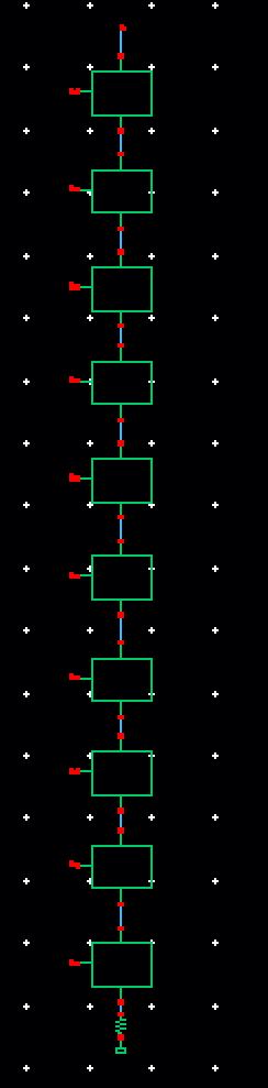
Now we must remember to add a 10K resisitor at the bottom in between the symbol and gound
return to labs